

Page 1
Abstract
This technical data sheet describes the stand-alone NINA-B3 series Bluetooth® 5 low energy
modules. The NINA-B3 series includes two variants - NINA-B30 and NINA-B31 series. The NINA-B30
series provides an open CPU architecture with a powerful MCU for customer applications, while the
NINA-B31 series are delivered with u-blox connectivity software pre-flashed.
www.u-blox.com
UBX-17052099 - R02
🆂
NINA-B3 series
Stand-alone Bluetooth 5 low energy modules
Data Sheet
Page 2

NINA-B3 series - Data Sheet
Title
NINA-B3 series
Subtitle
Stand-alone Bluetooth 5 low energy modules
Document type
Data Sheet
Document number
UBX-17052099
Revision and date
R02
10-Sep-2018
Disclosure Restriction
Product status
Corresponding content status
Functional Sample
Draft
For functional testing. Revised and supplementary data will be published later.
In Development /
Prototype
Objective Specification
Target values. Revised and supplementary data will be published later.
Engineering Sample
Advance Information
Data based on early testing. Revised and supplementary data will be published later.
Initial Production
Early Production Information
Data from product verification. Revised and supplementary data may be published later.
Mass Production /
End of Life
Production Information
Document contains the final product specification.
Product name
Type number
u-blox connectivity software
version
PCN reference
Product status
NINA-B311
NINA-B311-00B-00
1.0.0
N/A
Engineering Sample
NINA-B312
NINA-B312-00B-00
1.0.0
N/A
NINA-B301
NINA-B301-00B-00
-
N/A
NINA-B302
NINA-B302-00B-00
-
N/A
u-blox or third parties may hold intellectual property rights in the products, names, logos and designs included in this
document. Copying, reproduction, modification or disclosure to third parties of this document or any part thereof is only
permitted with the express written permission of u-blox.
The information contained herein is provided “as is” and u-blox assumes no liability for its use. No warranty, either express or
implied, is given, including but not limited to, with respect to the accuracy, correctness, reliability and fitness for a particular
purpose of the information. This document may be revised by u-blox at any time without notice. For the most recent
documents, visit www.u-blox.com.
Copyright © u-blox AG.
Document Information
This document applies to the following products:
UBX-17052099 - R02 Page 2 of 50
Page 3

NINA-B3 series - Data Sheet
Contents
Document Information ................................................................................................................................ 2
Contents .......................................................................................................................................................... 3
1 Functional description ......................................................................................................................... 6
1.1 Overview ........................................................................................................................................................ 6
1.2 Applications ................................................................................................................................................. 6
1.3 Product features ......................................................................................................................................... 7
1.3.1 NINA-B30 series .................................................................................................................................. 7
1.3.2 NINA-B31 series ................................................................................................................................... 7
1.4 Block diagram .............................................................................................................................................. 8
1.4.1 NINA-B311 ............................................................................................................................................. 8
1.4.2 NINA-B312 ............................................................................................................................................ 8
1.5 Product description .................................................................................................................................... 9
1.6 Hardware options ........................................................................................................................................ 9
1.7 Software options ......................................................................................................................................... 9
1.7.1 u-blox connectivity software .......................................................................................................... 10
1.7.2 Open CPU............................................................................................................................................ 10
1.8 Bluetooth device address ........................................................................................................................ 10
2 Interfaces ............................................................................................................................................... 12
2.1 Power management ..................................................................................................................................12
2.1.1 Module supply input (VCC) ..............................................................................................................12
2.1.2 Digital I/O interfaces reference voltage (VCC_IO) .......................................................................12
2.2 RF antenna interfaces ..............................................................................................................................12
2.2.1 2.4 GHz Bluetooth low energy (ANT) ..............................................................................................12
2.2.2 Near Field Communication (NFC) ...................................................................................................12
2.3 System functions ...................................................................................................................................... 13
2.3.1 Module power-on .............................................................................................................................. 13
2.3.2 Module power off .............................................................................................................................. 13
2.3.3 Standby mode ................................................................................................................................... 13
2.3.4 Sleep mode ......................................................................................................................................... 14
2.3.5 Module reset ...................................................................................................................................... 14
2.3.6 CPU and memory .............................................................................................................................. 14
2.3.7 Direct Memory Access ..................................................................................................................... 14
2.3.8 Programmable Peripheral Interconnect ....................................................................................... 14
2.3.9 Real Time Counter (RTC) ................................................................................................................. 15
2.4 Serial interfaces ........................................................................................................................................ 15
2.4.1 Universal Asynchronous Receiver/Transmitter (UART) ........................................................... 15
2.4.2 Serial peripheral interface (SPI) ..................................................................................................... 16
2.4.3 Quad serial peripheral interface (QSPI) ........................................................................................ 16
2.4.4 I2C interface ....................................................................................................................................... 16
2.4.5 I2S interface......................................................................................................................................... 17
UBX-17052099 - R02 Page 3 of 50
Page 4

NINA-B3 series - Data Sheet
2.4.6 USB 2.0 interface ............................................................................................................................... 17
2.5 Digital interfaces ........................................................................................................................................ 17
2.5.1 PWM ..................................................................................................................................................... 17
2.5.2 PDM ...................................................................................................................................................... 17
2.5.3 QDEC ................................................................................................................................................... 18
2.6 Analog interfaces ...................................................................................................................................... 18
2.6.1 ADC ...................................................................................................................................................... 18
2.6.2 Comparator ........................................................................................................................................ 18
2.6.3 Low power comparator .................................................................................................................... 19
2.6.4 Analog pin options ............................................................................................................................ 19
2.7 GPIO ............................................................................................................................................................. 19
2.8 u-blox connectivity software features .................................................................................................. 20
2.8.1 u-blox Serial Port Service (SPS) ..................................................................................................... 20
2.8.2 System status signals ..................................................................................................................... 20
2.8.3 System control signals .................................................................................................................... 20
2.8.4 UART signals ......................................................................................................................................21
2.9 Debug interfaces ........................................................................................................................................21
2.9.1 SWD ......................................................................................................................................................21
2.9.2 Trace – Serial Wire Output ...............................................................................................................21
2.9.3 Parallel Trace ......................................................................................................................................21
3 Pin definition ......................................................................................................................................... 22
3.1 NINA-B30 series pin assignment ........................................................................................................... 22
3.2 NINA-B31 series pin assignment (with u-blox connectivity software) ........................................... 25
4 Electrical specifications ................................................................................................................... 28
4.1 Absolute maximum ratings .................................................................................................................... 28
4.1.1 Maximum ESD ratings ..................................................................................................................... 28
4.2 Operating conditions ................................................................................................................................ 28
4.2.1 Operating temperature range ........................................................................................................ 28
4.2.2 Supply/Power pins ............................................................................................................................ 29
4.2.3 Current consumption ....................................................................................................................... 29
4.2.4 RF performance ................................................................................................................................30
4.2.5 RESET_N pin ......................................................................................................................................30
4.2.6 Digital pins ..........................................................................................................................................30
4.2.7 I2C pull-up resistor values................................................................................................................30
4.2.8 Analog comparator ........................................................................................................................... 31
5 Mechanical specifications ............................................................................................................... 32
5.1 NINA-B3x1 Mechanical specification .................................................................................................... 32
5.2 NINA-B3X2 Mechanical specifications ................................................................................................. 34
6 Qualification and approvals............................................................................................................. 36
6.1 Country approvals ..................................................................................................................................... 36
6.2 FCC/IC Compliance ................................................................................................................................... 36
6.2.1 Open CPU responsibility and obligations ..................................................................................... 36
UBX-17052099 - R02 Page 4 of 50
Page 5

NINA-B3 series - Data Sheet
6.2.2 RF-exposure statement .................................................................................................................. 37
6.2.3 End-product user manual instructions ........................................................................................ 38
6.2.4 End-product labeling requirements .............................................................................................. 38
6.2.5 End-product compliance ................................................................................................................. 39
6.3 Safety Compliance .................................................................................................................................... 40
6.4 Bluetooth qualification information ...................................................................................................... 40
7 Antennas ................................................................................................................................................ 41
7.1 Antenna accessories ................................................................................................................................ 41
7.1.1 Single band antennas ...................................................................................................................... 41
8 Product handling ................................................................................................................................. 45
8.1 Packaging ................................................................................................................................................... 45
8.1.1 Reels .................................................................................................................................................... 45
8.1.2 Tapes ................................................................................................................................................... 45
8.2 Moisture sensitivity levels ....................................................................................................................... 45
8.3 Reflow soldering ........................................................................................................................................ 45
8.4 ESD precautions ........................................................................................................................................ 45
9 Labeling and ordering information ............................................................................................... 46
9.1 Product labeling ......................................................................................................................................... 46
9.2 Explanation of codes ................................................................................................................................ 46
9.3 Ordering information ................................................................................................................................ 47
Appendix ....................................................................................................................................................... 48
A Glossary ................................................................................................................................................. 48
Related documents ................................................................................................................................... 49
Revision history .......................................................................................................................................... 49
Contact .......................................................................................................................................................... 50
UBX-17052099 - R02 Page 5 of 50
Page 6

NINA-B3 series - Data Sheet
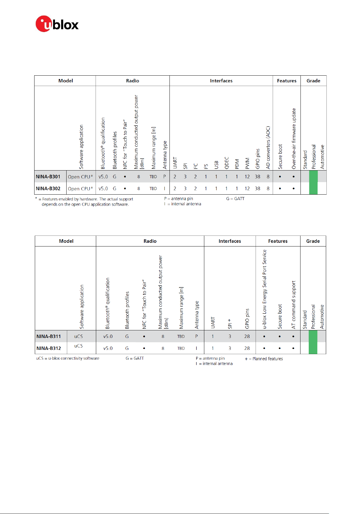
Model
Description
NINA-B30 series
Bluetooth 5 module with a powerful Arm Cortex-M4 with FPU, and state-of-the-art power performance.
Both the variants of NINA-B30 are open CPU modules that enable customer applications to run on the
built-in Arm Cortex-M4 with FPU. With 1 MB flash and 256 kB RAM, they offer the best-in-class capacity
for customer applications on top of the Bluetooth low energy stack. NINA-B302 comes with an internal
antenna, while NINA-B301 has a pin for use with an external antenna. The internal PIFA antenna is
specifically designed for the small NINA form factor and provides an extensive range, independent of
ground plane and component placement.
NINA-B31 series
Bluetooth 5 module with a powerful Arm Cortex-M4 with FPU and u-blox connectivity software preflashed. The connectivity software in NINA-B31 modules provides support for u-blox Bluetooth low energy
Serial Port Service, GATT client and server, beacons, NFC™, and simultaneous peripheral and central roles
– all configurable from a host using AT commands. The NINA-B31x modules provide top grade security,
thanks to secure boot, which ensures the module only boots up with original u-blox software. NINA-B312
comes with an internal antenna, while NINA-B311 has a pin for use with an external antenna. The internal
PIFA antenna is specifically designed for the small NINA form factor and provides an extensive range,
independent of ground plane and component placement.
1 Functional description
1.1 Overview
The NINA-B3 series modules are small stand-alone Bluetooth 5 low energy modules featuring full
Bluetooth 5 support, a powerful Arm® Cortex®-M4 with FPU, and state-of-the-art power
performance. The embedded low power crystal improves power consumption by enabling optimal
power save modes.
The NINA-B3 series includes the following two variants as listed in the table below:
The NINA-B3 series modules are globally certified for use with the internal antenna or a range of
external antennas. This greatly reduces time, cost, and effort for customers integrating these
modules in their designs.
1.2 Applications
Industrial automation
Smart buildings and cities
Low power sensors
Wireless-connected and configurable equipment
Point-of-sales
Health devices
UBX-17052099 - R02 Functional description Page 6 of 50
Page 7
NINA-B3 series - Data Sheet
1.3 Product features
1.3.1 NINA-B30 series
Table 1: NINA-B30 series main features summary
1.3.2 NINA-B31 series
Table 2: NINA-B31 series main features summary
UBX-17052099 - R02 Functional description Page 7 of 50
Page 8
NINA-B3 series - Data Sheet
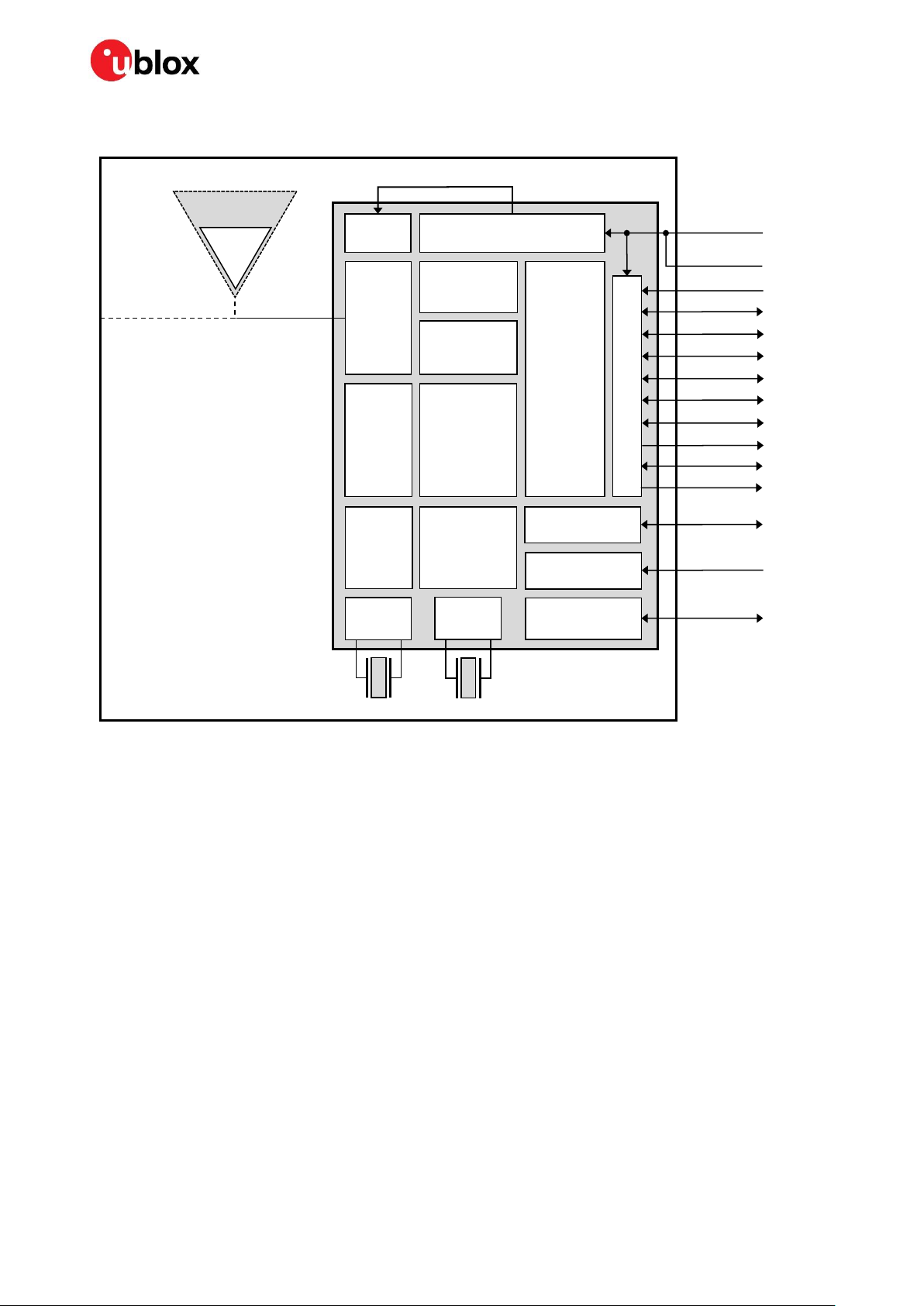
DC/DC and LDO regulators
BLE baseband
Cryptographic
accelerators
IO Buffers
PLL
VCC_IO (1.7 – 3.6 V)
VCC (1.7 - 3.6 V)
32 MHz
Reset
UART
SPI
GPIO
1.3 V
power
I2C
PWM
I2S
comparator
Analog
NFC
32.768 kHz
RTC, Timers
Antenna pin
NINA-B3x1
Nordic Semiconductor
nRF52840
QSPI
USB 2.0
QDEC
PDM
CryptoCell
1.4 Block diagram
PIFA antenna
(NINA-B3x2)
System
hardware
RF
256 kB
RAM
1 MB Flash
and Counters
PLL
Arm Cortex-M4
USB device
ADC and
Passive NFC tag
Figure 1: Block diagram of NINA-B3 series
1.4.1 NINA-B311
The NINA-B311 modules do not use the internal antenna and thus the PCB has been trimmed to
allow for a smaller module (10.0 x 11.6 mm). Instead of an internal antenna, the RF signal is available
at a module pin for routing to an external antenna or antenna connector.
1.4.2 NINA-B312
The NINA-B312 modules use an internal metal sheet PIFA antenna mounted on the PCB (10.0 x 15.0
mm). The RF signal pin is not connected to any signal path.
UBX-17052099 - R02 Functional description Page 8 of 50
Page 9

NINA-B3 series - Data Sheet
Item
NINA-B3x1
NINA-B3x2
Bluetooth version
5.0
5.0
Band support
2.4 GHz, 40 channels
2.4 GHz, 40 channels
Typical conducted output power
+7.5 dBm
+8 dBm
Radiated output power (EIRP)
+10.5 dBm (with approved antennas)
+10 dBm
RX sensitivity (conducted)
-94 dBm
-94 dBm
RX sensitivity, long range mode
(conducted)
-100 dBm
-100 dBm
Supported BLE data rates
1 Mbps
2 Mbps
500 kbps
125 kbps
1 Mbps
2 Mbps
500 kbps
125 kbps
Module size
10.0 x 11.6 mm
10.0 x 15.0 mm
1.5 Product description
Table 3: NINA-B3 series characteristics summary
1.6 Hardware options
Except for the different PCB sizes and antenna solutions, the NINA-B3 series modules use an
identical hardware configuration. An on-board 32.768 KHz crystal is included as well as an integrated
DC/DC converter for higher efficiency under heavy load situations (see section 2.1.1 for more
information).
1.7 Software options
The integrated application processor of the NINA-B3 module is an Arm Cortex-M4 with FPU that has
1 MB flash memory and 256 kB RAM. The NINA-B3 modules support additional external memory that
can be connected to the Quad Serial Peripheral Interface (QSPI); see section 2.4.3 for additional
information. The software structure of any program running on the module can be broken down into
the following components:
Radio stack
Bootloader (optional)
Application
UBX-17052099 - R02 Functional description Page 9 of 50
Page 10
NINA-B3 series - Data Sheet
Figure 2: NINA-B3 software structure and available software options
NINA-B3 Software
structure
Radio
Stack
Applicatio
NINA-B31 series
Nordic S140 SoftDevice
u-blox
Nordic
SDK
Wirepas mesh
NINA-B30 series options
Bootloader
Connectivity
connectivity
software
Software
+
SDK
1.7.1 u-blox connectivity software
The NINA-B31 series modules are pre-flashed with u-blox connectivity software.
The u-blox connectivity software enables use of the u-blox Low Energy Serial Port Service, controlled
by AT commands over the UART interface. The NINA-B31 modules can be configured using the ublox s-center evaluation software, which can be downloaded from the u-blox website and is available
free of charge.
Much more information on the features and capabilities of the u-blox connectivity software and how
to use it can be found in the
u-blox Short Range AT Commands Manual [2]
.
1.7.2 Open CPU
The open CPU architecture in the NINA-B30 series modules allows you to build your own
applications. u-blox recommends the following development approaches to speed up the process:
1.7.2.1 Nordic SDK
The Nordic Semiconductors nRF5 SDK provides a rich and well-tested software development
environment for nRF52 based devices. It includes a broad selection of drivers, libraries, and example
applications. It also includes other radio stacks.
The NINA-B3 series modules are only certified for use with the S140 Bluetooth Low Energy
SoftDevice. If you would like to use another 2.4 GHz radio protocol, contact u-blox support for your
area as listed in the Contact section.
1.7.2.2 Wirepas connectivity software
The NINA-B30 series modules can also be used together with the Wirepas software stack. This will
enable the NINA-B30 module to be used in a large scale mesh environment.
The Wirepas connectivity software is a third party licensed software from Wirepas.
For more information about the Wirepas connectivity software, contact the u-blox support for your
area as listed in the Contact section or contact Wirepas directly.
1.8 Bluetooth device address
UBX-17052099 - R02 Functional description Page 10 of 50
Page 11

NINA-B3 series - Data Sheet
Each NINA-B31 module is pre-programmed with a unique 48-bit Bluetooth device address. For
NINA-B30 series modules, or if the memory of a NINA-B31 module is corrupted or otherwise lost, the
address can be recovered from the data matrix barcode printed on the module label.
UBX-17052099 - R02 Functional description Page 11 of 50
Page 12

NINA-B3 series - Data Sheet
2 Interfaces
2.1 Power management
2.1.1 Module supply input (VCC)
The NINA-B3 series uses integrated step-down converters to transform the supply voltage
presented at the VCC pin into a stable system voltage. Because of this, the NINA-B3 modules are
compatible for use in battery powered designs without the use of an additional voltage converter.
You can choose one of the following two on-board voltage converter options:
A low-dropout (LDO) converter
A DC/DC buck converter
Normally, the module will automatically switch between these options depending on the current
consumption of the module. Under high loads such as when the radio is active, the DC/DC converter
is more efficient, while the LDO converter is more efficient in the power saving modes.
2.1.2 Digital I/O interfaces reference voltage (VCC_IO)
All modules in the u-blox NINA series provide an additional voltage supply input for setting the I/O
voltage level. In NINA-B3 series modules, the I/O voltage level is similar to the supply voltage and
VCC_IO is internally connected to the supply input. Therefore, only a single supply voltage is needed
for NINA-B3, which makes it ideal for battery powered designs.
☞ This may not be the case for other modules in the NINA series. A design that should be pin
compatible with other NINA-series modules should keep the VCC and VCC_IO supply rails
separate.
2.2 RF antenna interfaces
2.2.1 2.4 GHz Bluetooth low energy (ANT)
The three NINA-B3 model versions have their own 2.4 GHz antenna solutions respectively:
The NINA-B311 modules provide an antenna pin (ANT) with a nominal characteristic impedance
of
50 Ω. This pin can be connected to an onboard antenna or antenna connector using a controlled
impedance trace.
The NINA-B312 modules use an integrated antenna solution; no additional components are
required. The antenna is a metal sheet PIFA antenna that makes the module insensitive to
placement on the carrier board or the size of the carrier board, when compared to other
integrated antenna solutions. The ANT pin is internally disconnected on these models.
2.2.2 Near Field Communication (NFC)
The NINA-B3 series modules include a Near Field Communication interface, capable of operating as
a 13.56 MHz NFC tag at a bit rate of 106 kbps. As an NFC tag, the data can be read from or written to
the NINA-B3 modules using an NFC reader; however, the NINA-B3 modules are not capable of
reading other tags or initiating NFC communications. The NFC interface can be used to wake the
module from sleep mode, meaning that the module can be kept in the deepest power save mode and
wake up and properly react to an NFC field.
Two pins are available for connecting to an external NFC antenna: NFC1 and NFC2.
UBX-17052099 - R02 Interfaces Page 12 of 50
Page 13

NINA-B3 series - Data Sheet
2.3 System functions
The NINA-B3 series modules are power efficient devices capable of operating in different power
saving modes and configurations. Different sections of the module can be powered off when not
needed and complex wake- up events can be generated from different external and internal inputs.
The radio part of the module operates independently from the CPU. The three main power modes
are:
Active
Standby
Sleep
Depending on the application, the module should spend most of its time in either standby or sleep
mode to minimize current consumption.
2.3.1 Module power-on
You can switch on or reboot the NINA-B3 modules in one of the following ways:
Rising edge on the VCC pin to a valid supply voltage
Issuing a reset of the module (see section 2.3.5)
An event to wake up from the sleep mode to the active mode can be triggered by:
A programmable digital or analog sensor event. For example, rising voltage level on an analog
comparator pin
Detecting an NFC field
Supplying 5 V to the VBUS pin (plugging in the USB interface)
While waking up from the standby mode to active mode, an event can also be triggered by:
The on-board Real Time Counter (RTC)
The radio interface
2.3.2 Module power off
There is no dedicated pin to power off the NINA-B3 modules. You can configure any GPIO pin to enter
or exit the sleep mode (see section 2.3.4), which essentially powers down the module.
An under-voltage (brown-out) shutdown occurs on the NINA-B3 modules when the VCC supply
drops below the operating range minimum limit. If this occurs, it is not possible to store the current
parameter settings in the module’s non-volatile memory. An over temperature and under
temperature shutdown can be enabled on the NINA-B3 modules, and is initiated if the temperature
measured within the module is outside operating conditions. The temperature is measured by an
integrated temperature sensor in the radio chip.
2.3.3 Standby mode
Standby mode is one of the power saving modes in NINA-B3 modules that essentially powers down
the module but keeps the system RAM and configurations intact. It also allows for complex,
autonomous power-up events including periodic RTC events and radio events.
The following events can be used to bring the module out of the standby mode:
Internal wake-up events from the RTC, radio, NFC and so on.
Analog or digital sensor events (programmable voltage level or edge detection)
During standby mode, the module is clocked at 32 kHz, which is generated by an internal 32 kHz
crystal oscillator.
UBX-17052099 - R02 Interfaces Page 13 of 50
Page 14

NINA-B3 series - Data Sheet
2.3.4 Sleep mode
Sleep mode is the deepest power saving mode of NINA-B3 modules. During sleep mode, all
functionality is stopped to ensure minimum power consumption. The module needs an external
event in order to wake up from the sleep mode. The module will always reboot after waking up from
the sleep mode; however different sections of the RAM can be configured to remain intact during
and after going to the sleep mode.
The following events can be used to wake up the module out of the sleep mode:
External event on a digital pin
External analog event on a low power comparator pin
Detection of an NFC field
When using the u-blox connectivity software, the module can be manually switched on or off with
proper storage of the current settings using the UART DSR pin.
The module can be programmed to latch the digital values present at its GPIO pins during sleep. The
module will keep the values latched, and a change of state on any of these pins will trigger a wake-up
to active mode.
2.3.5 Module reset
You can reset the NINA-B3 modules using one of the following ways:
Low level on the RESET_N input pin, normally kept high using an internal pull-up. This causes an
“external” or “hardware” reset of the module. The current parameter settings are not saved in
the module’s non-volatile memory and a proper network detach is not performed.
Using the AT+CPWROFF command. This causes an “internal” or “software” reset of the module.
The current parameter settings are saved in the module’s non-volatile memory and a proper
network detach is performed.
2.3.6 CPU and memory
The Nordic Semiconductor nRF52840 chip in the NINA-B3 series modules includes a powerful Arm
Cortex M4 processor. The processor works with a superset of 16 and 32-bit instructions (Thumb-2)
at 64 MHz clock speed. It can use up to 37 interrupt vectors and 3 priority bits.
The nRF52840 chip has 1 MB of flash and 256 KB of RAM for code and data storage. Additionally, up
to 4 GB of external memory can be addressed with Execute in Place (XIP) support via the QSPI
interface. See Section 2.4.3 for additional information.
2.3.7 Direct Memory Access
All interfaces described in this data sheet support Direct Memory Access (DMA) to move any data
generated from the interface directly into the RAM, without involving the CPU. This ensures fluent
operation of the CPU with minimal need for interruption. To reduce the overall power consumption,
DMA should be used as often as possible.
2.3.8 Programmable Peripheral Interconnect
The Nordic Semiconductor nRF52840 chip in the NINA-B3 series modules include a programmable
peripheral interconnect (PPI), which is basically a switch matrix that connects various control signals
between different interfaces and system functions. This allows most interfaces to bypass the CPU
in order to trigger a system function, that is, an incoming data packet may trigger a counter or a
falling voltage level on an ADC, might toggle a GPIO, all without having to send an interrupt to the
CPU. This enables smart applications that are extremely power efficient that wake up the CPU only
when it is needed.
UBX-17052099 - R02 Interfaces Page 14 of 50
Page 15

NINA-B3 series - Data Sheet
2.3.9 Real Time Counter (RTC)
A key system feature available on the module is the Real Time Counter. This counter can generate
multiple interrupts and events to the CPU and radio as well as internal and external hardware blocks.
These events can be precisely timed ranging from microseconds up to hours, and allows for periodic
BLE advertising events etc., without involving the CPU. The RTC can be operated in the active and
standby modes.
2.4 Serial interfaces
NINA-B3 modules provide the following serial communication interfaces:
2x UART interfaces: 4-wire universal asynchronous receiver/transmitter interface used for AT
command interface, data communication, and u-blox connectivity software upgrades using the
Software update+UFWUPD AT command.
3x SPI interfaces: Up to three serial peripheral interfaces can be used simultaneously.
1x QSPI interface: High speed interface used to connect to the external flash memories.
2x I2C interfaces: Inter-Integrated Circuit (I2C) interface for communication with digital sensors.
1x I2S interface: Used to communicate with external audio devices.
1x USB 2.0 interface: The USB device interface to connect to the upstream host.
☞ Most digital interface pins on the module are shared between the digital, analog interfaces and
GPIOs. Unless otherwise stated, all functions can be assigned to any pin that is not already
occupied.
☞ Two of the SPI interfaces share common hardware with the I
used simultaneously. That is, if both the I2C interfaces are in use then only one SPI interface will
be available.
2.4.1 Universal Asynchronous Receiver/Transmitter (UART)
The 4-wire UART interface supports hardware flow control and baud rates up to 1 Mbps. Other
characteristics of the UART interface are listed below:
Pin configuration:
o TXD, data output pin
o RXD, data input pin
o RTS, Request To Send, flow control output pin (optional)
o CTS, Clear To Send, flow control input pin (optional)
Hardware flow control or no flow control (default) is supported.
Power saving indication available on the hardware flow control output (RTS pin): The line is driven
to the OFF state when the module is not ready to accept data signals.
Programmable baud rate generator allows most industry standard rates, as well as non-
standard rates up to 1 Mbps.
Frame format configuration:
o 8 data bits
o Even or no-parity bit
o 1 stop bit
Default frame configuration is 8N1, meaning eight (8) data bits, no (N) parity bit, and one (1) stop
bit.
Frames are transmitted in such a way that the least significant bit (LSB) is transmitted first.
2
C interfaces and they cannot be
UBX-17052099 - R02 Interfaces Page 15 of 50
Page 16

NINA-B3 series - Data Sheet
2.4.2 Serial peripheral interface (SPI)
NINA-B3 supports up to three Serial Peripheral Interfaces with serial clock frequencies of up to 8
MHz. Characteristics of the SPI interfaces are listed below:
Pin configuration in master mode:
o SCLK, Serial clock output, up to 8 MHz
o MOSI, Master Output Slave Input data line
o MISO, Master Input Slave Output data line
o CS, Chip/Slave select output, active low, selects which slave on the bus to talk to.
Only one select line is enabled by default but more can be added by customizing a
GPIO pin.
o DCX, Data/Command signal, this signal is optional but is sometimes used by the SPI
slaves to distinguish between SPI commands and data
Pin configuration in slave mode:
o SCLK, Serial clock input
o MOSI, Master Output Slave Input data line
o MISO, Master Input Slave Output data line
o CS, Chip/Slave select input, active low, connects/disconnects the slave interface from
the bus.
Both master and slave modes are supported on all the interfaces.
The serial clock supports both normal and inverted clock polarity (CPOL) and data should be
captured on rising or falling clock edge (CPHA).
2.4.3 Quad serial peripheral interface (QSPI)
The Quad Serial Peripheral Interface enables external memory to be connected to the NINA-B3
module to increase the application program size. The QSPI supports Execute In Place (XIP), which
allows CPU instructions to be read and executed directly from the external memory (128 MB at a
time with a programmable offset). Characteristics for the QSPI are listed below:
The QSPI always operates in master mode and uses the following pin configuration:
o CLK, serial clock output, up to 32 MHz
o CS, Chip/Slave select output, active low, selects which slave on the bus to talk to
o D0, MOSI serial output data in single mode, data I/O signal in dual/quad mode
o D1, MISO serial input data in single mode, data I/O signal in dual/quad mode
o D2, data I/O signal in quad mode (optional)
o D3, data I/O signal in quad mode (optional)
Single/dual/quad read and write operations (1/2/4 data signals)
Clock speeds between 2 – 32 MHz
Data rates up to 128 Mbit/s in the quad mode
32 bit addressing can address up to 4 GB of data
Instruction set includes support for deep power down mode of the external flash
Possible to generate custom flash instructions containing a 1 byte opcode and up to 8 bytes of
additional data and read its response
2.4.4 I
2
C interface
The Inter-Integrated Circuit interfaces can be used to transfer and/or receive data on a 2-wire bus
network. The NINA-B3 modules can operate as both master and slave on the I2C bus using standard
(100 kbps), fast (400 kbps), and 250 kbps transmission speeds. The interface supports clock
stretching, thus allowing NINA-B3 to temporarily pause any I2C communications. Up to 127
individually addressable I2C devices can be connected to the same two signals.
Pin configuration:
o SCL, clock output in master mode, input in slave mode
UBX-17052099 - R02 Interfaces Page 16 of 50
Page 17

NINA-B3 series - Data Sheet
o SDL, data input/output pin
This interface requires external pull-up resistors to work properly in the master mode; see section
4.2.7 for suggested resistor values. The pull-up resistors are required in the slave mode as well but
should be placed at the master end of the interface.
2.4.5 I
The Inter-IC Sound (I2S) interface can be used to transfer audio sample streams between NINA-B3
and external audio devices such as codecs, DACs, and ADCs. It supports original I2S and left or rightaligned interface formats in both master and slave modes.
Pin configuration:
The Master side of an I2S interface always provides the LRCK and SCK clock signals, but some
master devices cannot generate a MCK clock signal. NINA-B3 can supply a MCK clock signal in both
master and slave modes to provide to those external systems that cannot generate their own clock
signal. The two data signals - SDIN and SDOUT allow for simultaneous bi-directional audio
streaming. The interface supports 8, 16, and 24-bit sample widths with up to 48 kHz sample rate.
2
S interface
o MCK, Master clock
o LRCK, Left Right/Word/Sample clock
o SCK, Serial clock
o SDIN, Serial data in
o SDOUT, Serial data out
2.4.6 USB 2.0 interface
The NINA-B3 series modules include a full speed Universal Serial Bus (USB) device interface which is
compliant to version 2.0 of the USB specification. Characteristics of the USB interface include:
Full speed device, up to 12 Mbit/s transfer speed
MAC and PHY implemented in the hardware
Pin configuration:
o VBUS, 5 V supply input, required to use the interface
o USB_DP, USB_DM, differential data pair
Automatic or software controlled pull-up of the USB_DP pin
The USB interface has a dedicated power supply that requires a 5 V supply voltage to be applied to
the VBUS pin. This allows the USB interface to be used even though the rest of the module might be
battery powered or supplied by a 1.8 V supply etc.
2.5 Digital interfaces
2.5.1 PWM
The NINA-B3 modules provide up to 12 independent PWM channels that can be used to generate
complex waveforms. These waveforms can be used to control motors, dim LEDs, or as audio signals
if connected to the speakers. Duty-cycle sequences may be stored in the RAM to be chained and
looped into complex sequences without CPU intervention. Each channel uses a single GPIO pin as
output.
2.5.2 PDM
The pulse density modulation interface is used to read signals from external audio frontends like
digital microphones. It supports single or dual-channel (left and right) data input over a single GPIO
pin. It supports up to 16 kHz sample rate and 16 bit samples. The interface uses the DMA to
automatically move the sample data into RAM without CPU intervention. The interface uses two
signals - CLK to output the sample clock and DIN to read the sample data.
UBX-17052099 - R02 Interfaces Page 17 of 50
Page 18

NINA-B3 series - Data Sheet
2.5.3 QDEC
The quadrature decoder is used to read quadrature encoded data from mechanical and optical
sensors in the form of digital waveforms. Quadrature encoded data is often used to indicate rotation
of a mechanical shaft in either a positive or negative direction. The QDEC uses two inputs PHASE_A and PHASE_B, and an optional LED output signal. The interface has a selectable sample
period ranging from 128 µs to 131 ms.
2.6 Analog interfaces
8 out of the 38 digital GPIOs can be multiplexed to analog functions. The following analog functions
are available:
1x 8-channel ADC
1x Analog comparator*
1x Low-power analog comparator*
*Only one comparator can be used at any given point of time.
2.6.1 ADC
The Analog to Digital Converter (ADC) is used to sample an analog voltage on the analog function
enabled pins of the NINA-B3. Any of the 8 analog inputs can be used. Characteristics of the
comparator include:
Full swing input range of 0 V to VCC.
8/10/12-bit resolution
14-bit resolution while using oversampling
Up to 200 kHz sample rate
Single shot or continuous sampling
Two operation modes: Single-ended or Differential
Single-ended mode:
o A single input pin is used
Differential mode:
o Two inputs are used and the voltage level difference between them is sampled
If the sampled signal level is much lower than the VCC, it is possible to lower the input range of the
ADC to better encompass the wanted signal, and achieve a higher effective resolution. Continuous
sampling can be configured to sample at a configurable time interval, or at different internal or
external events, without CPU involvement.
2.6.2 Comparator
The analog comparator compares the analog voltage on one of the analog enabled pins in NINA-B3
with a highly configurable internal or external reference voltage. Events can be generated and
distributed to the rest of the system when the voltage levels cross. Further characteristics of the
comparator include:
Full swing input range of 0 V to VCC.
Two operation modes: Single-ended or Differential
Single-ended mode:
o A single reference level or an upper and lower hysteresis selectable from a 64-level
reference ladder with a range from 0 V to VREF (described in Table 4)
Differential mode:
o Two analog pin voltage levels are compared, optionally with a 50 mV hysteresis
Three selectable performance modes - High speed, balanced, or power save
See section 4.2.8 for a comparison of the various analog comparator options.
UBX-17052099 - R02 Interfaces Page 18 of 50
Page 19

NINA-B3 series - Data Sheet
Symbol
Analog function
Can be connected to
ADCP
ADC single-ended or differential positive input
Any analog pin or VCC
ADCN
ADC differential negative input
Any analog pin or VCC
VIN+
Comparator input
Any analog pin
VREF
Comparator single-ended mode reference ladder input
Any analog pin, VCC, 1.2 V, 1.8V or 2.4V
VIN-
Comparator differential mode negative input
Any analog pin
LP_VIN+
Low-power comparator IN+
Any analog pin
LP_VIN-
Low-power comparator IN-
GPIO_16 or GPIO_18, 1/16 to 15/16 VCC in steps of
1/16 VCC
2.6.3 Low power comparator
In addition to the power save mode available for the comparator, there is a separate low power
comparator available on the NINA-B3 module. This allows for even lower power operation, at a
slightly lower performance and with less configuration options. Characteristics of the low power
comparator include:
Full swing input range of 0 to VCC.
Two operation modes - Single-ended or Differential
Single-ended mode:
o The reference voltage LP_VIN- is selected from a 15-level reference ladder
Differential mode:
o Pin GPIO_16 or GPIO_18 is used as reference voltage LP_VIN-
Can be used to wake the system from sleep mode
See section 4.2.8 for the electrical specifications of the different analog comparator options. See
Table 4 for a summary of the analog pin options. Since the run current of the low power comparator
is very low, it can be used in the module sleep mode as an analog trigger to wake up the CPU. See
section 2.3.4 for additional information.
2.6.4 Analog pin options
Table 4 shows the supported connections of the analog functions.
☞ An analog pin may not be simultaneously connected to multiple functions.
Table 4: Possible uses of the analog pins
2.7 GPIO
The NINA-B3 series modules are versatile concerning pin-out. In an un-configured state, there will be
38 GPIO pins in total and no analog or digital interfaces. All interfaces or functions must then be
allocated to a GPIO pin before use. 8 out of the 38 GPIO pins are analog enabled, meaning that they
can have an analog function allocated to them. In addition to the serial interfaces, Table 5 shows the
number of digital and analog functions that can be assigned to a GPIO pin.
UBX-17052099 - R02 Interfaces Page 19 of 50
Page 20

NINA-B3 series - Data Sheet
Function
Description
Default
NINA pin
Configurable
GPIOs
General purpose input
Digital input with configurable pull-up, pull-down, edge detection and
interrupt generation
Any
General purpose
output
Digital output with configurable drive strength, push-pull, open collector or
open emitter output
Any
Pin disabled
Pin is disconnected from the input and output buffers
All*
Any
Timer/ counter
High precision time measurement between two pulses/ Pulse counting
with interrupt/event generation
Any
Interrupt/ Event
trigger
Interrupt/event trigger to the software application/ Wake up event
Any
HIGH/LOW/Toggle on
event
Programmable digital level triggered by internal or external events without
CPU involvement
Any
ADC input
8/10/12/14-bit analog to digital converter
Any analog
Analog comparator
input
Compare two voltages, capable of generating wake-up events and
interrupts
Any analog
PWM output
Output simple or complex pulse width modulation waveforms
Any
Connection status
indication
Indicates if a BLE connection is maintained
BLUE**
Any
Mode
Status
RGB LED Color
RED
GREEN
BLUE
Data mode/Extended Data mode
(EDM)
IDLE
Green
HIGH
LOW
HIGH
Command mode
IDLE
Orange
LOW
LOW
HIGH
EDM/Data mode, Command mode
CONNECTING
Purple
LOW
HIGH
LOW
EDM/Data mode, Command mode
CONNECTED**
Blue
HIGH
HIGH
LOW
* = If left unconfigured ** = While using the u-blox connectivity software
Table 5: GPIO custom functions configuration
2.8 u-blox connectivity software features
This section describes some of the system related features in the u-blox connectivity software. For
additional information, see the
2.8.1 u-blox Serial Port Service (SPS)
The serial port service feature enables serial port emulation over Bluetooth low energy.
2.8.2 System status signals
The RED, GREEN, and BLUE pins are used to signal the system status as shown in Table 6. They are
active low and are intended to be routed to an RGB LED.
* = LED flashes on data activity
Table 6: System status indication
☞ The CONNECTING and CONNECTED statuses indicate u-blox SPS connections.
u-blox Short Range AT Commands Manual [2]
.
2.8.3 System control signals
The following input signals are used to control the system:
RESET_N is used to reset the system. See section 2.3.5 for detailed information.
If SWITCH_2 is driven low during start up, the UART serial settings are restored to their default
values.
The SWITCH_2 can be used to open a Bluetooth LE connection with a peripheral device.
UBX-17052099 - R02 Interfaces Page 20 of 50
Page 21

NINA-B3 series - Data Sheet
If both SWITCH_1 and SWITCH_2 are driven low during start up, the system will enter bootloader
mode.
If both SWITCH_1 and SWITCH_2 are driven low during start up and held low for 10 seconds, the
system will exit the bootloader mode and restore all settings to their factory default.
2.8.4 UART signals
In addition to the normal RXD, TXD, CTS, and RTS signals, the u-blox connectivity software adds the
DSR and DTR pins to the UART interface. Note that they are not used as originally intended, but to
control the state of the NINA module. For example, depending on the current configuration:
The DSR pin can be used to:
Enter the command mode
Disconnect and/or toggle connectable status
Enable/disable the rest of the UART interface
Enter/wake up from the sleep mode
The DTR pin can be used to indicate:
The System mode
If the SPS peers are connected
If a Bluetooth LE bonded device is connected
A Bluetooth LE GAP connection
☞ See the
u-blox Short Range AT Commands Manual [2]
for more information.
2.9 Debug interfaces
2.9.1 SWD
The NINA-B30 series modules provide an SWD interface for flashing and debugging. The SWD
interface consists of two pins - SWDCLK and SWDIO. The SWD interface is disabled on the NINAB31 series modules.
2.9.2 Trace – Serial Wire Output
A serial trace option is available on the NINA-B30 series modules as an additional pin- SWO. The
Serial Wire Output (SWO) is used to:
Support printf style debugging
Trace OS and application events
Emit diagnostic system information
A debugger that supports Serial Wire Viewer (SWV) is required.
2.9.3 Parallel Trace
The NINA-B30 series modules support parallel trace output as well. This allows output from the
Embedded Trace Macrocell (ETM) and Instrumentation Trace Macrocell (ITM) embedded in the Arm
Cortex-M4 core of the nRF52840 chip in the NINA-B3. The ETM trace data allows a user to record
exactly how the application goes through the CPU instructions in real time. The parallel trace
interface uses 1 clock signal and 4 data signals respectively - TRACE_CLK, TRACE_D0, TRACE_D1,
TRACE_D2 and TRACE_D3.
UBX-17052099 - R02 Interfaces Page 21 of 50
Page 22
NINA-B3 series - Data Sheet
3 Pin definition
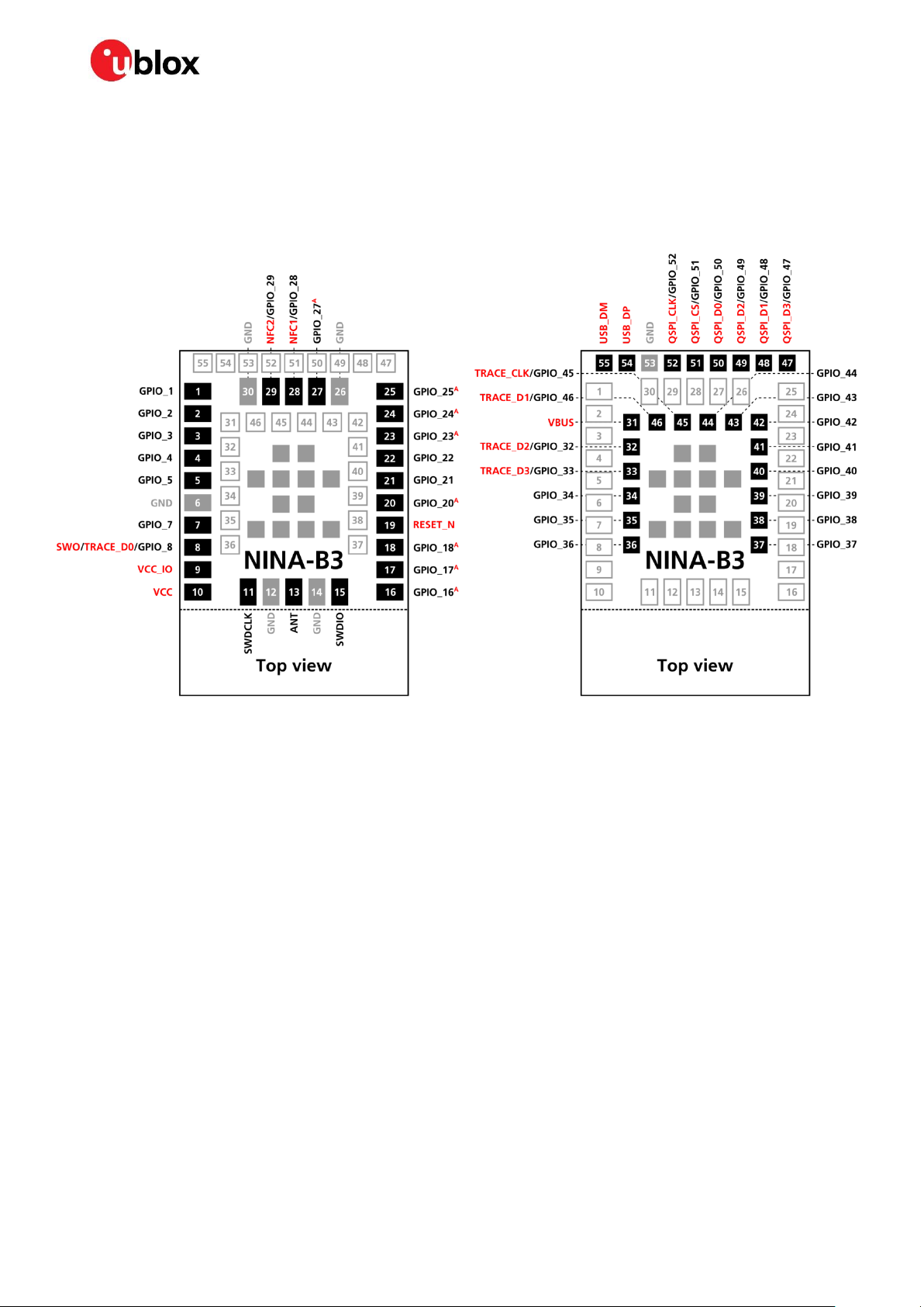
3.1 NINA-B30 series pin assignment
The pin-out described in Figure 3 is an example assignment that shows the module in an
unconfigured state.
A = Analog function capable pin
Figure 3: NINA-B30 series pin assignment (top view)
The grey pins in the center of the modules are GND pins. The outline of NINA-B301 ends at the
dotted line as shown in Figure 3, where the antenna area of the NINA-B302 begins.
☞ Most of the digital or analog functions described in this data sheet may be freely assigned to any
GPIO pin. Analog functions are limited to analog capable pins. Signals that are highlighted in red
in Figure 3 are not freely assignable but locked to a specific pin.
☞ The GPIO pins - 16, 17, 18 and 20 are connected to the pins located close to the radio part of the
RF chip. It is recommended to avoid using these pins for high speed digital interfaces or
sinking/sourcing large currents through them. Doing so may affect the RF performance.
⚠ Do not apply an NFC field to the NFC pins when they are configured as GPIOs as this can cause
permanent damage to the module. When driving different logic levels on these pins in the GPIO
mode, a small current leakage will occur. Ensure that they are set to the same logic level before
entering into any power saving modes. See section 4.2.6 for more information.
UBX-17052099 - R02 Pin definition Page 22 of 50
Page 23

NINA-B3 series - Data Sheet
No.
Name
I/O
Description
nRF52 pin
Remarks
1
GPIO_1
I/O
General purpose I/O
P0.13
2 GPIO_2
I/O
General purpose I/O
P0.14
3
GPIO_3
I/O
General purpose I/O
P0.15
4
GPIO_4
I/O
General purpose I/O
P0.16
5 GPIO_5
I/O
General purpose I/O
P0.24
6 GND - Ground
7
GPIO_7
I/O
General purpose I/O
P0.25
8
SWO/TRACE_D0/
GPIO_8
I/O
General purpose I/O
P1.00
May be used for parallel/serial
trace debug
9
VCC_IO
I
Module I/O level voltage input
Must be connected to VCC on
NINA-B3
10
VCC I Module supply voltage input
1.7-3.6 V range
11
SWDCLK
I
Serial Wire Debug port clock signal
SWDCLK
12
GND - Ground
13
ANT
I/O
Tx/Rx antenna interface
50 Ω nominal characteristic
impedance, only used with
NINA-B3x1 modules
14
GND - Ground
15
SWDIO
I/O
Serial Wire Debug port data signal
SWDIO
16
GPIO_16
I/O
Analog function enabled GPIO
P0.03
Pin is analog capable - use as low
drive, low frequency GPIO only
17
GPIO_17
I/O
Analog function enabled GPIO
P0.28
Pin is analog capable - use as low
drive, low frequency GPIO only
18
GPIO_18
I/O
Analog function enabled GPIO
P0.02
Pin is analog capable - use as low
drive, low frequency GPIO only
19
RESET_N
I/O
System reset input
P0.18
Active low
20
GPIO_20
I/O
Analog function enabled GPIO
P0.31
Pin is analog capable - use as low
drive, low frequency GPIO only
21
GPIO_21
I/O
General purpose I/O
P1.12
Use as low drive, low frequency
GPIO only
22
GPIO_22
I/O
General purpose I/O
P1.13
Use as low drive, low frequency
GPIO only
23
GPIO_23
I/O
Analog function enabled GPIO
P0.29
Pin is analog capable - use as low
drive, low frequency GPIO only
24
GPIO_24
I/O
Analog function enabled GPIO
P0.30
Pin is analog capable - use as low
drive, low frequency GPIO only
25
GPIO_25
I/O
Analog function enabled GPIO
P0.04
Pin is analog capable
26
GND - Ground
27
GPIO_27
I/O
Analog function enabled GPIO
P0.05
Pin is analog capable
28
NFC1/GPIO_28
I/O
NFC pin 1 (default)
P0.09
May be used as a GPIO- use as low
drive, low frequency GPIO only
29
NFC2/GPIO_29
I/O
NFC pin 2 (default)
P0.10
May be used as a GPIO - use as
low drive, low frequency GPIO only
30
GND - Ground
31
VBUS
I
USB interface 5 V input
VBUS
Is required for the USB interface to
work
32
TRACE_D2/GPIO_32
I/O
General purpose I/O
P0.11
May be used for parallel trace
debug
33
TRACE_D3/GPIO_33
I/O
General purpose I/O
P1.09
May be used for parallel trace
debug
UBX-17052099 - R02 Pin definition Page 23 of 50
Page 24

NINA-B3 series - Data Sheet
No.
Name
I/O
Description
nRF52 pin
Remarks
34
GPIO_34
I/O
General purpose I/O
P1.08
35
GPIO_35
I/O
General purpose I/O
P1.01
Use as low drive - low frequency
GPIO only
36
GPIO_36
I/O
General purpose I/O
P1.02
Use as low drive - low frequency
GPIO only
37
GPIO_37
I/O
General purpose I/O
P1.03
Use as low drive - low frequency
GPIO only
38
GPIO_38
I/O
General purpose I/O
P1.10
Use as low drive - low frequency
GPIO only
39
GPIO_39
I/O
General purpose I/O
P1.11
Use as low drive - low frequency
GPIO only
40
GPIO_40
I/O
General purpose I/O
P1.15
Use as low drive - low frequency
GPIO only
41
GPIO_41
I/O
General purpose I/O
P1.14
Use as low drive - low frequency
GPIO only
42
GPIO_42
I/O
General purpose I/O
P0.26
43
GPIO_43
I/O
General purpose I/O
P0.06
44
GPIO_44
I/O
General purpose I/O
P0.27
45
TRACE_CLK/GPIO_45
I/O
General purpose I/O
P0.07
May be used for parallel trace
debug
46
TRACE_D1/GPIO_46
I/O
General purpose I/O
P0.12
May be used for parallel trace
debug
47
QSPI_D3/GPIO_47
I/O
General purpose I/O
P0.23
Recommended pin for QSPI_D3
48
QSPI_D1/GPIO_48
I/O
General purpose I/O
P0.21
Recommended pin for QSPI_D1
49
QSPI_D2/GPIO_49
I/O
General purpose I/O
P0.22
Recommended pin for QSPI_D2
50
QSPI_D0/GPIO_50
I/O
General purpose I/O
P0.20
Recommended pin for QSPI_D0
51
QSPI_CS/GPIO_51
I/O
General purpose I/O
P0.17
Recommended pin for QSPI_CS
52
QSPI_CLK/GPIO_52
I/O
General purpose I/O
P0.19
Recommended pin for QSPI_CLK
53
GND - Ground
54
USB_DP
I/O
USB differential data signal
USB_DP
55
USB_DM
I/O
USB differential data signal
USB_DM
EGP - Exposed Ground Pins
The exposed pins in the center of
the module should be connected
to GND
Table 7: NINA-B30 series pin-out
UBX-17052099 - R02 Pin definition Page 24 of 50
Page 25

NINA-B3 series - Data Sheet
3.2 NINA-B31 series pin assignment (with u-blox connectivity
software)
The pin-out as shown in Figure 4 describes the pin configuration used by the u-blox connectivity
software.
Figure 4: NINA-B31 series pin assignment (top view)
The grey pins in the center of the modules are GND pins. The outline of NINA-B311 ends at the dotted
line as shown in Figure 4, where the antenna area of NINA-B312 begins.
⚠ Follow this pin layout when using the u-blox connectivity software. No interfaces can be moved or
added.
⚠ Do not apply an NFC field to the NFC pins when they are configured as GPIOs as it can cause
permanent damage to the module. While using the u-blox connectivity software, these pins will
always be set to the NFC mode. See section 4.2.6 for more information.
UBX-17052099 - R02 Pin definition Page 25 of 50
Page 26

NINA-B3 series - Data Sheet
No.
Name
I/O
Description
Remarks
1
RED O RED system status signal
Active low, should be routed to an RGB LED
2
IO_2
-
u-blox connectivity software (uCS) IO
pin
Can be used for manual digital I/O
3
IO_3 - uCS IO pin
Can be used for manual digital I/O
4
IO_4 - uCS IO pin
Can be used for manual digital I/O
5
IO_5 - uCS IO pin
Can be used for manual digital I/O
6
GND - Ground
7
GREEN/SWITCH_1
I/O
This signal is multiplexed:
GREEN: System status signal.
SWITCH_1: Multiple functions
Active low.
GREEN: Should be routed to an RGB LED.
SWITCH_1: See section 2.8.3 for more
information.
8
BLUE
O
BLUE system status signal
Active low, should be routed to an RGB LED
9
VCC_IO
I
Module I/O level voltage input
Must be connected to VCC on NINA-B3
10
VCC I Module supply voltage input
1.7-3.6 V range
11
RSVD
-
RESERVED pin
Leave unconnected
12
GND - Ground
13
ANT
I/O
Tx/Rx antenna interface
50 Ω nominal characteristic impedance, only
used with NINA-B3x1 modules
14
GND - Ground
15
RSVD
-
RESERVED pin
Leave unconnected
16
UART_DTR
O
UART data terminal ready signal
Used to indicate system status
17
UART_DSR
I
UART data set ready signal
Used to change the system modes
18
SWITCH_2
I
Multiple functions
Active low, see section 2.8.3 for more
information.
19
RESET_N
I
External system reset input
Active low
20
UART_RTS
O
UART request to send control signal
Used only when hardware flow control is enabled
21
UART_CTS
I
UART clear to send control signal
Used only when hardware flow control is enabled
22
UART_TXD
O
UART data output
23
UART_RXD
I
UART data input
24
IO_24
-
uCS IO pin
Can be used for manual digital I/O
25
IO_25
-
uCS IO pin
Can be used for manual digital I/O
26
GND - Ground
27
IO_27
-
uCS IO pin
Can be used for manual digital I/O
28
NFC1
I/O
NFC pin 1
29
NFC2
I/O
NFC pin 2
30
GND - Ground
31
RSVD
-
RESERVED pin
Leave unconnected
32
IO_32
-
uCS IO pin
Can be used for manual digital I/O
33
IO_33
-
uCS IO pin
Can be used for manual digital I/O
34
IO_34
-
uCS IO pin
Can be used for manual digital I/O
35
IO_35
-
uCS IO pin
Can be used for manual digital I/O
36
IO_36
-
uCS IO pin
Can be used for manual digital I/O
37
IO_37
-
uCS IO pin
Can be used for manual digital I/O
38
IO_38
-
uCS IO pin
Can be used for manual digital I/O
39
IO_39
-
uCS IO pin
Can be used for manual digital I/O
40
IO_40
-
uCS IO pin
Can be used for manual digital I/O
41
IO_41
-
uCS IO pin
Can be used for manual digital I/O
UBX-17052099 - R02 Pin definition Page 26 of 50
Page 27

NINA-B3 series - Data Sheet
No.
Name
I/O
Description
Remarks
42
IO_42
-
uCS IO pin
Can be used for manual digital I/O
43
IO_43
-
uCS IO pin
Can be used for manual digital I/O
44
IO_44
-
uCS IO pin
Can be used for manual digital I/O
45
IO_45
-
uCS IO pin
Can be used for manual digital I/O
46
IO_46
-
uCS IO pin
Can be used for manual digital I/O
47
IO_47
-
uCS IO pin
Can be used for manual digital I/O
48
IO_48
-
uCS IO pin
Can be used for manual digital I/O
49
IO_49
-
uCS IO pin
Can be used for manual digital I/O
50
IO_50
-
uCS IO pin
Can be used for manual digital I/O
51
IO_51
-
uCS IO pin
Can be used for manual digital I/O
52
IO_52
-
uCS IO pin
Can be used for manual digital I/O
53
GND - Ground
54
RSVD
-
RESERVED pin
Leave unconnected
55
RSVD
-
RESERVED pin
Leave unconnected
EGP - Exposed Ground Pad
The exposed pads in the center of the module
should be connected to the GND
Table 8: NINA-B3 series and u-blox connectivity software pin-out
UBX-17052099 - R02 Pin definition Page 27 of 50
Page 28

NINA-B3 series - Data Sheet
Symbol
Description
Condition
Min
Max
Unit
VCC
Module supply voltage
Input DC voltage at VCC pin
-0.3
3.9
V
V_DIO
Digital pin voltage
Input DC voltage at any digital I/O pin, VCC ≤ 3.6 V
-0.3
VCC + 0.3
V
Input DC voltage at any digital I/O pin, VCC > 3.6 V
-0.3
3.9 V P_ANT
Maximum power at receiver
Input RF power at antenna pin
+10
dBm
Parameter
Min
Typical
Max
Unit
Remarks
ESD sensitivity for all pins except ANT pin
4
kV
Human body model according to JEDEC JS001
750
V
Charged device model according to JESD22C101
ESD indirect contact discharge
±8
kV
According to EN 301 489-1
Parameter
Min
Max
Unit
Storage temperature
-40
+125
°C
Operating temperature
-40
+85
°C
4 Electrical specifications
⚠ Stressing the device above one or more of the ratings listed in the Absolute maximum rating
section may cause permanent damage. These are stress ratings only. Operating the module at
these or at any conditions other than those specified in the Operating conditions section of this
document should be avoided. Exposure to absolute maximum rating conditions for extended
periods may affect device reliability.
☞ Operating condition ranges define those limits within which the functionality of the device is
guaranteed. Where application information is given, it is advisory only and does not form part of
the specification.
4.1 Absolute maximum ratings
Table 9: Absolute maximum ratings
⚠ The product is not protected against overvoltage or reversed voltages. The voltage spikes
exceeding the power supply voltage specification, provided in Table 9, must be limited to the
values within the specified boundaries by using appropriate protection devices.
4.1.1 Maximum ESD ratings
Table 10: Maximum ESD ratings
⚠ NINA-B3 series modules are Electrostatic Sensitive Devices and require special precautions while
handling. See section 8.4 for ESD handling instructions.
4.2 Operating conditions
☞ Unless otherwise specified, all operating condition specifications are at an ambient temperature
of 25 °C and a supply voltage of 3.3 V.
⚠ Operation beyond the specified operating conditions is not recommended and extended
exposure beyond them may affect device reliability.
4.2.1 Operating temperature range
Table 11: Temperature range
UBX-17052099 - R02 Electrical specifications Page 28 of 50
Page 29

NINA-B3 series - Data Sheet
Symbol
Parameter
Min
Typ
Max
Unit
VCC
Input supply voltage
1.7
3.3
3.6 V t_RVCC
Supply voltage rise time
60
ms
VCC_ripple
VCC input noise peak to peak, 10 - 100 KHz
TBD
mV
VCC input noise peak to peak, 100 KHz - 1 MHz
TBD
mV
VCC input noise peak to peak, 1 - 3 MHz
TBD
mV
VCC_IO
I/O reference voltage
VCC V
Mode
Condition
Typical
Peak
Sleep
No clocks running, no RAM data retention
400 nA
Sleep
No clocks running, 64 kB RAM data retention
880 nA
Sleep
No clocks running, 256 kB RAM data retention
2.3 µA
Standby
RTC and 64 kB RAM data retention. System running on 32.768 kHz clock from crystal.
1.3 µA
Active
CPU running benchmarking tests @ 64 MHz clock speed, all interfaces idle
3.6 mA
Active
Radio RX only
4.8 mA
Active
Radio TX only, 0 dBm output power
4.9 mA
Active
Radio TX only, +8 dBm output power
14.1 mA
Active
CPU running benchmarking tests @ 64 MHz clock speed, Radio TX 0 dBm output
power
9.1 mA
3.3 V VCC
1.8 V VCC
Mode
Condition
Average
Peak
Average
Peak
Active
Advertising 1 s periods with +8 dBm output power and 31 bytes
payload, CPU and UART interface is running
0.93 mA
20 mA
Standby
Advertising 1 s periods with +8 dBm output power and 31 bytes
payload
50 uA
19 mA
Standby
One advertisement event (4.7 ms), +8 dBm output power and 31
bytes payload
4.9 mA
19 mA
Active
Connected as peripheral, connection events 30 ms periods, +8
dBm output power and 0 bytes payload, CPU and UART interface
is running
0.98 mA
20 mA
Standby
Connected as peripheral, connection events 30 ms periods, +8
dBm output power and 0 bytes payload
110 uA
19 mA
Sleep
UART DSR pin is used to enter the sleep mode. No RAM retention.
400 nA
4 mA
4.2.2 Supply/Power pins
Table 12: Input characteristics of voltage supply pins
4.2.3 Current consumption
Table 13 shows the typical current consumption of a NINA-B3 module, independent of the software
used.
Table 13: Module VCC current consumption
Table 14 shows the current consumption during some typical use cases when using the u-blox
connectivity software:
Table 14: Current consumption during typical use cases
UBX-17052099 - R02 Electrical specifications Page 29 of 50
Page 30

NINA-B3 series - Data Sheet
Parameter
Test condition
Min
Typ
Max
Unit
Receiver input sensitivity
Conducted at 25 °C, 1 Mbit/s BLE mode
-94 dBm
Conducted at 25 °C, 2 Mbit/s BLE mode
-91 dBm
Conducted at 25 °C, 500 kbit/s BLE mode
-97 dBm
Conducted at 25 °C, 125 kbit/s BLE mode
-100 dBm
Maximum output power
Conducted at 25 °C
+8 dBm
Pin name
Parameter
Min
Typ
Max
Unit
Remarks
RESET_N
Low-level input
0 0.3*VCC
V
Internal pull-up resistance
13 kΩ
RESET duration
55
ms
Time taken to release a pin reset.
Pin name
Parameter
Min
Typ
Max
Unit
Remarks
Any digital
pin
Input characteristic:
Low-level input
0 0.3*VCC
V
Input characteristic:
high-level input
0.7*VCC
VCC V
Output characteristic:
Low-level output
0 0.4 V Normal drive strength
0 0.4 V High drive strength
Output characteristic:
High-level output
VCC-0.4
VCC V Normal drive strength
VCC-0.4
VCC V High drive strength
Input pull-up resistance
13 kΩ
Can be added to any GPIO pin
configured as input
Input pull-down resistance
13 kΩ
Can be added to any GPIO pin
configured as input
GPIO_28,
GPIO_29
Leakage current
1 4
µA
When not configured for NFC and
driven to different logic levels
Symbol
Parameter
Bus capacitance
Min
Typ
Max
Unit
R_PUstandard
External pull-up resistance required on
I2C interface in standard mode (100
Kbps)
10 pF
1 - 115
kΩ
50 pF
1 - 23
kΩ
200 pF
1 - 6
kΩ
400 pF
1 - 3
kΩ
R_PUfast
External pull-up resistance required on
I2C interface in fast mode (400 Kbps)
10 pF
1 - 35
kΩ
50 pF
1 - 7
kΩ
200 pF
1 - 1.5
kΩ
400 pF
1 - 1
kΩ
4.2.4 RF performance
Table 15: RF performance
4.2.5 RESET_N pin
Table 16: RESET_N pin characteristics
4.2.6 Digital pins
Table 17: Digital pin characteristics
4.2.7 I
Table 18: Suggested pull-up resistor values
UBX-17052099 - R02 Electrical specifications Page 30 of 50
2
C pull-up resistor values
Page 31

NINA-B3 series - Data Sheet
Symbol
Parameter
Min
Typ
Max
Unit
I_powersave
Current consumption when the comparator is in ‘power save’
mode
2
µA
I_balenced
Current consumption when the comparator is in ‘balanced’ mode
5
µA
I_speed
Current consumption when the comparator is in ‘high speed’
mode
10 µA
I_lowpower
Current consumption of the low power comparator
0.5 µA
t_powersave
Time to generate interrupt/event when the comparator is in
‘power save’ mode
0.6 µs
t_balanced
Time to generate interrupt/event when the comparator is in
‘balanced’ mode
0.2 µs
t_speed
Time to generate interrupt/event when the comparator is in
‘high speed’ mode
0.1 µs
t_lowpower
Time to generate interrupt/event for the low power comparator
5
µs
4.2.8 Analog comparator
Table 19: Electrical specification of the two analog comparators
UBX-17052099 - R02 Electrical specifications Page 31 of 50
Page 32
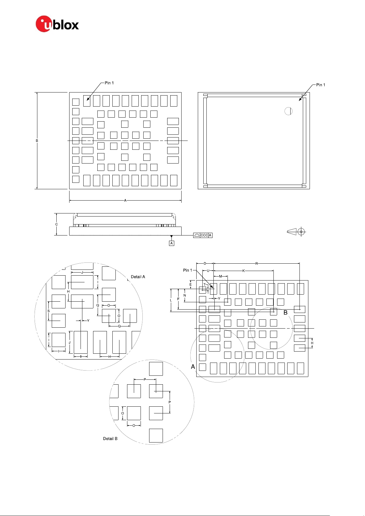
NINA-B3 series - Data Sheet
5 Mechanical specifications
5.1 NINA-B3x1 Mechanical specification
Figure 5: NINA-B3x1 mechanical outline
Figure 6: NINA-B3 detailed dimensions
UBX-17052099 - R02 Mechanical specifications Page 32 of 50
Page 33

NINA-B3 series - Data Sheet
Parameter
Description
Typical [mm]
[mil]
Tolerance [mm]
[mil]
A
Module PCB length
11.6
B
Module PCB width
10.0 C
Module thickness
2.23
ccc
Seating plane coplanarity
0.10
D
Horizontal edge to pin no. 1 center
1.80 E
Vertical edge to pin no. 1 center
0.875
F
Vertical pin no. 1 center to lateral pin center
2.125
H
Lateral and antenna row pin to pin pitch
1.00 I
Lateral, antenna row and outer pin width
0.70
J
Lateral and antenna row pin length
1.15
K
Horizontal pin no. 1 center to central pin center
6.225
L Vertical pin no. 1 center to central pin center
2.40
M
Horizontal pin no. 1 center to inner row pin center
1.45
N
Vertical pin no. 1 center to inner row pin center
1.375
O Central, inner and outer row pin width and length
0.70
P
Central pin to central pin pitch
1.15
Q
Inner row pin to pin pitch
1.10 R
Horizontal pin no. 1 center to antenna row pin center
8.925
S
Outer row pin to pin pitch
1.0
T
Vertical pin no. 1 center to outer row pin center
0.125
U Horizontal pin no. 1 center to outer row pin center
1.15
Y
Horizontal pin no. 1 center to lateral pin center
0.075
Module weight [g]
<1.0
Table 20: NINA-B3x1 mechanical outline data
UBX-17052099 - R02 Mechanical specifications Page 33 of 50
Page 34
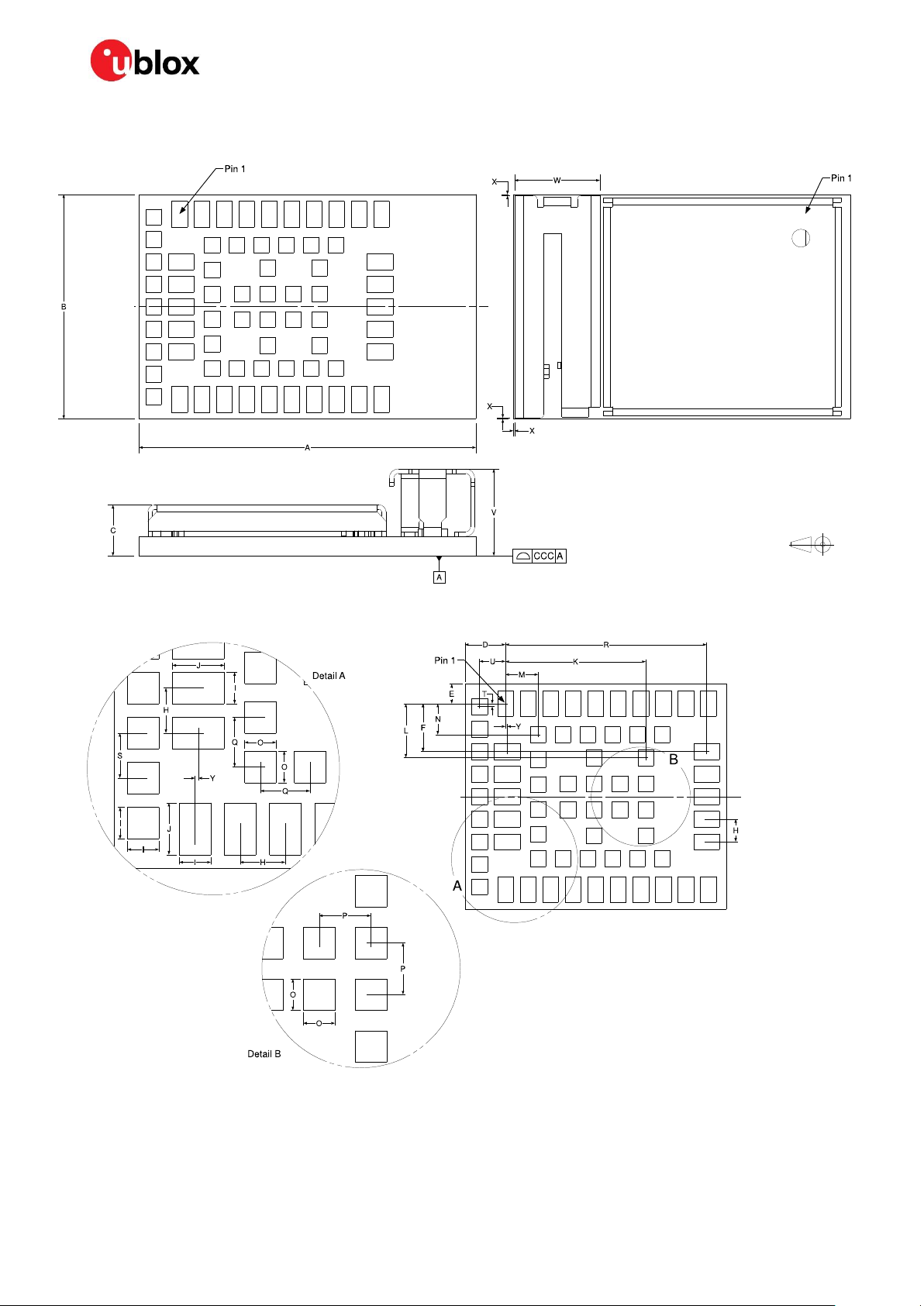
NINA-B3 series - Data Sheet
5.2 NINA-B3X2 Mechanical specifications
Figure 7: NINA-B3X2 mechanical outline
Figure 8: NINA-B3 detailed dimensions
UBX-17052099 - R02 Mechanical specifications Page 34 of 50
Page 35

NINA-B3 series - Data Sheet
Parameter
Description
Typical [mm]
[mil]
Tolerance [mm]
[mil]
A
Module PCB length
15.0 B
Module PCB width
10.0 C
Module thickness
2.23 ccc
Seating plane coplanarity
0.10 D
Horizontal edge to pin no. 1 center
1.80 E
Vertical edge to pin no. 1 center
0.875
F Vertical pin no. 1 center to lateral pin center
2.125
H Lateral and antenna row pin to pin pitch
1.00 I
Lateral, antenna row and outer pin width
0.70 J
Lateral and antenna row pin length
1.15 K
Horizontal pin no. 1 center to central pin center
6.225
L Vertical pin no. 1 center to central pin center
2.40 M
Horizontal pin no. 1 center to inner row pin center
1.45 N
Vertical pin no. 1 center to inner row pin center
1.375
O Central, inner and outer row pin width and length
0.70 P
Central pin to central pin pitch
1.15 Q
Inner row pin to pin pitch
1.10 R
Horizontal pin no. 1 center to antenna row pin center
8.925
S Outer row pin to pin pitch
1.0 T
Vertical pin no. 1 center to outer row pin center
0.125
U Horizontal pin no. 1 center to outer row pin center
1.15 V
PCB and antenna thickness
3.83 W
Module antenna width
3.8 X
Antenna overhang outside module outline on any side
0.0 +0.60
Y Horizontal pin no. 1 center to lateral pin center
0.075
Module weight [g]
<1.0
Table 21: NINA-B3X2 mechanical outline data
UBX-17052099 - R02 Mechanical specifications Page 35 of 50
Page 36

NINA-B3 series - Data Sheet
6 Qualification and approvals
6.1 Country approvals
The NINA-B3 module series is certified for use in the following countries/regions:
USA (FCC)
Canada (IC)
See the following sections for additional information.
☞ Further country approvals are pending.
6.2 FCC/IC Compliance
This device complies with Part 15 of the FCC Rules and with Industry Canada license-exempt RSS
standard(s).
6.2.1 Open CPU responsibility and obligations
⚠ Note that the FCC/IC modular transmitter approvals for NINA-B30 only allow u-blox AG to
integrate the module into an end-product. The integration of the module into an end-product can
only be made by the grantee himself. To allow someone else to integrate NINA-B30 into an endproduct, u-blox AG will help the integrator to obtain the status as grantee. The status as grantee
is obtained by performing a “change in ID”/”Multiple listing”.
The term “Change in ID” relates to § 2.933 of Title 47 of the Code of Federal Regulations (CFR) and
the term Multiple listing relates to section 8.4 of Radio Standards Procedure RSP-100.
Please contact u-blox support for more information regarding the “Change in ID”/”Multiple listing”
process.
⚠ Any changes or modifications NOT explicitly APPROVED by the grantee may cause the module to
cease to comply with the FCC rules part 15 thus void the user’s authority to operate the
equipment.
UBX-17052099 - R02 Qualification and approvals Page 36 of 50
Page 37

NINA-B3 series - Data Sheet
6.2.1.1 FCC Compliance
The NINA-B3 modules are for OEM integrations only. The end-product will be professionally installed
in such manner that only the authorized antennas can be used.
For NINA-B301 and NINA-B311, an external antenna connector (U.FL. connector) reference design is
available and must be followed to comply with the NINA-B30/NINA-B31 FCC/IC modular approval
(see the NINA-B3 Series System Integration Manual [3]).
6.2.1.2 FCC statement
This device complies with Part 15 of the FCC Rules. Operation is subject to the following two
conditions:
1. This device may not cause harmful interference, and
2. This device must accept any interference received, including interference that may cause
undesired operation.
This equipment has been tested and found to comply with the limits for a Class B digital
device, pursuant to Part 15 of the FCC Rules. These limits are designed to provide reasonable
protection against harmful interference in a residential installation. This equipment
generates, uses and can radiate radio frequency energy and, if not installed and used in
accordance with the instructions, may cause harmful interference to radio communications.
However, there is no guarantee that the interference will not occur in a particular installation.
If this equipment does cause harmful interference to radio or television reception, which can
be determined by turning the equipment off and on, the user is encouraged to try to correct
the interference by one or more of the following measures:
Reorient or relocate the receiving antenna
Increase the separation between the equipment and receiver
Connect the equipment into an outlet on a circuit different from that to which the
receiver is connected.
Consult the dealer or an experienced radio/TV technician for help.
6.2.2 RF-exposure statement
6.2.2.1 IC Compliance
This equipment complies with the requirements of IC RSS-102 issue 5 radiation exposure limits set
forth for an uncontrolled environment.
Having a separation distance of minimum 15 mm between the user and/or bystander and the
antenna and /or radiating element ensures that the output power (e.i.r.p.) of NINA-B3 is below the
SAR evaluation Exemption limits defined in RSS-102 issue 5.
6.2.2.2 FCC Compliance
This device complies with the FCC radiation exposure limits set forth for an uncontrolled
environment.
Having a separation distance of minimum 10 mm between the user and/or bystander and the
antenna and /or radiating element ensures that max output power of NINA-B3 is below the SAR test
exclusion limits presented in KDB 447498 D01v06.
UBX-17052099 - R02 Qualification and approvals Page 37 of 50
Page 38

NINA-B3 series - Data Sheet
6.2.3 End-product user manual instructions
6.2.3.1 IC Compliance
☞ User manuals for license-exempt radio apparatus shall contain the following text, or an
equivalent notice that shall be displayed in a conspicuous location, either in the user manual or
on the device, or both:
This device complies with Industry Canada’s license-exempt RSSs. Operation is subject to the
following two conditions:
(1) This device may not cause interference; and
(2) This device must accept any interference, including interference that may cause undesired
operation of the device.
Under Industry Canada regulations, this radio transmitter can only operate using an antenna of a
type and maximum (or lesser) gain approved for the transmitter by Industry Canada. To reduce
potential radio interference to other users, the antenna type and its gain should be chosen in such a
way that the equivalent isotropically radiated power (e.i.r.p.) is not more than that is necessary for
successful communication.
☞ Le manuel d’utilisation des appareils radio exempts de licence doit contenir l’énoncé qui suit, ou
l’équivalent, à un endroit bien en vue dans le manuel d’utilisation ou sur l’appareil,
ou encore aux deux endroits.
Le présent appareil est conforme aux CNR d’Industrie Canada applicables aux appareils radio
exempts de licence. L’exploitation est autorisée aux deux conditions suivantes:
(1) l’appareil ne doit pas produire de brouillage;
(2) l’utilisateur de l’appareil doit accepter tout brouillage radioélectrique subi, même si le
brouillage est susceptible d’en compromettre le fonctionnement.
Conformément aux réglementations d’Industry Canada, cet émetteur radio ne peut fonctionner qu’à
l’aide d’une antenne dont le type et le gain maximal (ou minimal) ont été approuvés pour cet
émetteur par Industry Canada. Pour réduire le 25ecess d’interférences avec d’autres utilisateurs, il
faut choisir le type d’antenne et son gain de telle sorte que la puissance isotrope rayonnée
équivalente (p.i.r.e) ne soit pas supérieure à celle requise pour obtenir une communication
satisfaisante.
6.2.4 End-product labeling requirements
6.2.4.1 IC Compliance
The host product shall be properly labelled to identify the modules within the host product.
The Innovation, Science and Economic Development Canada certification label of a module shall be
clearly visible at all times when installed in the host product; otherwise, the host product must be
labelled to display the Innovation, Science and Economic Development Canada certification number
for the module, preceded by the word “Contains” or similar wording expressing the same meaning,
as shown in figure Figure 9.
Le produit hôte devra être correctement étiqueté, de façon à permettre l’identification des modules
qui s’y trouvent.
L’étiquette d’homologation d’un module d’Innovation, Sciences et Développement économique
Canada devra être posée sur le produit hôte à un endroit bien en vue, en tout temps. En l’absence
d’étiquette, le produit hôte doit porter une étiquette sur laquelle figure le numéro d’homologation du
UBX-17052099 - R02 Qualification and approvals Page 38 of 50
Page 39

NINA-B3 series - Data Sheet
This device contains
FCC ID: XPYNINAB30
IC: 8595A-NINAB30
This device contains
FCC ID: XPYNINAB31
IC: 8595A-NINAB31
Model
FCC ID
ISED Certification Number
NINA-B301
XPYNINAB30
8595A-NINAB30
NINA-B302
XPYNINAB30
8595A-NINAB30
NINA-B311
XPYNINAB31
8595A-NINAB31
NINA-B312
XPYNINAB31
8595A-NINAB31
module d’Innovation, Sciences et Développement économique Canada, précédé du mot « contient »,
ou d’une formulation similaire allant dans le même sens et qui va comme suit:
Figure 9: Example of an end product label containing a NINA-B30 series module
Figure 10: Example of an end product label containing a NINA-B31 series module
6.2.4.2 FCC Compliance
For an end product that uses the NINA-B3 series modules, there must be a label containing, at least,
the information shown in Figure 9 or Figure 10:
The label must be affixed on an exterior surface of the end product such that it will be visible upon
inspection in compliance with the modular approval guidelines developed by the FCC.
☞ In accordance with 47 CFR § 15.19, the end-product shall bear the following statement in a
conspicuous location on the device:
“This device complies with Part 15 of the FCC Rules. Operation is subject to the following two
conditions;
(1)this device may not cause harmful interference, and
(2) this device must accept any interference received, including interference that may cause
undesired operation.”
When the device is so small or for such use that it is not practicable to place the statement above on
it, the information shall be placed in a prominent location in the instruction manual or pamphlet
supplied to the user or, alternatively, shall be placed on the container in which the device is
marketed.
In case, where the final product will be installed in locations where the end-user is not able to see the
FCC ID and/or this statement, the FCC ID and the statement shall also be included in the endproduct manual.
Table 22: FCC and ISED Certification Number for the NINA-B3 series modules
6.2.5 End-product compliance
6.2.5.1 General requirements
Any changes to hardware, hosts or co-location configuration may require new radiated emission
and SAR evaluation and/or testing.
Only authorized antenna(s) may be used.
UBX-17052099 - R02 Qualification and approvals Page 39 of 50
Page 40

NINA-B3 series - Data Sheet
Any notification to the end user about how to install or remove the integrated radio module is
NOT allowed.
The modular transmitter approval of NINA-B3 does not exempt the end-product from being
evaluated against applicable regulatory demands. The evaluation of the end-product shall be
performed with the NINA-B3 module installed and operating in a way that reflects the intended
end-product use case. The upper frequency measurement range of the end product evaluation is
the 5th harmonic of 2.4 GHz as declared in 47 CFR Part 15.33 (b)(1).
The following requirements apply to all products that integrate a radio module:
o Subpart B - UNINTENTIONAL RADIATORS
To verify that the composite device of host and module complies with the
requirements of FCC part 15B the integrator shall perform sufficient measurements
using ANSI 63.4-2014.
o Subpart C - INTENTIONAL RADIATORS
It is required that the integrator carry out sufficient verification measurements using
ANSI 63.10-2013 to validate that the fundamental and out of band emissions of the
transmitter part of the composite device complies with the requirements of FCC part
15C.
When the items listed above are fulfilled the host manufacturer can use the authorization
procedures presented in Table 1 of 47 CFR Part 15.101.
6.2.5.2 Co-location (simultaneous transmission)
If the module is to be co-located with another transmitter, additional measurements for
simultaneous transmission are required.
6.2.5.3 802.15.4 channel map limitation (NINA-B30 series only)
The 2.4 GHz band used by 802.15.4 communications is segmented into 15 channels, ranging from
channel 11 at 2405 MHz to channel 26 at 2480 MHz, with 5 MHz channel spacing. Due to the wide
spectral properties of the 802.15.4 signal, the use of channel 26 results in too much power being
transmitted in the FCC restricted band starting at 2483.5 MHz.
Integrators of the NINA-B30 series will have to make a “change in FCC ID” filing to inherit the test
results of the u-blox FCC compliance tests. In this filing process it must be made clear that the SW
application has been limited to not use channel 26, and that it cannot be ‘unlocked’ by an end-user. It
should also not be possible for an end-user to change the SW on the module to any un-authorized or
modified SW that allows the use of 802.15.4 channel 26.
6.3 Safety Compliance
In order to fulfill the safety standard EN 60950-1, the NINA-B3 series modules must be supplied with
a Class-2 Limited Power Source.
6.4 Bluetooth qualification information
☞ Bluetooth qualifications are pending.
UBX-17052099 - R02 Qualification and approvals Page 40 of 50
Page 41
NINA-B3 series - Data Sheet
Name
U.FL to SMA adapter cable
Connector
U.FL and SMA jack (outer thread and pin receptacle)
Impedance
50 Ω
Minimum cable loss
0.5 dB, The cable loss must be above the minimum
cable loss to meet the regulatory requirements.
Minimum cable length 100 mm.
Comment
The SMA connector can be mounted in a panel.
See the NINA-B3 series System Integration Manual [3]
for information how to integrate the U.FL connector.
Approval
RED, MIC, and NCC
Name
U.FL to Reverse Polarity SMA adapter cable
Connector
U.FL and Reverse Polarity SMA jack (outer thread and
pin) Impedance
50 Ω
Minimum cable loss
0.5 dB, The cable loss must be above the minimum
cable loss to meet the regulatory requirements.
Minimum cable length 100 mm.
Comment
The Reverse Polarity SMA connector can be mounted
in a panel.
See the NINA-B3 series System Integration Manual [3]
for information how to integrate the U.FL connector.
It is required to follow this reference design to comply
with the NINA-B3 FCC/IC modular approvals.
Approval
FCC, IC, RED, MIC, and NCC
NINA-B302 and NINA-B312 (u-blox LILY antenna)
Manufacturer
ProAnt
Gain
+3 dBi
Impedance
50 Ω
Size (HxWxL)
3.0 x 3.8 x 9.9 mm
Type
PIFA
Comment
SMD PIFA antenna on NINA-B302 and NINA-B312. Should not be mounted
inside a metal enclosure.
Approval
FCC, IC, RED, MIC, and NCC
7 Antennas
This chapter provides an overview of the different external antennas that can be used together with
the module.
7.1 Antenna accessories
7.1.1 Single band antennas
UBX-17052099 - R02 Antennas Page 41 of 50
Page 42

NINA-B3 series - Data Sheet
GW.26.0111
Manufacturer
Taoglas
Polarization
Vertical
Gain
+2.0 dBi
Impedance
50 Ω
Size
Ø 7.9 x 30.0 mm
Type
Monopole
Connector
SMA (M) .
Comment
To be mounted on the U.FL to SMA adapter cable.
Approval
RED, MIC, and NCC
Ex-IT 2400 RP-SMA 28-001
Manufacturer
ProAnt
Polarization
Vertical
Gain
+3.0 dBi
Impedance
50 Ω
Size
Ø 12.0 x 28.0 mm
Type
Monopole
Connector
Reverse Polarity SMA plug (inner thread and pin receptacle).
Comment
This antenna requires to be mounted on a metal ground plane for best
performance.
To be mounted on the U.FL to Reverse Polarity SMA adapter cable.
An SMA version antenna is also available but not recommended for use (Ex-IT
2400 SMA 28-001).
Approval
FCC, IC, RED, MIC, and NCC
Ex-IT 2400 MHF 28-001
Manufacturer
ProAnt
Polarization
Vertical
Gain
+2.0 dBi
Impedance
50 Ω
Size
Ø 12.0 x 28.0 mm
Type
Monopole
Cable length
100 mm
Connector
U.FL. connector
Comment
This antenna requires to be mounted on a metal ground plane
for best performance.
To be mounted on a U.FL connector.
See the NINA-B3 series System Integration Manual [3] for
information how to integrate the U.FL connector. It is required
to follow this reference design to comply with the NINA-B3
FCC/IC modular approvals.
Approval
FCC, IC, RED, MIC, and NCC
UBX-17052099 - R02 Antennas Page 42 of 50
Page 43

NINA-B3 series - Data Sheet
Ex-IT 2400 RP-SMA 70-002
Manufacturer
ProAnt
Polarization
Vertical
Gain
+3.0 dBi
Impedance
50 Ω
Size
Ø 10 x 83 mm
Type
Monopole
Connector
Reverse Polarity SMA plug (inner thread and pin receptacle)
Comment
To be mounted on the U.FL to Reverse Polarity SMA adapter cable.
An SMA version antenna is also available but not recommended
for use (Ex-IT 2400 SMA 70-002).
Approval
FCC, IC, RED, MIC, and NCC
InSide-2400
Manufacturer
ProAnt
Gain
+3.0 dBi
Impedance
50 Ω
Size
27 x 12 mm (triangular)
Type
Patch
Cable length
100 mm
Connector
U.FL. connector
Comment
Should be attached to a plastic enclosure or part for best
performance.
To be mounted on a U.FL connector.
See the NINA-B3 series System Integration Manual [3] for
information how to integrate the U.FL connector. It is required to
follow this reference design to comply with the NINA-B3 FCC/IC
modular approvals.
Approval
FCC, IC, RED, MIC, and NCC
FlatWhip-2400 SMA
Manufacturer
ProAnt
Gain
+3.0 dBi
Impedance
50 Ω
Size
Ø 50.0 x 30.0 mm
Type
Monopole
Connector
SMA plug (inner thread and pin)
Comment
To be mounted on the U.FL to SMA adapter cable.
Approval
RED, MIC, and NCC
UBX-17052099 - R02 Antennas Page 43 of 50
Page 44

NINA-B3 series - Data Sheet
FlatWhip-2400 RP-SMA
Manufacturer
ProAnt
Gain
+3.0 dBi
Impedance
50 Ω
Size
Ø 50.0 x 30.0 mm
Type
Monopole
Connector
Reverse Polarity SMA plug (inner thread and pin receptacle).
Comment
To be mounted on the U.FL to SMA adapter cable.
Approval
FCC, IC, RED, MIC, and NCC
UBX-17052099 - R02 Antennas Page 44 of 50
Page 45

NINA-B3 series - Data Sheet
Model
Reel Type
NINA-B3x1
B
NINA-B3x2
A
8 Product handling
8.1 Packaging
The NINA-B3 series modules are delivered as hermetically sealed, reeled tapes to enable efficient
production, production lot set-up and tear-down. For more information about packaging, see the
u-blox Package Information Guide [1]
8.1.1 Reels
The NINA-B3 modules are deliverable in quantities of 500 pieces on a reel. The reel types for the
NINA-B3 modules are provided in Table 23 and detailed information about the reel types are
described in the
Table 23: Reel types for different models of the NINA-B3 series
u-blox Package Information Guide [1].
8.1.2 Tapes
TBD
.
8.2 Moisture sensitivity levels
⚠ The NINA-B3 series modules are Moisture Sensitive Devices (MSD) in accordance with the
IPC/JEDEC specification.
The Moisture Sensitivity Level (MSL) relates to the required packaging and handling precautions.
The NINA-B3 series modules are rated at MSL level 4. For more information regarding moisture
sensitivity levels, labeling and storage, see the
u-blox Package Information Guide [1].
☞ For MSL standards, see IPC/JEDEC J-STD-020, which can be downloaded from www.jedec.org.
8.3 Reflow soldering
Reflow profiles are selected according to u-blox recommendations. See NINA-B3 series System
Integration Manual [3] for more information.
⚠ Failure to observe these recommendations can result in severe damage to the device.
8.4 ESD precautions
⚠ The NINA-B3 series modules contain highly sensitive electronic circuitry and are Electrostatic
Sensitive Devices (ESD). Handling the NINA-B3 series modules without proper ESD protection
may destroy or damage them permanently.
The NINA-B3 series modules are electrostatic sensitive devices (ESD) and require special ESD
precautions typically applied to the ESD sensitive components. Section 4.1.1 provides the maximum
ESD ratings of the NINA-B3 series modules.
Proper ESD handling and packaging procedures must be applied throughout the processing,
handling and operation of any application that incorporates the NINA-B3 series module.
⚠ Failure to observe these recommendations can result in severe damage to the device.
UBX-17052099 - R02 Product handling Page 45 of 50
Page 46

NINA-B3 series - Data Sheet
Reference
Description
1
Date of unit production (year/week)
2
Product version
3
Product name
4
Data Matrix with unique serial number of 19 alphanumeric symbols. The first 3 symbols represent module type
number unique to each module variant, the next 12 symbols represent the unique hexadecimal Bluetooth
address of the module AABBCCDDEEFF, and the last 4 symbols represent the hardware and firmware version
encoded HHFF.
Format
Structure
Product Name
PPPP-TGVV
Ordering Code
PPPP -TGVV-TTQ
Type Number
PPPP -TGVV-TTQ-XX
3 1 2
4
9 Labeling and ordering information
9.1 Product labeling
The labels of the NINA-B3 series modules include important product information as described in this
section.
Figure 15 illustrates the label of the NINA-B3 series modules, which includes the u-blox logo,
production lot, product type number, and certification numbers (if applicable).
Figure 15: Location of product type number on the NINA-B3 series module label
Table 24: NINA-B3 series label description
9.2 Explanation of codes
Three different product code formats are used. The Product Name is used in documentation such as
this data sheet and identifies all u-blox products, independent of packaging and quality grade. The
Ordering Code includes options and quality, while the Type Number includes the hardware and
software versions. Table 25 below details these three different formats:
Table 25: Product code formats
UBX-17052099 - R02 Labeling and ordering information Page 46 of 50
Page 47

NINA-B3 series - Data Sheet
Code
Meaning
Example
PPPP
Form factor
NINA
TG
Platform (Technology and Generation)
T – Dominant technology, for example, W: Wi-Fi, B:
Bluetooth
G - Generation
B3: Bluetooth Generation 3
VV
Variant based on the same platform; range [00…99]
11: default configuration, with antenna pin
TT
Major product version
00: first revision
Q
Quality grade
A: Automotive
B: Professional
C: Standard
B: professional grade
XX
Minor product version (not relevant for certification)
Default value is 00
Ordering Code
Product
NINA-B311-00B
NINA-B3 module with antenna pin, pre-flashed and locked for use with u-blox connectivity software
NINA-B312-00B
NINA-B3 module with internal antenna, pre-flashed and locked for use with u-blox connectivity software
NINA-B301-00B
NINA-B3 module with antenna pin, open CPU for custom applications
NINA-B302-00B
NINA-B3 module with internal antenna, open CPU for custom applications
Table 26 explains the parts of the product code.
Table 26: Part identification code
9.3 Ordering information
Table 27: Product ordering codes
UBX-17052099 - R02 Labeling and ordering information Page 47 of 50
Page 48

NINA-B3 series - Data Sheet
Abbreviation
Definition
ADC
Analog to Digital Converter
BLE
Bluetooth Low Energy
BPF
Band Pass Filter
CTS
Clear To Send
EDM
Extended Data mode
ESD
Electro Static Discharge
FCC
Federal Communications Commission
GATT
Generic ATTribute profile
GPIO
General Purpose Input/Output
IC
Industry Canada
I2C
Inter-Integrated Circuit
MCU
Micro Controller Unit
MSD
Moisture Sensitive Device
QSPI
Quad Serial Peripheral Interface
RTS
Request To Send
SPI
Serial Peripheral Interface
TBD
To be Defined
UART
Universal Asynchronous Receiver/Transmitter
Appendix
A Glossary
Table 28: Explanation of the abbreviations and terms used
UBX-17052099 - R02 Appendix Page 48 of 50
Page 49

NINA-B3 series - Data Sheet
Revision
Date
Name
Comments
R01
10-Nov-2017
ajoh, apet, kgom
Initial release.
R02
10-Sep-2018
ajoh, kgom
Removed Arm Mbed software option. Updated the mechanical specification
(Section 5). Updated RF parameters such as output power and receiver
sensitivity (Table 3). Added current consumption data when running the
u-blox connectivity software (Table 14).
Related documents
[1] u-blox Package Information Guide, document number UBX-14001652
[2] u-blox Short Range AT Commands Manual, document number UBX-14044127
[3] NINA-B3 Series System Integration Manual, document number UBX-15026175
[4] NINA-B3 Getting Started, document number UBX-18022394
☞ For regular updates to u-blox documentation and to receive product change notifications,
register on our homepage (www.u-blox.com).
Revision history
UBX-17052099 - R02 Related documents Page 49 of 50
Page 50

NINA-B3 series - Data Sheet
u-blox Offices
North, Central and South America
u-blox America, Inc.
Phone: +1 703 483 3180
E-mail: info_us@u-blox.com
Regional Office West Coast:
Phone: +1 408 573 3640
E-mail: info_us@u-blox.com
Technical Support:
Phone: +1 703 483 3185
E-mail: support@u-blox.com
Headquarters
Europe, Middle East, Africa
u-blox AG
Phone: +41 44 722 74 44
E-mail: info@u-blox.com
Support: support@u-blox.com
Asia, Australia, Pacific
u-blox Singapore Pte. Ltd.
Phone: +65 6734 3811
E-mail: info_ap@u-blox.com
Support: support_ap@u-blox.com
Regional Office Australia:
Phone: +61 2 8448 2016
E-mail: info_anz@u-blox.com
Support: support_ap@u-blox.com
Regional Office China (Beijing):
Phone: +86 10 68 133 545
E-mail: info_cn@u-blox.com
Support: support_cn@u-blox.com
Regional Office China (Chongqing):
Phone: +86 23 6815 1588
E-mail: info_cn@u-blox.com
Support: support_cn@u-blox.com
Regional Office China (Shanghai):
Phone: +86 21 6090 4832
E-mail: info_cn@u-blox.com
Support: support_cn@u-blox.com
Regional Office China (Shenzhen):
Phone: +86 755 8627 1083
E-mail: info_cn@u-blox.com
Support: support_cn@u-blox.com
Regional Office India:
Phone: +91 80 405 092 00
E-mail: info_in@u-blox.com
Support: support_in@u-blox.com
Regional Office Japan (Osaka):
Phone: +81 6 6941 3660
E-mail: info_jp@u-blox.com
Support: support_jp@u-blox.com
Regional Office Japan (Tokyo):
Phone: +81 3 5775 3850
E-mail: info_jp@u-blox.com
Support: support_jp@u-blox.com
Regional Office Korea:
Phone: +82 2 542 0861
E-mail: info_kr@u-blox.com
Support: support_kr@u-blox.com
Regional Office Taiwan:
Phone: +886 2 2657 1090
E-mail: info_tw@u-blox.com
Support: support_tw@u-blox.com
Contact
For complete contact information, visit us at www.u-blox.com.
UBX-17052099 - R02 Contact Page 50 of 50
 Loading...