

Page 1

Abstract
NINA-B3 series
Stand-alone Bluetooth 5 low energy modules
System integration manual
This document describes the system integration of the NINA-B3 series stand-alone Bluetooth 5 low
energy modules.
UBX-17056748 - R11
C1-Public www.u-blox.com
Page 2

NINA-B3 series - System integration manual
u-blox or third parties may hold intellectual property rights in the products, names, logos and designs included in this
document. Copying, reproduction, modification or disclosure to third parties of this document or any part thereof is only
permitted with the express written permission of u
The information contained herein is provided “as is” and u
implied, is given, including but not limited to, with respect to the accuracy, correctness, reliability and fitness for a par
purpose of the information. This document may be revised by u
documents, visit www.u
Copyright © u
Document information
Title NINA-B3 series
Subtitle Stand-alone Bluetooth 5 low energy modules
Document type System integration manual
Document number UBX-17056748
Revision and date R11 8-Dec-2020
Disclosure restriction C1-Public
Product status
Functional Sample Draft For functional testing. Revised and supplementary data will be published later.
In Development /
Prototype
Engineering Sample Advance Information Data based on early testing. Revised and supplementary data will be published later.
Initial Production Early Production Information Data from product verification. Revised and supplementary data may be published later.
Mass Production /
End of Life
Corresponding content status
Objective Specification Target values. Revised and supplementary data will be published later.
Production Information Document contains the final product specification.
This document applies to the following products:
Open CPU:
Product name Type Number Product status
NINA-B301 NINA-B301-00B Early Production Information
NINA-B302 NINA-B302-00B Early Production Information
NINA-B306 NINA-B306-00B Early Production Information
NINA-B306 NINA-B306-01B Early Production Information Without external LFXO.
Comment
u-connectXpress:
Product name Type Number Product status
NINA-B311 NINA-B311-0xB Early Production Information x = SW version
NINA-B312 NINA-B312-0xB Early Production Information ‘’
NINA-B316 NINA-B316-0xB Early Production Information ‘’
Comment
UBX-17056748 - R11 Document information Page 2 of 67
C1-Public
-blox AG.
-blox.com.
-blox.
-blox assumes no liability for its use. No warranty, either express or
-blox at any time without notice. For the most recent
ticular
Page 3

NINA-B3 series - System integration manual
Contents
Document information ............................................................................................................................. 2
Contents ....................................................................................................................................................... 3
1 System description ............................................................................................................................ 6
1.1 Overview and applications ........................................................................................................................ 6
1.2 Architecture ................................................................................................................................................. 9
1.2.1 Block diagrams .................................................................................................................................... 9
1.2.2 Hardware options ............................................................................................................................... 9
1.2.3 Software options ................................................................................................................................ 9
1.3 Pin configuration and function ................................................................................................................. 9
1.4 Supply interfaces ...................................................................................................................................... 10
1.4.1 Main supply input ............................................................................................................................. 10
1.4.2 Digital I/O interfaces reference voltage (VCC_IO) ...................................................................... 10
1.4.3 VCC application circuits .................................................................................................................. 10
1.5 System function interfaces .................................................................................................................... 11
1.5.1 Module reset ...................................................................................................................................... 11
1.5.2 Internal temperature sensor .......................................................................................................... 11
1.6 Debug – Serial Wire Debug (SWD) ......................................................................................................... 11
1.7 Serial interfaces ........................................................................................................................................ 11
1.7.1 Universal Asynchronous Serial Interface (UART) ...................................................................... 11
1.7.2 Serial Peripheral Interface (SPI) ..................................................................................................... 12
1.7.3 Quad serial peripheral interface (QSPI) ........................................................................................ 12
1.7.4 I2C interface ....................................................................................................................................... 13
1.7.5 USB 2.0 interface .............................................................................................................................. 13
1.8 GPIO pins ..................................................................................................................................................... 13
1.8.1 Analog interfaces .............................................................................................................................. 14
1.9 Antenna interfaces ................................................................................................................................... 15
1.9.1 Antenna pin – NINA-B3x1 ................................................................................................................ 15
1.9.2 Integrated antenna – NINA-B3x2/B3x6........................................................................................ 16
1.9.3 NFC antenna ...................................................................................................................................... 16
1.10 Reserved pins (RSVD) .............................................................................................................................. 16
1.11 GND pins ..................................................................................................................................................... 16
2 Software ............................................................................................................................................. 17
2.1 u-connectXpress software ...................................................................................................................... 17
2.2 Open CPU .................................................................................................................................................... 17
2.2.1 Nordic SDK ......................................................................................................................................... 17
2.2.2 Bluetooth MAC address and other production data ................................................................. 22
2.3 Flashing the NINA-B31 u-blox software ............................................................................................... 22
2.3.1 UART flashing ................................................................................................................................... 22
2.4 Flashing the NINA-B30 open CPU software ........................................................................................ 26
2.4.1 SWD flashing ..................................................................................................................................... 26
UBX-17056748 - R11 Contents Page 3 of 67
C1-Public
Page 4

NINA-B3 series - System integration manual
3 Design-in ............................................................................................................................................. 28
3.1 Overview ...................................................................................................................................................... 28
3.2 Design for NINA family ............................................................................................................................. 28
3.3 Antenna interface ..................................................................................................................................... 28
3.3.1 RF transmission line design (NINA-B3x1 only) ........................................................................... 29
3.3.2 Antenna design (NINA-B3x1 only) ................................................................................................. 30
3.3.3 On-board antenna ............................................................................................................................. 33
3.4 Supply interfaces ...................................................................................................................................... 35
3.4.1 Module supply design ...................................................................................................................... 35
3.5 Serial interfaces ........................................................................................................................................ 36
3.5.1 Asynchronous serial interface (UART) design ............................................................................ 36
3.5.2 Serial peripheral interface (SPI) ..................................................................................................... 36
3.5.3 I2C interface ....................................................................................................................................... 36
3.5.4 QSPI interface .................................................................................................................................... 36
3.5.5 USB interface ..................................................................................................................................... 36
3.6 NFC interface ............................................................................................................................................. 36
3.6.1 Battery protection ............................................................................................................................ 37
3.7 General High Speed layout guidelines .................................................................................................. 37
3.7.1 General considerations for schematic design and PCB floor-planning ................................. 37
3.7.2 Module placement ............................................................................................................................ 38
3.7.3 Layout and manufacturing ............................................................................................................. 38
3.8 Module footprint and paste mask ......................................................................................................... 38
3.9 Thermal guidelines ................................................................................................................................... 39
3.10 ESD guidelines ........................................................................................................................................... 39
4 Handling and soldering ................................................................................................................... 40
4.1 Packaging, shipping, storage and moisture preconditioning .......................................................... 40
4.2 Handling ...................................................................................................................................................... 40
4.3 Soldering ..................................................................................................................................................... 40
4.3.1 Reflow soldering process ................................................................................................................ 40
4.3.2 Cleaning .............................................................................................................................................. 41
4.3.3 Other remarks ................................................................................................................................... 42
5 Regulatory information and requirements ............................................................................... 43
5.1 ETSI – European market .......................................................................................................................... 43
5.1.1 Compliance statement .................................................................................................................... 43
5.1.2 NINA-B3 Software security considerations ................................................................................ 43
5.1.3 Output power limitation .................................................................................................................. 43
5.1.4 Safety Compliance ........................................................................................................................... 44
5.2 FCC/ISED – US/Canadian markets ........................................................................................................ 45
5.2.1 Compliance statements .................................................................................................................. 45
5.2.2 RF Exposure ....................................................................................................................................... 45
5.2.3 Antenna selection ............................................................................................................................. 46
5.2.4 IEEE 802.15.4 channel map limitation ......................................................................................... 46
UBX-17056748 - R11 Contents Page 4 of 67
C1-Public
Page 5

NINA-B3 series - System integration manual
5.2.5 Change in ID/Multiple Listing process .......................................................................................... 46
5.2.6 End product verification requirements ........................................................................................ 47
5.2.7 End product labelling requirements ............................................................................................. 47
5.2.8 End product user manual requirements ...................................................................................... 48
5.3 MIC - Japanese market ............................................................................................................................ 49
5.3.1 Compliance statement .................................................................................................................... 49
5.3.2 48-bit address requirement ........................................................................................................... 49
5.3.3 End product labelling requirement................................................................................................ 50
5.3.4 End product user manual requirement ........................................................................................ 50
5.4 NCC – Taiwanese market ........................................................................................................................ 50
5.4.1 Compliance statements .................................................................................................................. 50
5.4.2 End product labelling requirement................................................................................................ 51
5.5 KCC – South Korean market ................................................................................................................... 52
5.5.1 Compliance statement .................................................................................................................... 52
5.5.2 End product labeling requirements .............................................................................................. 52
5.5.3 End product user manual requirements ...................................................................................... 53
5.6 Anatel Brazil compliance ......................................................................................................................... 53
5.7 Australia and New Zealand regulatory compliance ........................................................................... 53
5.8 South Africa regulatory compliance ..................................................................................................... 54
5.9 Integration checklist ................................................................................................................................ 54
5.10 Pre-approved antennas list ..................................................................................................................... 55
5.10.1 Antenna accessories ........................................................................................................................ 56
5.10.2 Single band antennas ...................................................................................................................... 56
6 Product testing ................................................................................................................................. 59
6.1 u-blox In-Series production test ............................................................................................................. 59
6.2 OEM manufacturer production test ..................................................................................................... 59
6.2.1 “Go/No go” tests for integrated devices ...................................................................................... 60
Appendix .................................................................................................................................................... 61
A Glossary .............................................................................................................................................. 61
B Antenna reference designs ........................................................................................................... 62
B.1 Reference design for external antennas (U.FL connector) .................................................. 62
B.1.1 Floor plan .................................................................................................................................... 63
B.1.2 RF trace specification ............................................................................................................ 63
Related documents ................................................................................................................................ 65
Revision history ....................................................................................................................................... 66
Contact ....................................................................................................................................................... 67
UBX-17056748 - R11 Contents Page 5 of 67
C1-Public
Page 6

NINA-B3 series - System integration manual
art power performance.
B30 are open CPU modules that enable customer applications to run on the
class capacity
B302 comes with an internal PIFA antenna,
integrated in the module PCB. The internal antennas are
specifically designed for the small NINA form factor and provides an extensive range, independent of
flashed.
e,
all configurable
B31x modules provide top grade security, thanks to secure
B312 comes with an internal PIFA antenna,
B16 has an internal PCB antenna integrated in the module PCB. The internal antennas are
mall NINA form factor and provides an extensive range, independent of
1 System description
1.1 Overview and applications
The NINA-B3 series modules are small stand-alone Bluetooth 5 low energy microcontroller unit (MCU)
modules. The NINA-B3 features full Bluetooth 5, a powerful Arm
®
Cortex®-M4 with FPU, and state-ofthe-art power performance. The embedded low power crystal in the NINA-B3 series improves power
consumption by enabling optimal power save modes.
The NINA-B3x2 comes with an internal antenna, while the NINA-B3x1 has a pin for use with an
external antenna. The internal PIFA antenna is specifically designed for the small NINA form factor
and provides an extensive range, independent of ground plane and component placement. The
NINA-B3 series is globally certified for use with the internal antenna or a range of external antennas.
This greatly reduces time, cost, and effort for customers integrating the NINA-B3 in their designs.
The NINA-B3 series includes the following two sub-series as listed in the table below:
Model
NINA-B30 series Bluetooth 5 module with a powerful Arm Cortex-M4 with FPU, and state-of-the-
NINA-B31 series Bluetooth 5 module with a powerful Arm Cortex-M4 with FPU and u-connectXpress software pre-
Description
Both the variants of NINAbuilt-in Arm Cortex-M4 with FPU. With 1 MB flash and 256 kB RAM, they offer the best-infor customer applications on top of the Bluetooth low energy stack.
NINA-B301 has a pin for use with an external antenna, NINAand NINA-B06 has an internal PCB antenna
ground plane and component placement.
The NINA-B306-01B module variant comes without the LFXO (Low frequency crystal oscillator) mounted.
The software in NINA-B31 modules provides support for u-blox Bluetooth low energy Serial Port Servic
GATT client and server, beacons, NFC™, and simultaneous peripheral and central roles –
from a host using AT commands. The NINAboot, which ensures the module only boots up with original u-blox software.
NINA-B311 has a pin for use with an external antenna, NINAand NINAspecifically designed for the s
ground plane and component placement.
UBX-17056748 - R11 System description Page 6 of 67
C1-Public
Page 7

NINA-B3 series - System integration manual
NINA-B301
NINA-B302
NINA-B306
Grade
Automotive
Professional
• • •
Standard
Radio
v5.0 v5.0 v5.0
G G G
Bluetooth output power EIRP
[dBm]
10 10 10
Max range [meters]
1400 1400 1400
NFC for “Touch to Pair”
• • •
Antenna type
p i b
Application software
Open CPU for embedded
customer applications
• • •
Interfaces
UART
SPI
I2C
I
2
S
USB
GPIO pins
38 38 38
AD converters (ADC)
Features
GATT server and client
Throughput [Mbit/s]
1.4 1.4 14
Maximum Bluetooth
connections
20 20 20
Secure boot
Mesh networking
FOTA
G = GATT
p = Antenna pin
i = Internal PIFA antenna
b = Internal PCB antenna
= Feature enabled by HW. The actual
support depends on the open CPU
application SW.
Bluetooth qualif
Bluetooth prof
ication
iles
Table 1: NINA-B30 series main features summary
UBX-17056748 - R11 System description Page 7 of 67
C1-Public
Page 8

NINA-B3 series - System integration manual
NINA-B311
NINA-B312
NINA-B316
Grad
e
Automotive
Professional
• • •
Standard
Radio
v5.0 v5.0 v5.0
G G
G
Bluetooth output power EIRP
[dBm] *
10 10 10
Max range [meters]
*
1400 1400 1400
NFC for “Touch to Pair”
• • •
Antenna type
*
p i b
Application software
u-connectXpress
• • •
u-connectScript
• • •
Interfaces
UART
1 1 1
GPIO pins
28 28 28
Features
AT command interface
• • •
Script engine – JavaScript
• • •
GATT server and client
• • •
Extended Data Mode
• • •
Low Energy Serial Port Service
• • •
Throughput [Mbit/s]
0.8 0.8 0.8
Maximum Bluetooth
connections
8 8 8
Secure boot
• • •
G = GATT p = Antenna pin i = Internal PIFA antenna b = PCB antenna
Bluetooth qualif
Bluetooth prof
ication
iles
⚠ Regulations in the European market require the maximum output power of the radio to be limited.
Table 2: NINA-B31 series main features summary
See Section 5.1 for more information.
UBX-17056748 - R11 System description Page 8 of 67
C1-Public
Page 9
NINA-B3 series - System integration manual
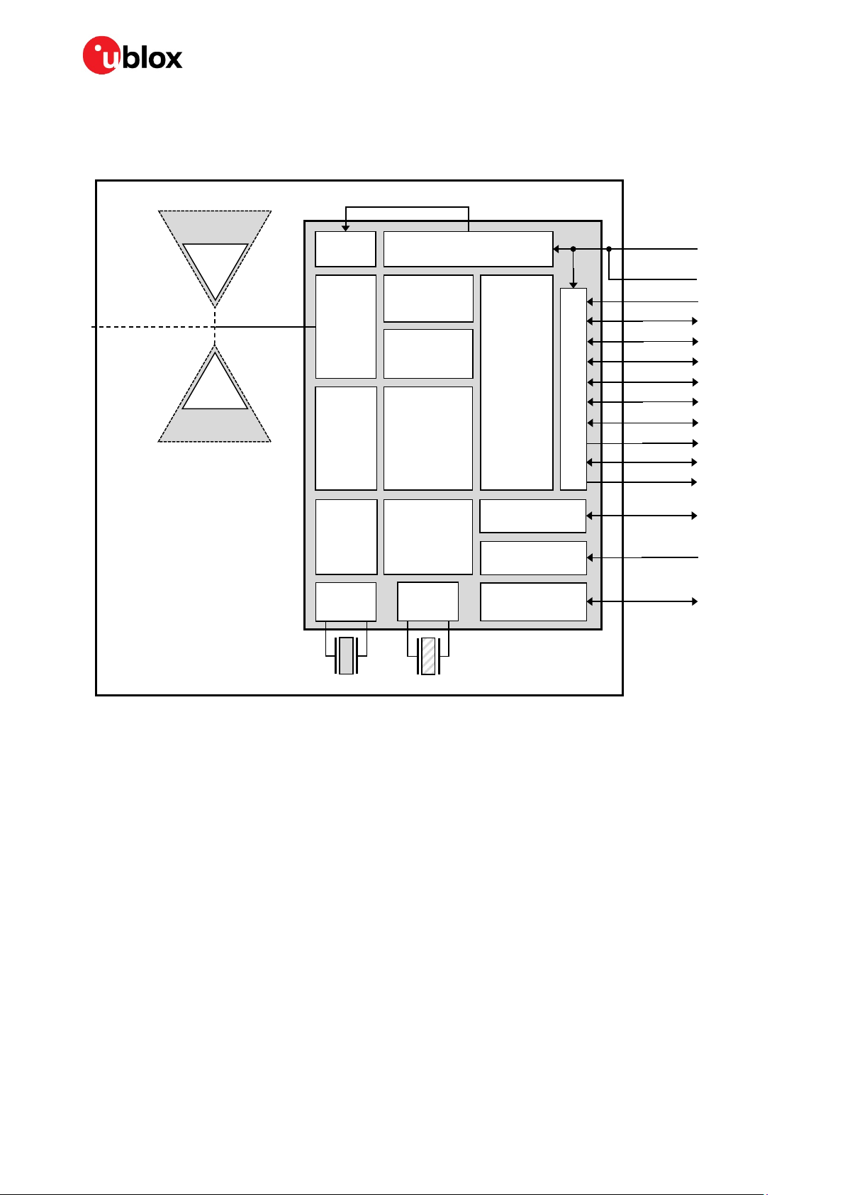
accelerators
VCC_IO (1.7
VCC (1.7
32 MHz
Reset
UART
GPIO
power
I
PWM
I2S
comparator
NFC
nRF52840
QSPI
USB 2.0
QDEC
PDM
CryptoCell
1.2 Architecture
1.2.1 Block diagrams
Antenna pin
NINA-B3x1
PIFA antenna
(NINA-B3x2)
(NINA-B3x6)
PCB trace antenna
1.3 V
System
RF
256 kB
RAM
PLL
DC/DC and LDO regulators
Cryptographic
hardware
BLE baseband
1 MB Flash
RTC, Timers
and Counters
PLL
Nordic Semiconductor
Arm Cortex-M4
USB device
ADC and
Passive NFC tag
- 3.6
– 3.6 V)
SPI
2
C
IO Buffers
Analog
32.768 kHz
Figure 1: Block diagram of the NINA-B3 series. 32.768 kHz crystal not part of NINA-B306-01B
1.2.2 Hardware options
The NINA-B3 series modules use an identical hardware configuration except for the different PCB
sizes and antenna solutions. An on-board 32.768 kHz low power crystal is included in all variants
except the NINA-B306-01B. An integrated DC/DC converter for higher efficiency under heavy load
situations is also included.
1.2.3 Software options
The NINA-B3 series module can be used either together with the pre-flashed u-connectXpress
software or as an open CPU module where you can run your own application developed with the Nordic
SDK development environment inside the NINA-B3 module. The various software options are
described in detail in section 2.
1.3 Pin configuration and function
See the NINA-B3 series Data Sheet [2] for information about pin configuration and function.
UBX-17056748 - R11 System description Page 9 of 67
C1-Public
Page 10

NINA-B3 series - System integration manual
1.4 Supply interfaces
1.4.1 Main supply input
The NINA-B3 series uses an integrated DC/DC converter to transform the supply voltage presented
at the VCC pin into a stable system core voltage. Because of this, the NINA-B3 modules are
compatible for use in battery powered designs.
While using the NINA-B3 with a battery, it is important that the battery type can handle the peak
power of the module. For the battery supply, consider adding extra capacitance on the supply line to
avoid capacity degradation. See the
supply requirements and current consumption.
Rail Voltage requirement Current requirement (peak)
VCC 1.7 V – 3.6 V 20 mA
VCC_IO Tied to VCC
Table 3: Summary of voltage supply requirements
☞ The current requirement in Table 3 considers using the u-connectXpress software with UART
communications. But it does not include any additional I/O current. Any use of external pushbuttons, LEDs, or other interfaces will add to the total current consumption of the NINA-B3
module. The peak current consumption of the entire design will need to be taken into account
when considering a battery powered solution.
NINA-B3 series Data Sheet [2]
for information about voltage
1.4.2 Digital I/O interfaces reference voltage (VCC_IO)
On the NINA-B3 series modules, the I/O voltage level is the same as the supply voltage and VCC_IO is
internally connected to the supply input VCC.
When using NINA-B3 with a battery, the I/O voltage level will vary with the battery output voltage,
depending on the charge of the battery. Level shifters might be needed depending on the I/O voltage
of the host system.
1.4.3 VCC application circuits
The power for NINA-B3 series modules is provided through the VCC pins, which can be one of the
following:
• Switching Mode Power Supply (SMPS)
• Low Drop Out (LDO) regulator
• Battery
The SMPS is the ideal choice when the available primary supply source has a higher value than the
operating supply voltage of the NINA-B3 series modules. The use of SMPS provides the best power
efficiency for the overall application and minimizes the current drawn from the main supply source.
⚠ While selecting SMPS, ensure that the AC voltage ripple at the switching frequency is kept as low
as possible. Layout shall be implemented to minimize impact of high frequency ringing.
The use of an LDO linear regulator is convenient for a primary supply with a relatively low voltage
where the typical 85-90% efficiency of the switching regulator leads to minimal current saving. Linear
regulators are not recommended for high voltage step-down, as they will dissipate a considerable
amount of energy.
DC/DC efficiency should be evaluated as a tradeoff between active and idle duty cycles of the specific
application. Although some DC/DC can achieve high efficiency at extremely light loads, a typical
UBX-17056748 - R11 System description Page 10 of 67
C1-Public
Page 11

NINA-B3 series - System integration manual
DC/DC efficiency quickly degrades as idle current drops below a few mA, greatly reducing the battery
life.
Due to the low current consumption and wide voltage range of the NINA-B3 series module, a battery
can be used as a main supply. The capacity of the battery should be selected to match the application.
Care should be taken so that the battery can deliver the peak current required by the module. See the
NINA-B3 series Data Sheet [2]
It is considered as best practice to have decoupling capacitors on the supply rails close to the NINAB3 series module, although depending on the design of the power routing on the host system,
capacitance might not be needed.
for the electrical specifications.
1.5 System function interfaces
1.5.1 Module reset
You can reset the NINA-B3 modules by applying a low level on the RESET_N input pin, which is
normally set high with an internal pull-up. This causes an “external” or “hardware” reset of the module.
The current parameter settings are not saved in the non-volatile memory of the module and a proper
network detach is not performed.
1.5.2 Internal temperature sensor
The radio chip in the NINA-B3 module contains a temperature sensor used for over temperature and
under temperature shutdown.
⚠ The temperature sensor is located inside the radio chip and should not be used if an accurate
temperature reading of the surrounding environment is required.
1.6 Debug – Serial Wire Debug (SWD)
The primary interface for debugging is the SWD interface. The NINA-B30 series modules provide an
SWD interface for flashing and debugging. The two pins SWDIO and SWDCLK should be made
accessible on header or test points.
The SWD interface is disabled on the NINA-B31 series modules.
1.7 Serial interfaces
⚠ As the NINA B3 module can be used with both the u-connectXpress and open CPU based
applications, based on the Nordic SDK, the available interfaces and the pin mapping may vary. For
detailed pin information, see the Pin configuration and function section.
1.7.1 Universal Asynchronous Serial Interface (UART)
The NINA-B3 series module provides a Universal Asynchronous Serial Interface (UART) for data
communication.
The following UART signals are available:
• Data lines (RXD as input, TXD as output)
• Hardware flow control lines (CTS as input, RTS as output)
• DSR and DTS are used to set and indicate system modes
UBX-17056748 - R11 System description Page 11 of 67
C1-Public
Page 12

NINA-B3 series - System integration manual
The UART can be used as both a 4-wire UART with hardware flow control and a 2-wire UART with only
TXD and RXD. If using the UART in 2-wire mode, CTS should be connected to GND on the
NINA-B3 module.
Depending on the bootloader used, the UART interface can also be used for software upgrades. See
the Software section for more information.
The u-connectXpress software adds the DSR and DTR pins to the UART interface. These pins are not
used as originally intended, but to control the state of the NINA-B3 module. Depending on the current
configuration, the DSR can be used to:
• Enter command mode
• Disconnect and/or toggle connectable status
• Enable/disable the rest of the UART interface
• Enter/wake up from the sleep mode
See the NINA-B3 series Data Sheet [2] for characteristics information about the UART interface.
Interface Default configuration
COM port 115200 baud, 8 data bits, no parity, 1 stop bit, hardware flow control
Table 4: Default settings for the COM port while using the u-connectXpress software
It is recommended to make the UART available either as test points or connected to a header for a
software upgrade.
The I/O level of the UART will follow the VCC voltage and it can thus be in the range of 1.8 V and 3.6 V.
If you are connecting the NINA-B3 module to a host with a different voltage on the UART interface, a
level shifter should be used.
1.7.2 Serial Peripheral Interface (SPI)
NINA-B3 supports up to three serial peripheral interfaces that can operate in both master and slave
modes with a maximum serial clock frequency of 8 MHz in both these modes. The SPI interfaces use
the following signals:
• SCLK
• MOSI
• MISO
• CS
• DCX (Data/Command signal) - This signal is optional but is sometimes used by the SPI slaves to
distinguish between SPI commands and data.
When using the SPI interface in master mode, it is possible to use GPIOs as additional Chip Select (CS)
signals to allow addressing of multiple slaves.
1.7.3 Quad serial peripheral interface (QSPI)
The Quad Serial Peripheral Interface enables connection of external memory to the NINA-B3 module
in order to increase the application program size. The QSPI uses the following signals:
• CLK, serial clock output, up to 32 MHz
• CS, Chip/Slave select output, active low, selects which slave on the bus to talk to
• D0, MOSI serial output data in single mode, data I/O signal in dual/quad mode
• D1, MISO serial input data in single mode, data I/O signal in dual/quad mode
• D2, data I/O signal in quad mode (optional)
• D3, data I/O signal in quad mode (optional)
UBX-17056748 - R11 System description Page 12 of 67
C1-Public
Page 13

NINA-B3 series - System integration manual
NINA-B3 pin
Configurable
GPIOs
1.7.4 I2C interface
The Inter-Integrated Circuit (I2C) interfaces can be used to transfer or receive data on a 2-wire bus
network. The NINA-B3 modules can operate as both master and slave on the I
2
C bus using both
standard (100 kbps) and fast (400 kbps) transmission speeds. The interface uses the SCL signal to
clock instructions and data on the SDA signal.
External pull-up resistors are required for the I
2
C interface. The value of the pull-up resistor should be
selected depending on the speed and capacitance of the bus. See Electrical specifications in the
NINA-B3 series data sheet [2] for recommended resistor values.
1.7.5 USB 2.0 interface
The NINA-B3 series modules include a full speed Universal Serial Bus (USB) device interface compliant
with version 2.0 of the USB specification. The pin configuration of the USB interface is provided below:
• VBUS, 5 V supply input, required in order to use the interface
• USB_DP, USB_DM, differential data pair
The USB interface has a dedicated power supply that requires a 5 V supply voltage for the VBUS pin.
This allows the USB interface to be used even though the rest of the module might be battery powered
or supplied by a 1.8 V supply etc.
1.8 GPIO pins
In an un-configured state, NINA-B3 modules have 38 GPIO pins and no analog or digital interfaces. All
interfaces or functions must be allocated to a GPIO pin before use. Eight of the 38 GPIO pins are analog
enabled, meaning that they can have an analog function allocated to them. In addition to the serial
interfaces, Table 6 shows the digital and analog functions that can be assigned to a GPIO pin.
Function Description Default
General purpose input Digital input with configurable pull-up, pull-down, edge detection
and interrupt generation
General purpose output Digital output with configurable drive strength, push-pull, open
collector or open emitter output
Pin disabled Pin is disconnected from the input and output buffers. All* Any
Timer/ counter High precision time measurement between two pulses/ Pulse
counting with interrupt/event generation
Interrupt/ Event trigger Interrupt/event trigger to software application/ Wake-up event Any
HIGH/LOW/Toggle on event Programmable digital level triggered by internal or external events
without CPU involvement
ADC input 8/10/12/14-bit analog to digital converter Any analog
Analog comparator input Compare two voltages, capable of generating wake-up events and
interrupts
PWM output Output simple or complex pulse width modulation waveforms Any
Connection status indicator Indicates if a BLE connection is maintained BLUE** Any
* = If left unconfigured ** = If using u-connectXpress software
Table 5: GPIO custom functions configuration
Any
Any
Any
Any
Any analog
UBX-17056748 - R11 System description Page 13 of 67
C1-Public
Page 14

NINA-B3 series - System integration manual
1.8.1 Analog interfaces
Eight out of the 38 digital GPIOs can be multiplexed to analog functions. The following analog
functions are available for use:
• 1x 8-channel ADC
• 1x Analog comparator*
• 1x Low-power analog comparator*
*Only one of the comparators can be used simultaneously.
ADC
The Analog to Digital Converter (ADC) can sample up to 200 kHz using different inputs as sample
triggers. Both one-shot conversion and continuous sampling are supported. Table 6 shows the
sample speed in correlation to the maximum source impedance. It supports 8/10/12-bit resolution.
The ADC includes 14-bit resolution if oversampling is used. Any of the 8 analog inputs can be used
both as single-ended inputs and as differential pairs for measuring the voltage across them.
The ADC supports the full 0 V to VCC input range. If the sampled signal level is much lower than VCC,
it is possible to lower the input range of the ADC to encompass the desired signal, and obtain a higher
effective resolution. Continuous sampling can be configured to sample at a configurable time interval,
or at different internal or external events, without CPU involvement.
ACQ [us] Maximum source resistance [kΩ]
3 10
5 40
10 100
15 200
20 400
40 800
Table 6: Acquisition vs. source impedance
Comparator
The comparator compares voltages from any analog pin with different references as shown in Table
7. It supports the full 0 V to VCC input range and can generate different software events to the rest
of the system. The comparator can operate in the one of the following two modes as explained below
- Single-ended or Differential:
• Single-ended Mode: A single reference level or an upper and lower hysteresis selectable from a
64-level reference ladder with a range from 0 V to VREF as described in Table 7
• Differential Mode: Two analog pin voltage levels are compared, optionally with a 50 mV hysteresis
Low power comparator
The low-power comparator operates in the same way as the normal comparator, with reduced
functionality. It can be used during system OFF modes as a wake-up source.
Analog pin options
The following table shows the supported connections of the analog functions.
☞ An analog pin may not be simultaneously connected to multiple functions.
UBX-17056748 - R11 System description Page 14 of 67
C1-Public
Page 15

NINA-B3 series - System integration manual
Symbol Analog function Connects to
ADCP ADC single-ended or differential positive input Any analog pin or VCC
ADCN ADC differential negative input Any analog pin or VCC
VIN+ Comparator input Any analog pin
VREF Comparator single-ended mode reference
ladder input
VIN- Comparator differential mode negative input Any analog pin
LP_VIN+ Low-power comparator IN+ Any analog pin
LP_VIN- Low-power comparator IN- GPIO_16 or GPIO_18, 1/16 to 15/16 VCC in steps of 1/16 VCC
Table 7: Possible uses of the analog pin
Any analog pin, VCC, 1.2 V, 1.8V or 2.4V
1.9 Antenna interfaces
☞ The antenna interface is different for each module variant in the NINA-B3 series.
1.9.1 Antenna pin – NINA-B3x1
The NINA-B3x1 is equipped with an RF pin. The RF pin has a nominal characteristic impedance of 50
Ω and must be connected to the antenna through a 50 Ω transmission line to allow reception of radio
frequency (RF) signals in the 2.4 GHz frequency band.
Choose an antenna with optimal radiating characteristics for the best electrical performance and
overall module functionality. An internal antenna integrated on the application board or an external
antenna that is connected to the application board through a proper 50 Ω connector can be used.
While using an external antenna, the PCB-to-RF-cable transition must be implemented using either a
suitable 50 Ω connector, or an RF-signal solder pad (including GND) that is optimized for 50 Ω
characteristic impedance.
Antenna matching
For optimal performance, the antenna return loss should be as good as possible across the entire
band when the system is operational. The enclosure, shields, other components and surrounding
environment will impact the return loss seen at the antenna port. Matching components are often
required to re-tune the antenna to bring the return loss within an acceptable range.
It is difficult to predict the actual matching values for the antenna in the final form factor. Therefore,
it is a good practice to have a placeholder in the circuit with a ”pi” network, with two shunt components
and a series component in the middle, to allow maximum flexibility while tuning the matching to the
antenna feed.
Approved antenna designs
NINA-B3 modules come with a pre-certified design that can be used to save costs and time during the
certification process. To take advantage of this service, the customer is required to implement an
antenna layout according to the u-blox reference designs. The reference design is described in
Appendix B.
The designer integrating a u-blox reference design into an end-product is solely responsible for the
unintentional emission levels produced by the end product.
The module may be integrated with other antennas. In this case, the OEM installer must certify his
design with the respective regulatory agencies.
UBX-17056748 - R11 System description Page 15 of 67
C1-Public
Page 16

NINA-B3 series - System integration manual
1.9.2 Integrated antenna – NINA-B3x2/B3x6
The NINA-B3x2 and NINA-B3x6 modules are equipped with an integrated antenna on the module. This
will simplify the integration, as there will be no need to do an RF trace design on the host PCB. By using
NINA-B3x2 or NINA-B3x6, the certification of the NINA-B3 series modules can be reused, thus
minimizing the effort needed in the test lab. The NINA-B3x2 modules use an internal metal sheet PIFA
antenna, while the NINA-B3x6 modules have a PCB trace antenna that uses antenna technology
licensed from Proant AB.
1.9.3 NFC antenna
The NINA-B3 series modules include a Near Field Communication interface, capable of operating as a
13.56 MHz NFC tag at a bit rate of 106 kbps. As an NFC tag, data can be read from or written to the
NINA-B3 modules using an NFC reader; however, the NINA-B3 modules are not capable of reading
other tags or initiating NFC communications. Two pins are available for connecting to an external NFC
antenna: NFC1 and NFC2.
1.10 Reserved pins (RSVD)
Do not connect the reserved (RSVD) pin. The reserved pins are allocated for future interfaces and
functionality.
1.11 GND pins
Good connection of the module's GND pins with a solid ground layer of the host application board is
required for correct RF performance. It significantly reduces EMC issues and provides a thermal heat
sink for the module.
See the Module footprint and paste mask and Thermal guidelines sections for information about
ground design.
UBX-17056748 - R11 System description Page 16 of 67
C1-Public
Page 17

NINA-B3 series - System integration manual
Nordic S140 SoftDevice
2 Software
The NINA-B3 series modules can be used either with the pre-flashed u-connectXpress software, or as
an open CPU module in which you can run your own application developed with the Nordic SDK
development environment inside the NINA-B3 module.
The software on the NINA-B3 module contains the following parts:
• SoftDevice S140 is a Bluetooth® low energy (LE) central and peripheral protocol stack solution
• Optional bootloader
• Application
NINA-B3 Software
structure
Radio
Stack
Bootloader
NINA-B31 series
Application
Figure 2: NINA-B3 software structure and available software options
u-connectXpress
NINA-B30 series
Nordic SDK
2.1 u-connectXpress software
The NINA-B31 series modules are delivered with the u-blox secure boot loader and u-connectXpress
software pre-flashed.
The u-connectXpress software enables use of the Bluetooth Low Energy functions, controlled by
AT commands over the UART interface. Examples of supported features are u-blox Low Energy Serial
Port Service, GATT server and client, central and peripheral roles, and multidrop connections. More
information on the features and capabilities of the u-connectXpress software and how to use it can
be found in NINA-B31 Getting Started [13] and the u-connect AT commands manual [3].
2.2 Open CPU
2.2.1 Nordic SDK
The Nordic nRF5 SDK provides a rich development environment for various devices and applications
by including a broad selection of drivers and libraries. The SDK is delivered as a plain zip archive, which
makes it easy to install. The SDK comes with support for the SEGGER Embedded Studio, Keil and IAR
IDEs, as well as the GCC compiler, which offers the freedom to choose the IDE and compiler.
Getting started on the Nordic SDK
When working with the Nordic SDK on the NINA-B3 series module, follow the steps below to get
started with the Nordic Semiconductor toolchain and examples:
UBX-17056748 - R11 Software Page 17 of 67
C1-Public
Page 18

NINA-B3 series - System integration manual
1. Download and install the nRF Connect application and install the Programmer app, which allows
programming over SWD, from www.nordicsemi.com.
2. Download and install the latest SEGGER Embedded Studio from www.segger.com.
3. Download and extract the latest nRF5 SDK found on
http://www.nordicsemi.com/eng/Products/Bluetooth-low-energy/nRF5-SDK to the directory that
you want to use to work with the nRF5 SDK.
4. Read the information in the SDK Release Notes and check the nRF5 software development kit
documentation available at the Nordic Semiconductor Infocenter [11].
2.2.1.1.1 Nordic tools
More information and links to all available tools as well as supported compilers can be found in the
Nordic Semiconductor Software and Tools page - https://www.nordicsemi.com/Software-and-Tools
2.2.1.1.2 Support – Nordic development forum
For support on questions related to the development of software using the Nordic SDK, refer to the
Nordic development zone
- https://devzone.nordicsemi.com/
Create a custom board for Nordic SDK
The predefined hardware boards included in the Nordic SDK are Nordic development boards only. To
add support for a custom board, a custom board support file with the name custom_board.h can be
created. This file should be located in the folder “…\components\boards\”. The custom board can then
be selected by adding the define statement - #define BOARD_CUSTOM.
☞ The above-mentioned file location is according to the Nordic nRF5 SDK version 15.3.0.
Figure 3 shows an example of how the custom board support file can look like for the EVK-NINA-B3.
UBX-17056748 - R11 Software Page 18 of 67
C1-Public
Page 19

NINA-B3 series - System integration manual
#ifndef CUSTOM_BOARD_H
#define CUSTOM_BOARD_H
#ifdef __cplusplus
extern "C" {
#endif
#include "nrf_gpio.h"
// In this file PIN 25 is used as button SWITCH_1, if the GREEN led
// should be used it is possible to defined that one instead.
#define LEDS_NUMBER 2
#define LED_1 NRF_GPIO_PIN_MAP(0,13) // RED
#define LED_2 NRF_GPIO_PIN_MAP(1,00) // BLUE
// #define LED_3 NRF_GPIO_PIN_MAP(0,25) // GREEN
#define LEDS_ACTIVE_STATE 0
#define LEDS_LIST { LED_1, LED_2 }
#define LEDS_INV_MASK LEDS_MASK
#define BSP_LED_0 LED_1
#define BSP_LED_1 LED_2
// #define BSP_LED_2 LED_3
#define BUTTONS_NUMBER 2
#define BUTTON_1 25 // SWITCH_1
#define BUTTON_2 2 // SWITCH_2
#define BUTTON_PULL NRF_GPIO_PIN_PULLUP
#define BUTTONS_ACTIVE_STATE 0
#define BUTTONS_LIST { BUTTON_1, BUTTON_2 }
#define BSP_BUTTON_0 BUTTON_1
#define BSP_BUTTON_1 BUTTON_2
#define RX_PIN_NUMBER NRF_GPIO_PIN_MAP(0,29)
#define TX_PIN_NUMBER NRF_GPIO_PIN_MAP(1,13)
#define CTS_PIN_NUMBER NRF_GPIO_PIN_MAP(1,12)
#define RTS_PIN_NUMBER NRF_GPIO_PIN_MAP(0,31)
#define HWFC true
#define BSP_QSPI_SCK_PIN 19
#define BSP_QSPI_CSN_PIN 17
#define BSP_QSPI_IO0_PIN 20
#define BSP_QSPI_IO1_PIN 21
#define BSP_QSPI_IO2_PIN 22
#define BSP_QSPI_IO3_PIN 23
// Arduino board mappings
#define ARDUINO_SCL_PIN 24 // SCL signal pin
#define ARDUINO_SDA_PIN 16 // SDA signal pin
#define ARDUINO_13_PIN NRF_GPIO_PIN_MAP(0, 7)
#define ARDUINO_12_PIN NRF_GPIO_PIN_MAP(0, 2)
#define ARDUINO_11_PIN NRF_GPIO_PIN_MAP(0, 15)
#define ARDUINO_10_PIN NRF_GPIO_PIN_MAP(0, 14)
#define ARDUINO_9_PIN NRF_GPIO_PIN_MAP(0, 12)
#define ARDUINO_8_PIN NRF_GPIO_PIN_MAP(1, 9)
#define ARDUINO_7_PIN NRF_GPIO_PIN_MAP(0, 10)
#define ARDUINO_6_PIN NRF_GPIO_PIN_MAP(0, 9)
#define ARDUINO_5_PIN NRF_GPIO_PIN_MAP(0, 11)
#define ARDUINO_4_PIN NRF_GPIO_PIN_MAP(0, 13)
#define ARDUINO_3_PIN NRF_GPIO_PIN_MAP(0, 31)
#define ARDUINO_2_PIN NRF_GPIO_PIN_MAP(1, 12)
Figure 3: Example of EVK-NINA-B3 custom board support file
UBX-17056748 - R11 Software Page 19 of 67
C1-Public
Page 20

NINA-B3 series - System integration manual
#define ARDUINO_A0_PIN NRF_GPIO_PIN_MAP(0, 4)
#endif // CUSTOM BOARD H
#define ARDUINO_A1_PIN NRF_GPIO_PIN_MAP(0, 30)
#define ARDUINO_A2_PIN NRF_GPIO_PIN_MAP(0, 5)
#define ARDUINO_A3_PIN NRF_GPIO_PIN_MAP(0, 2)
#define ARDUINO_A4_PIN NRF_GPIO_PIN_MAP(0, 28)
#define ARDUINO_A5_PIN NRF_GPIO_PIN_MAP(0, 3)
#define RASPBERRY_PI_3_PIN NRF_GPIO_PIN_MAP(0, 24)
#define RASPBERRY_PI_5_PIN NRF_GPIO_PIN_MAP(0, 16)
#define RASPBERRY_PI_7_PIN NRF_GPIO_PIN_MAP(0, 15)
#define RASPBERRY_PI_11_PIN NRF_GPIO_PIN_MAP(0, 14)
#define RASPBERRY_PI_13_PIN NRF_GPIO_PIN_MAP(0, 19)
#define RASPBERRY_PI_15_PIN NRF_GPIO_PIN_MAP(0, 17)
#define RASPBERRY_PI_19_PIN NRF_GPIO_PIN_MAP(0, 21)
#define RASPBERRY_PI_21_PIN NRF_GPIO_PIN_MAP(0, 23)
#define RASPBERRY_PI_23_PIN NRF_GPIO_PIN_MAP(0, 7)
#define RASPBERRY_PI_27_PIN NRF_GPIO_PIN_MAP(0, 26)
#define RASPBERRY_PI_29_PIN NRF_GPIO_PIN_MAP(1, 15)
#define RASPBERRY_PI_31_PIN NRF_GPIO_PIN_MAP(1, 11)
#define RASPBERRY_PI_33_PIN NRF_GPIO_PIN_MAP(1, 3)
#define RASPBERRY_PI_35_PIN NRF_GPIO_PIN_MAP(1, 2)
#define RASPBERRY_PI_37_PIN NRF_GPIO_PIN_MAP(1, 8)
#define RASPBERRY_PI_8_PIN RX_PIN_NUMBER
#define RASPBERRY_PI_10_PIN TX_PIN_NUMBER
#define RASPBERRY_PI_12_PIN NRF_GPIO_PIN_MAP(0, 13)
#define RASPBERRY_PI_16_PIN NRF_GPIO_PIN_MAP(0, 20)
#define RASPBERRY_PI_18_PIN NRF_GPIO_PIN_MAP(0, 22)
#define RASPBERRY_PI_22_PIN NRF_GPIO_PIN_MAP(0, 12)
#define RASPBERRY_PI_24_PIN NRF_GPIO_PIN_MAP(0, 27)
#define RASPBERRY_PI_26_PIN NRF_GPIO_PIN_MAP(0, 6)
#define RASPBERRY_PI_28_PIN NRF_GPIO_PIN_MAP(1, 14)
#define RASPBERRY_PI_32_PIN NRF_GPIO_PIN_MAP(1, 10)
#define RASPBERRY_PI_36_PIN NRF_GPIO_PIN_MAP(1, 1)
#define RASPBERRY_PI_38_PIN NRF_GPIO_PIN_MAP(1, 9)
#define RASPBERRY_PI_40_PIN NRF_GPIO_PIN_MAP(0, 11)
#ifdef __cplusplus
}
#endif
Figure 4: Example of EVK-NINA-B3 custom board support file (continued)
The custom board can then be selected by adding the define statement: #define BOARD_CUSTOM.
You can add the BOARD_CUSTOM define statement in SEGGER Embedded Studio 3.40 by following
the instructions provided below:
1. Right-click on the Project in “Project Explorer”
2. Select Edit Options…
1.
Figure 5: Screenshot with steps to modify the Define statement in SEGGER Embedded Studio
3. Select the “Common” configuration
4. Select the Code / Preprocessor
5. Select the Preprocessor Definitions
2.
UBX-17056748 - R11 Software Page 20 of 67
C1-Public
Page 21
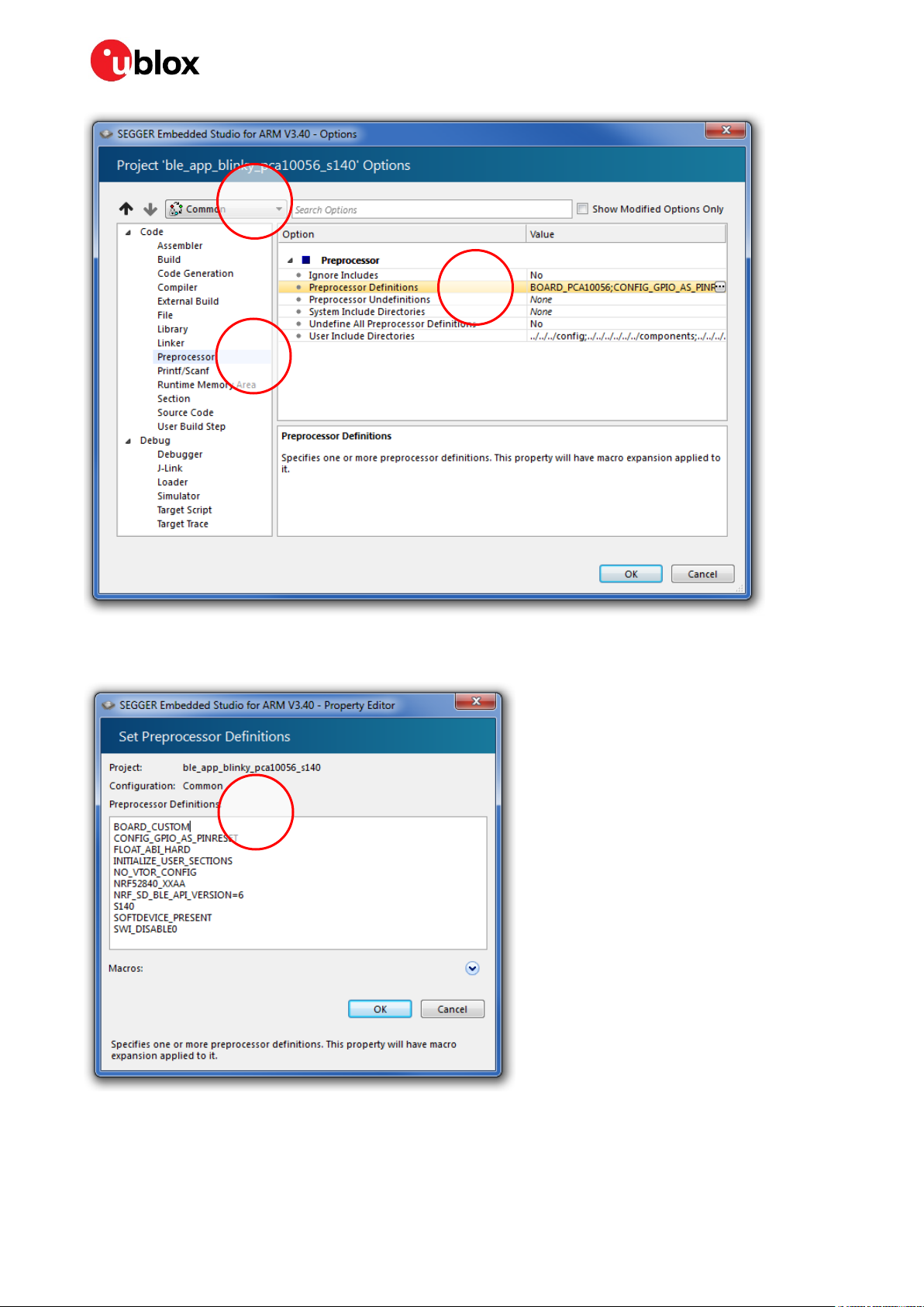
NINA-B3 series - System integration manual
3.
5.
4.
Figure 6: Screenshot with steps to modify the Define statement in SEGGER Embedded Studio
6. Modify the “BOARD_” definition to define the BOARD_CUSTOM
6.
Figure 7: Screenshot with steps to modify the Define statement in SEGGER Embedded Studio
UBX-17056748 - R11 Software Page 21 of 67
C1-Public
Page 22

NINA-B3 series - System integration manual
LF clock source configuration
For more information regarding how to configure your application in the Nordic SDK to use the internal
RC oscillator or an external LFXO please see reference [15].
2.2.2 Bluetooth MAC address and other production data
The open CPU (B30x) variants of the NINA-B3 modules is provided with a Bluetooth MAC address
programmed similar to that in the u-connectXpress variant. If required, this address can be used by
the customer application.
The MAC address is programmed in the CUSTOMER[0] and CUSTOMER[1] registers in the UICR of
the nRF52840 chip. The address can be read and written for example, using Segger J-Link utilities or
the nrfjprog utility from Nordic.
$ nrfjprog.exe --memrd 0x10001080 --n 8
The memory area can be saved and, if the flash is erased, written back later using the savebin and
loadbin utilities in the Segger J-link tool suite.
The UICR memory area also holds the serial number and other information that can be valuable to
save. If you want to save the whole memory area use the following commands:
$ nrfjprog.exe --readuicr uicr.hex
...
$ nrfjprog.exe --program uicr.hex
For additional information and instructions on saving and using the public Bluetooth device address,
see reference [14].
2.3 Flashing the NINA-B31 u-blox software
It is possible to reflash the NINA-B31 module using the UART interface whenever a new version of the
u-connectXpress software is available.
2.3.1 UART flashing
The u-connectXpress software for UART flashing contains two separate .bin files. One bin file
contains the application and the other contains the SoftDevice as listed below:
• Application – NINA-B31X-SW-x.y.z-<build>.bin (Example:
• SoftDevice – NINA-S140-SD-a.b.c.bin (Example:
A signature file for each of the above-mentioned files is also included, as well as a .json header file.
NINA-S140-SD-6.1.1.bin)
Software flashing using s-center
⚠ Flashing of u-blox software requires s-center software version 4.6.2 or later.
NINA-B31X-SW-3.0.0-005.bin)
To flash the module using s-center,
1. Select Tools > Software Update
UBX-17056748 - R11 Software Page 22 of 67
C1-Public
as shown in the following screenshot:
Page 23
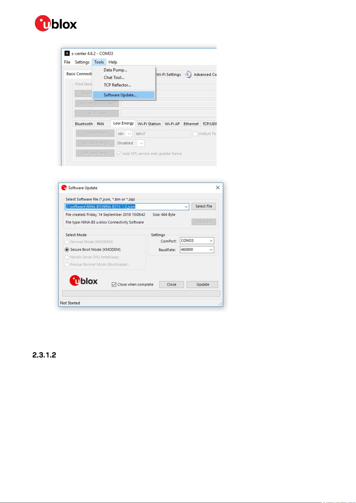
NINA-B3 series - System integration manual
2. Select the .json file.
3. Secure Boot Mode will be set automatically, ensure that the correct COM port is selected then
click the Update button to start the process.
4. The module will then reboot into the bootloader and the flashing of the SoftDevice and the
application will start.
Software flashing using AT command
The flashing functionality in the NINA-B31x module can manage two signed binary images. Image0 is
the application. Image1 is the SoftDevice. The SoftDevice is updated using dual banked approach.
Hence a SoftDevice update will invalidate the application currently flashed in the module, so it is
required to flash the application after a SoftDevice update.
Use the
AT+UFWUPD=<mode>,<baud_rate>[,<id>,<size>,<signature>,<name>,<flags>]
AT+UFWUPD AT command to update the software.
The file download uses an XMODEM protocol. The UART hardware flow is not used during the software
update. See the u-connect AT commands manual [3] for information about the firmware update
command.
☞ The XMODEM protocol uses standard XMODEM-CRC16 protocol and 128 bytes packets.
UBX-17056748 - R11 Software Page 23 of 67
C1-Public
Page 24

NINA-B3 series - System integration manual
2.3.1.2.1 Sample commands executed while flashing the application only
1. Run the AT+UFWUPD command to trigger the u-connectXpress software to accept an application bin
file for download. The application size can be found in the
should be entered in decimal notation. The signature for the application is available in the
NINA-B31X-SI-x.x.x-xxx.txt file.
NINA-B31X-CF-x.x.json file; the size
2. When a ‘C’ character is received from the module, XMODEM download is ready to begin from the
host.
3. Send the application bin file using XMODEM protocol.
4. After a successful file transfer, the module will automatically start the application.
2.3.1.2.2 Sample commands executed when flashing the SoftDevice and application
1. Start the bootloader mode using either:
The AT command Press the SW1 and SW2 buttons during a module reset
2. The “
s <imageid> <signature>” command stores the SoftDevice signature. The image id of the
SoftDevice is 1. The signature is available in the
AT+UFWUPD=1,115200
NINA-S140-SI-x.x.x.txt file.
UBX-17056748 - R11 Software Page 24 of 67
C1-Public
Page 25

NINA-B3 series - System integration manual
3. The “x <imageaddress> <imagesize> <imagename> <permissions> <imageid>” command triggers
the bootloader to accept a file transfer using XMODEM protocol. The image address and image
size can be found in the NINA-B31X-CF-X.Y.json file. Set permission to read/write, rw.
4. When a “
C” character is received from the module, the XMODEM download is ready to begin from
the host.
5. After a successful download of the SoftDevice image, the application image must be flashed.
6. The application is flashed like the SoftDevice. Use image address and image size for the
application image, which can be found in the
NINA-B31X-CF-x.x.json under the label – u-connect.
The image id of the application is 0. The application’s signature is available in the NINA-B31X-SIx.x.x-xxx.txt file. Set permission to read/write/execute, rwx.
7. Store the application image (image id 0) as the startup image with the “
UBX-17056748 - R11 Software Page 25 of 67
C1-Public
f <imageid>” command.
Page 26

NINA-B3 series - System integration manual
8. Reset the module to start up the module with the newly flashed software.
2.4 Flashing the NINA-B30 open CPU software
The NINA-B30 open CPU module can be flashed with the SWD interface.
2.4.1 SWD flashing
For SWD flashing, an external debugger has to be connected to the SWD interface of the
NINA-B30 module. Then an external tool such as the J-flash or the nRF Connect Programmer from
Nordic Semiconductor.
☞ The external debugger SEGGER J-Link BASE works with the NINA-B30 modules.
☞ The EVK-NINA-B30 evaluation kit incorporates an onboard debugger and can therefore be flashed
without any external debugger.
Flashing the software
⚠ Flashing the software will erase the Bluetooth device address, which must be manually rewritten
to the module after flashing. Ensure that you make a note of your Bluetooth device address before
continuing with the flashing procedure. See section 2.2.2 for additional information.
In the nRF Connect Programmer, drag and drop the hex files you want to program into the GUI as
shown in the following screenshot:
UBX-17056748 - R11 Software Page 26 of 67
C1-Public
Page 27

NINA-B3 series - System integration manual
UBX-17056748 - R11 Software Page 27 of 67
C1-Public
Page 28

NINA-B3 series - System integration manual
3 Design-in
3.1 Overview
For an optimal integration of NINA-B3 series modules in the final application board, it is recommended
to follow the design guidelines stated in this chapter. Every application circuit must be properly
designed to guarantee the correct functionality of the related interface, although a number of points
require special attention during the design of the application device.
The following list provides some important points sorted by rank of criticality in the application
design, starting from the highest relevance:
1. Module antenna connection: Ant pad.
The antenna circuit affects the RF compliance of the device integrating the NINA-B3 modules with
the applicable certification schemes. Follow the recommendations provided in section 3.2 for
schematic and layout design.
2. Module supply: VCC, VCC_IO, and GND pins.
The supply circuit affects the performance of the device integrating the NINA-B3 series module.
Follow the recommendations provided in section 3.3.3.2 for schematic and layout design.
3. Analog signals: GPIO
Analog signals are sensitive to noise and should be routed away from high frequency signals.
4. High speed interfaces: UART, SPI and SWD pins.
High speed interfaces can be a source of radiated noise and can affect compliance with regulatory
standards for radiated emissions. Follow the recommendations provided in sections 3.5.1 and 3.3.3.2
for schematic and layout design.
5. System functions: RESET_N, I2C, GPIO and other System input and output pins.
Accurate design is required to guarantee that the voltage level is well defined during module boot.
6. Other pins:
Accurate design is required to guarantee proper functionality.
3.2 Design for NINA family
The NINA-B3 is based on the Nordic nRF52840 chip that has larger dimensions when compared to
the nRF52832 that is used in NINA-B1. Because of this and to enable more GPIO pins underneath the
module, the size of the NINA-B3 series needs to be increased. For instance, the module size of the
NINA B3x2 is 10 x 15.0 mm as compared to the NINA-B112, which is 10 x 14.0 mm.
Pinouts for both the NINA-B1 and W1 are supported so that all modules in the NINA series can be
placed interchangeably on each other’s footprints. However, to accommodate the larger dimension of
the NINA-B3, a keep-out area of 1 mm should be reserved during design. Otherwise the mechanical
design of the NINA-B3 is identical to the NINA-B1 and W1 modules.
3.3 Antenna interface
As the unit cannot be mounted arbitrarily, the placement should be chosen with consideration so that
it does not interfere with radio communications. The NINA-B3x2 with an internal surface mounted
antenna cannot be mounted inside a metal enclosure. No metal casing or plastics using metal flakes
should be used. Avoid metallic based paint or lacquer as well. The NINA-B3x1 offers more freedom, as
an external antenna can be mounted further away from the module.
UBX-17056748 - R11 Design-in Page 28 of 67
C1-Public
Page 29

NINA-B3 series - System integration manual
⚠ According to FCC regulations, the transmission line from the module’s antenna pin to the antenna
or antenna connector on the host PCB is considered part of the approved antenna design.
Therefore, module integrators must either follow exactly one of the antenna reference designs
used in the module’s FCC type approval or certify their own designs.
3.3.1 RF transmission line design (NINA-B3x1 only)
RF transmission lines, such as the ones from the ANT pad up to the related antenna connector or up
to the related internal antenna pad, must be designed so that the characteristic impedance is as close
as possible to 50 Ω. Figure 8 illustrates the design options and the main parameters to be taken into
account when implementing a transmission line on a PCB:
• The micro strip (a track coupled to a single ground plane, separated by dielectric material).
• The coplanar micro strip (a track coupled to ground plane and side conductors, separated by
dielectric materials).
• The strip line (a track sandwiched between two parallel ground planes, separated by dielectric
materials).
Figure 8: Transmission line trace design
To properly design a 50 Ω transmission line, the following remarks should be taken into account:
• The designer should provide enough clearance from surrounding traces and ground in the same
layer; in general, a trace to ground clearance of at least two times the trace width should be
considered and the transmission line should be ‘guarded’ by ground plane area on each side.
• The characteristic impedance can be calculated as a first iteration by using tools provided by the
layout software. It is advisable to ask the PCB manufacturer to provide the final values that are
usually calculated using dedicated software and available stack-ups from production. It could also
be possible to request an impedance coupon on the panel’s side in order to measure the real
impedance of the traces.
• FR-4 dielectric material, although its high losses at high frequencies can be considered in RF
designs providing that:
UBX-17056748 - R11 Design-in Page 29 of 67
C1-Public
Page 30

NINA-B3 series - System integration manual
o RF trace length must be minimized to reduce dielectric losses.
o If traces longer than a few centimeters are needed, it is recommended to use a coaxial
connector and cable to reduce losses.
o Stack-up should allow for thick 50 Ω traces and at least 200 µm of trace width is recommended
to ensure good impedance control over the PCB manufacturing process.
o FR-4 material exhibits poor thickness stability and thus less control of impedance over the
trace length. Contact the PCB manufacturer for specific tolerance of controlled impedance
traces.
• The transmission lines width and spacing to GND must be uniform and routed as smoothly as
possible: route RF lines in 45° angle or in arcs.
• Add GND stitching vias around transmission lines.
• Ensure solid metal connection of the adjacent metal layer on the PCB stack-up to the main ground
layer, providing enough vias on the adjacent metal layer.
• Route RF transmission lines far from any noise source (as switching supplies and digital lines) and
from any sensitive circuit to avoid crosstalk between RF traces and Hi-impedance or analog
signals.
• Avoid stubs on the transmission lines; any component on the transmission line should be placed
with the connected pad over the trace. Also avoid any unnecessary component on RF traces.
Figure 9: Example of RF trace and ground plane design from NINA-B3 Evaluation Kit (EVK)
3.3.2 Antenna design (NINA-B3x1 only)
NINA-B301 and NINA-B311 is suitable for designs where an external antenna is needed due to
mechanical integration or placement of the module.
Designers must take care of the antennas from all perspectives at the beginning of the design phase
when the physical dimensions of the application board are under analysis/decision, because the RF
compliance of the device integrating the NINA-B3 module with all the applicable required certification
schemes heavily depends on the radiating performance of the antennas. The designer is encouraged
to consider one of the u-blox suggested antenna part numbers and follow the layout requirements.
• External antennas, such as a linear monopole:
UBX-17056748 - R11 Design-in Page 30 of 67
C1-Public
Page 31

NINA-B3 series - System integration manual
o External antennas basically do not impose any physical restrictions on the design of the PCB
where the module is mounted.
o The radiation performance mainly depends on the antennas. It is required to select antennas
with optimal radiating performance in the operating bands.
o RF cables should be carefully selected with minimum insertion losses. Additional insertion loss
will be introduced by low quality or long cables. Large insertion loss reduces radiation
performance.
o A high quality 50 Ω coaxial connector provides proper PCB-to-RF-cable transition.
• Integrated antennas such as patch-like antennas:
o Internal integrated antennas impose physical restrictions on the PCB design:
An integrated antenna excites RF currents on its counterpoise, typically the PCB ground plane
of the device that becomes part of the antenna; its dimension defines the minimum frequency
that can be radiated. Therefore, the ground plane can be reduced down to a minimum size that
should be similar to the quarter of the wavelength of the minimum frequency that needs to be
radiated, given that the orientation of the ground plane related to the antenna element must
be considered.
The RF isolation between antennas in the system must be as high as possible and the
correlation between the 3D radiation patterns of the two antennas must be as low as possible.
In general, an RF separation of at least a quarter wavelength between the two antennas is
required to achieve a maximum isolation and low pattern correlation; increased separation
should be considered if possible to maximize the performance and fulfill the requirements in
Table 8.
As a numerical example, the physical restriction to the PCB design can be considered as shown
below:
Frequency = 2.4 GHz Wavelength = 12.5 cm Quarter wavelength = 3.125 cm
1
o Radiation performance depends on the entire product and antenna system design, including
product mechanical design and usage. Antennas should be selected with optimal radiating
performance in the operating bands according to the mechanical specifications of the PCB and
the entire product.
Table 8 summarizes the requirements for the antenna RF interface.
Item Requirements Remarks
Impedance
Frequency
Range
Return Loss S11 < -10 dB (VSWR < 2:1)
Efficiency > -1.5 dB ( > 70% )
Maximum Gain +3 dBi Higher gain antennas could be used, but must be evaluated and/or certified.
Table 8: Summary of antenna interface (ANT) requirements for NINA-B3
50 Ω nominal characteristic
impedance
2400 - 2500 MHz Bluetooth low energy.
recommended
< -6 dB (VSWR < 3:1)
S
11
acceptable
recommended
> -3.0 dB ( > 50% )
acceptable
The impedance of the antenna RF connection must match the 50 Ω
impedance of the ANT pin.
The Return loss or the S
power, measuring how well the primary antenna RF connection matches the
50 Ω characteristic impedance of the ANT pin.
The impedance of the antenna termination must match as much as possible
the 50 Ω nominal impedance of the ANT pin over the operating frequency
range, thus maximizing the amount of the power transferred to the antenna.
The radiation efficiency is the ratio of the radiated power to the power
delivered to the antenna input; the efficiency is a measure of how well an
antenna receives or transmits.
See Section 0 for more information on regulatory requirements.
, as the VSWR, refers to the amount of reflected
11
1
Wavelength referred to a signal propagating over the air
UBX-17056748 - R11 Design-in Page 31 of 67
C1-Public
Page 32

NINA-B3 series - System integration manual
While selecting external or internal antennas, the following recommendations should be observed:
• Select antennas that provide optimal return loss (or VSWR) figure over all the operating
frequencies.
• Select antennas that provide optimal efficiency figure over all the operating frequencies.
• Select antennas that provide an appropriate gain figure (that is, combined antenna directivity and
efficiency figure), so that the electromagnetic field radiation intensity does not exceed the
regulatory limits specified in some countries (for example, by the FCC in the United States).
RF Connector Design
If an external antenna is required, the designer should consider using a proper RF connector. It is the
responsibility of the designer to verify the compatibility between plugs and receptacles used in the
design.
Table 9 suggests some RF connector plugs that can be used by the designers to connect RF coaxial
cables based on the declaration of the respective manufacturers. The Hirose U.FL-R-SMT RF
receptacles (or similar parts) require a suitable mated RF plug from the same connector series. Due
to wide usage of this connector, several manufacturers offer compatible equivalents.
Manufacturer Series Remarks
Hirose U.FL® Ultra Small Surface Mount Coaxial Connector Recommended
I-PEX MHF® Micro Coaxial Connector
Tyco UMCC® Ultra-Miniature Coax Connector
Amphenol RF AMC® Amphenol Micro Coaxial
Lighthorse Technologies, Inc. IPX ultra micro-miniature RF connector
Table 9: U.FL compatible plug connector
Typically, the RF plug is available as a cable assembly. Different types of cable assembly are available;
the user should select the cable assembly best suited to the application. The key characteristics are:
• RF plug type: select U.FL or equivalent
• Nominal impedance: 50 Ω
• Cable thickness: Typically from 0.8 mm to 1.37 mm. Select thicker cables to minimize insertion
loss.
• Cable length: Standard length is typically 100 mm or 200 mm; custom lengths may be available
on request. Select shorter cables to minimize insertion loss.
• RF connector on the other side of the cable: for example another U.FL (for board-to-board
connection) or SMA (for panel mounting)
Consider that SMT connectors are typically rated for a limited number of insertion cycles. In addition,
the RF coaxial cable may be relatively fragile compared to other types of cables. To increase
application ruggedness, connect the U.FL connector to a more robust connector such as SMA fixed
on panel.
☞ A de-facto standard for SMA connectors implies the usage of reverse polarity connectors (RP-
SMA) on Wi-Fi and Bluetooth end products to increase the difficulty for the end user to replace the
antenna with higher gain versions and exceed the regulatory limits.
The following recommendations apply for proper layout of the connector:
• Strictly follow the connector manufacturer’s recommended layout:
UBX-17056748 - R11 Design-in Page 32 of 67
C1-Public
Page 33

NINA-B3 series - System integration manual
o SMA Pin-Through-Hole connectors require GND keep-out (that is, clearance, a void area) on all
the layers around the central pin up to annular pads of the four GND posts.
o UFL surface mounted connectors require no conductive traces (that is, clearance, a void area)
in the area below the connector between the GND land pads.
• If the connector’s RF pad size is wider than the micro strip, remove the GND layer beneath the RF
connector to minimize the stray capacitance thus keeping the RF line 50 Ω. For example, the active
pad of the UF.L connector must have a GND keep-out (that is, clearance, a void area), at least on
the first inner layer to reduce parasitic capacitance to ground.
Integrated antenna design
If integrated antennas are used, the transmission line is terminated by the integrated antennas
themselves. The following guidelines should be followed:
• The antenna design process should begin at the start of the whole product design process. Self-
made PCBs and antenna assembly are useful in estimating overall efficiency and the radiation
path of the intended design.
• Use antennas designed by an antenna manufacturer providing the best possible return loss (or
VSWR).
• Provide a ground plane large enough according to the related integrated antenna requirements.
The ground plane of the application PCB may be reduced down to a minimum size that must be
similar to one quarter of wavelength of the minimum frequency that needs to be radiated,
although overall antenna efficiency may benefit from larger ground planes.
• Proper placement of the antenna and its surroundings is also critical for antenna performance.
Avoid placing the antenna close to conductive or RF-absorbing parts such as metal objects, ferrite
sheets and so on as they may absorb part of the radiated power or shift the resonant frequency of
the antenna or affect the antenna radiation pattern.
• It is highly recommended to strictly follow the detailed and specific guidelines provided by the
antenna manufacturer regarding correct installation and deployment of the antenna system,
including the PCB layout and matching circuitry.
• Further to the custom PCB and product restrictions, antennas may require tuning/matching to
comply with all the applicable required certification schemes. It is recommended to consult the
antenna manufacturer for the design-in guidelines and plan the validation activities on the final
prototypes like tuning/matching and performance measures (see Table 8).
• The RF section may be affected by noise sources like hi-speed digital buses. Avoid placing the
antenna close to buses such as DDR or consider taking specific countermeasures like metal
shields or ferrite sheets to reduce the interference.
⚠ Take care of interaction between co-located RF systems like LTE sidebands on 2.4 GHz band.
Transmitted power may interact or disturb the performance of NINA-B3 modules.
3.3.3 On-board antenna
If a plastic enclosure is used, it is possible to use NINA-B3 with the embedded antenna. In order to
reach an optimum operating performance, follow the instructions provided in the sections below.
NINA-B3x2
• The module shall be placed in the corner of the host PCB with the antennas feed point in the corner
(pin 15 and 16), as shown in Figure 10. Other edge placements positions, with the antenna closest
to the edge, are also possible. These will however give moderate reduced antenna performance
compared to the corner placement.
• A large ground plane on the host PCB is a prerequisite for good antenna performance.
• The host PCB shall include a full GND plane underneath the entire module, including the antenna
section. This to facilitate efficient grounding of the module.
• High / large parts including metal shall not be placed closer than 10 mm to the module’s antenna.
UBX-17056748 - R11 Design-in Page 33 of 67
C1-Public
Page 34

NINA-B3 series - System integration manual
• At least 5 mm clearance between the antenna and the casing is needed. If the clearance is less
than 5 mm, the antenna performance will be affected. PC and ABS gives less impact and POS type
plastic gives more.
• The module shall be placed such that the antenna faces outwards from the product and is not
obstructed by any external items in close vicinity of the products intended use case.
Figure 10: NINA-B3x2 with internal antenna
⚠ Take care when handling the NINA-B3x2. Applying force to the NINA-B3x2 module might damage
the internal antenna.
⚠ Make sure that the end product design is done in such a way that the antenna is not subject to
physical force.
NINA-B3x6 – PCB trace antenna
• The module shall be placed in the center of an edge of the host PCB.
• A large ground plane on the host PCB is a prerequisite for good antenna performance. It is
recommended to have the ground plane extending at least 10 mm on both sides of the module.
See Figure 11.
• The host PCB shall include a full GND plane underneath the entire module, with a ground cut out
under the antenna according to the description in Figure 12.
• The NINA-B3x6 has 4 extra GND pads under the antenna that need to be connected for a good
antenna performance. Detailed measurements of the footprint including this extra GND pads can
be found in the NINA-B3 series Data Sheet [2].
• High / large parts including metal shall not be placed closer than 10 mm to the module’s antenna.
• At least 10 mm clearance between the antenna and the casing is needed. If the clearance is less
than 10 mm, the antenna performance will be affected. PC and ABS gives less impact and POS
type plastic gives more.
• The module shall be placed such that the antenna faces outwards from the product and is not
obstructed by any external items in close vicinity of the products intended use case.
UBX-17056748 - R11 Design-in Page 34 of 67
C1-Public
Page 35

NINA-B3 series - System integration manual
8m
3,1mm
Figure 11: Extend GND plane outside the NINA-B3x6 module
Figure 12: Size of the GND cut out for the NINA-B3x6 module
3.4 Supply interfaces
3.4.1 Module supply design
A good connection of the module’s VCC pin with DC supply source is required for correct RF
performance. The guidelines are summarized below:
• The VCC connection must be as wide and short as possible.
• The VCC connection must be routed through a PCB area separated from sensitive analog signals
and sensitive functional units. It is a good practice to interpose at least one layer of PCB ground
between the VCC track and other signal routing.
UBX-17056748 - R11 Design-in Page 35 of 67
C1-Public
Page 36

NINA-B3 series - System integration manual
There is no strict requirement for adding bypass capacitance to the supply net close to the module.
But depending on the layout of the supply net and other consumers on the same net, bypass
capacitors might still be beneficial. Though the GND pins are internally connected, connect all the
available pins to solid ground on the application board, as a good (low impedance) connection to an
external ground can minimize power loss and improve RF and thermal performance.
3.5 Serial interfaces
3.5.1 Asynchronous serial interface (UART) design
The layout of the UART bus should be made so that noise injection and cross talk are avoided.
It is recommended to use the hardware flow control with RTS/CTS to prevent temporary UART buffer
overrun.
The flow control signals RTS/CTS are active low thus a 0 (ON state =low level) will allow the UART to
transmit.
• CTS is an input to the NINA-B3 module and if the host applies a 0 (ON state = low level), then the
module is allowed to transmit.
• RTS is an output off the NINA-B3 module and the module will apply a 0 (ON state = low level) when
it is ready to receive transmission.
3.5.2 Serial peripheral interface (SPI)
The layout of the SPI bus should be made so that noise injection and cross talk are avoided.
3.5.3 I2C interface
The layout of the I2C bus should be made so that noise injection and cross talk are avoided.
3.5.4 QSPI interface
The layout of the QSPI bus should be made so that noise injection and cross talk are avoided.
3.5.5 USB interface
The layout of the USB bus should be made so that noise injection and cross talk are avoided.
3.6 NFC interface
⚠ The pins for the NFC interface can also be used as normal GPIOs. In NINA-B30 series modules,
ensure that the NFC pins are configured correctly in software. Connecting an NFC antenna to the
pins configured as GPIO will damage the module. In NINA-B31 series modules, the NFC pins will
always be set to "NFC mode".
The NFC antenna coil must be connected differentially between the NFC1 and NFC2 pins of the
device.
Two external capacitors should be used to tune the resonance of the antenna circuit to 13.56 MHz.
The required tuning capacitor value is given by the below equations: an antenna inductance of L
2 μH will give tuning capacitors in the range of 130 pF on each pin. For good performance, match the
total capacitance on NFC1 and NFC2.
The NINA-B3 modules have been tested with a 3x3 cm PCB trace antenna, so it is recommended to
keep an antenna design close to these measurements. You can still use a smaller or larger antenna as
long as it is tuned to resonate at 13.56 MHz. To comply with European regulatory demands, the NFC
UBX-17056748 - R11 Design-in Page 36 of 67
C1-Public
ANT
=
Page 37

NINA-B3 series - System integration manual
antenna must be placed in such a way that the space between the NINA-B3 module and the remote
NFC transmitter is always within 3 meters during transmission.
Figure 13: NFC antenna design
=
(
2 × 13.56
1
)
1
=
× +
2
+
=
(
2 × 13.56
2
)
3.6.1 Battery protection
If the antenna is exposed to a strong NFC field, current may flow in the opposite direction on the
supply because of parasitic diodes and ESD structures.
If the battery used does not tolerate a return current, a series diode must be placed between the
battery and the device in order to protect the battery.
3.7 General High Speed layout guidelines
These general design guidelines are considered as best practices and are valid for any bus present in
the NINA-B3 series modules; the designer should prioritize the layout of higher speed buses. Low
frequency signals are generally not critical for layout.
⚠ One exception is represented by High Impedance traces (such as signals driven by weak pull
resistors) that may be affected by crosstalk. For those traces, a supplementary isolation of 4w
from other buses is recommended.
3.7.1 General considerations for schematic design and PCB floor-planning
• Verify which signal bus requires termination and add series resistor terminations to the
schematics.
• Carefully consider the placement of the module with respect to antenna position and host
processor.
• Verify with PCB manufacturer allowable stack-ups and controlled impedance dimensioning.
• Verify that the power supply design and power sequence are compliant with NINA-B3 series
module specification (refer to section 1.4).
UBX-17056748 - R11 Design-in Page 37 of 67
C1-Public
Page 38

NINA-B3 series - System integration manual
3.7.2 Module placement
• Accessory parts like bypass capacitors should be placed as close as possible to the module to
improve filtering capability, prioritizing the placement of the smallest size capacitor close to
module pads.
⚠ Particular care should be taken not to place components close to the antenna area. The designer
should carefully follow the recommendations from the antenna manufacturer about the distance
of the antenna vs. other parts of the system. The designer should also maximize the distance of
the antenna to Hi-frequency buses like DDRs and related components or consider an optional
metal shield to reduce interferences that could be picked up by the antenna thus reducing the
module’s sensitivity.
• An optimized module placement allows better RF performance. See Antenna interfaces section
for more information on antenna consideration during module placement.
3.7.3 Layout and manufacturing
• Avoid stubs on high speed signals. Even through-hole vias may have an impact on signal quality.
• Verify the recommended maximum signal skew for differential pairs and length matching of
buses.
• Minimize the routing length; longer traces will degrade signal performance. Ensure that the
maximum allowable length for high speed buses is not exceeded.
• Ensure that you track your impedance matched traces. Consult with your PCB manufacturer early
in the project for proper stack-up definition.
• RF and digital sections should be clearly separated on the board.
• Ground splitting is not allowed below the module.
• Minimize the bus length to reduce potential EMI issues from digital buses.
• All traces (including low speed or DC traces) must couple with a reference plane (GND or power);
Hi-speed buses should be referenced to the ground plane. In this case, if the designer needs to
change the ground reference, an adequate number of GND vias must be added in the area of
transition to provide a low impedance path between the two GND layers for the return current.
• Hi-Speed buses are not allowed to change reference plane. If a reference plane change is
unavoidable, some capacitors should be added in the area to provide a low impedance return path
through the different reference planes.
• Trace routing should keep a distance greater than 3w from the ground plane routing edge.
• Power planes should keep a distance from the PCB edge sufficient to route a ground ring around
the PCB, and the ground ring must then be connected to other layers through vias.
3.8 Module footprint and paste mask
The mechanical outline of the NINA-B3 series module can be found in the NINA-B3 series Data Sheet
[2]. The proposed land pattern layout reflects the pad’s layout of the module.
The Non Solder Mask Defined (NSMD) pad type is recommended over the Solder Mask Defined (SMD)
pad type, which implements the solder mask opening 50 μm larger per side than the corresponding
copper pad.
The suggested paste mask layout for the NINA-B3 series modules is to follow the copper mask layout
as described in the NINA-B3 series Data Sheet [2].
⚠ These are recommendations only and not specifications. The exact mask geometries, distances,
and stencil thicknesses must be adapted to the specific production processes of the customer.
UBX-17056748 - R11 Design-in Page 38 of 67
C1-Public
Page 39

NINA-B3 series - System integration manual
3.9 Thermal guidelines
The NINA-B3 series modules have been successfully tested from -40 °C to +85 °C. The NINA-B3 series
module is a low power device and will generate only a small amount of heat during operation. A good
grounding should still be observed for temperature relief during high ambient temperatures.
3.10 ESD guidelines
The immunity of devices integrating NINA-B3 modules to Electrostatic Discharge (ESD) is part of the
Electromagnetic Compatibility (EMC) conformity, which is required for products bearing the CE
marking, compliant with the R&TTE Directive (99/5/EC), the EMC Directive (89/336/EEC) and the Low
Voltage Directive (73/23/EEC) issued by the Commission of the European Community.
Compliance with these directives implies conformity to the following European Norms for device ESD
immunity: ESD testing standard
EN 301 489-1
in Table 10.
,
ETSI EN 301 489-7, ETSI EN 301 489-24
CENELEC EN 61000-4-2
, the requirements of which are summarized
and the radio equipment standards
ETSI
The ESD immunity test is performed at the enclosure port, defined by
physical boundary through which the electromagnetic field radiates. If the device implements an
integral antenna, the enclosure port is seen as all insulating and conductive surfaces housing the
device. If the device implements a removable antenna, the antenna port can be separated from the
enclosure port. The antenna port includes the antenna element and its interconnecting cable
surfaces.
The applicability of ESD immunity test to the whole device depends on the device classification as
defined by
the related interconnecting cables to auxiliary equipment depends on device accessible interfaces
and manufacturer requirements, as defined by
Contact discharges are performed at conductive surfaces, while air discharges are performed at
insulating surfaces. Indirect contact discharges are performed on the measurement setup horizontal
and vertical coupling planes as defined in
ETSI EN 301 489-1
. Applicability of the ESD immunity test to the related device ports or
ETSI EN 301 489-1
CENELEC EN 61000-4-2
.
.
ETSI EN 301 489-1
as the
☞ For the definition of integral antenna, removable antenna, antenna port, and the device
classification, refer to the
to
CENELEC EN 61000-4-2
Application Category Immunity Level
All exposed surfaces of the radio equipment and ancillary
equipment in a representative configuration
Table 10: Electromagnetic Compatibility ESD immunity requirements as defined by CENELEC EN 61000-4-2, ETSI EN 301
489-1, ETSI EN 301 489-7, ETSI EN 301 489-24
ETSI EN 301 489-1
.
. For the contact and air discharges definitions, refer
Indirect Contact Discharge ±8 kV
NINA-B3 is manufactured taking into account specific standards to minimize the occurrence of ESD
events; the highly automated process complies with IEC61340-5-1 (STM5.2-1999 Class M1 devices)
standard, and therefore the designer should implement proper measures to protect any pin that may
be exposed to the end user from ESD events.
Compliance with the standard protection level specified in EN61000-4-2 can be achieved by including
ESD protections in parallel to the line, close to areas accessible by the end user.
UBX-17056748 - R11 Design-in Page 39 of 67
C1-Public
Page 40

NINA-B3 series - System integration manual
•
when handling the PCB must always be
Before mounting an antenna patch,
•
develop charges (e.g. patch antenna ~10
•
the RF input, do not touch any exposed
an exposed antenna area is touched in a
proper ESD protection measures in the
•
antennas to the receiver’s RF pin, make
4 Handling and soldering
☞ No natural rubbers, hygroscopic materials or materials containing asbestos are employed.
4.1 Packaging, shipping, storage and moisture preconditioning
For information pertaining to reels, tapes or trays, moisture sensitivity levels (MSL), shipment and
storage, as well as drying for preconditioning, refer to the NINA-B3 series Data Sheet [2] and u-blox
package information guide [1].
4.2 Handling
The NINA-B3 series modules are Electrostatic Discharge (ESD) sensitive devices and require special
precautions during handling. Particular care must be exercised when handling patch antennas, due to
the risk of electrostatic charges. In addition to standard ESD safety practices, the following measures
should be taken into account whenever handling the receiver:
Unless there is a galvanic coupling between
the local GND (i.e. the work table) and the
PCB GND, then the first point of contact
between the local GND and PCB GND.
•
connect the ground of the device
When handling the RF pin, do not come into
contact with any charged capacitors and be
careful when contacting materials that can
pF, coax cable ~50-80 pF/m, soldering iron,
…)
To prevent electrostatic discharge through
antenna area. If there is any risk that such
non-ESD protected work area, implement
design.
When soldering RF connectors and patch
sure to use an ESD safe soldering iron (tip).
4.3 Soldering
4.3.1 Reflow soldering process
The NINA-B3 series modules are surface mount modules supplied on a FR4-type PCB with
gold-plated connection pads and produced in a lead-free process with a lead-free soldering paste. The
bow and twist of the PCB is maximum 0.75% according to IPC-A-610E. The thickness of solder resist
between the host PCB top side and the bottom side of the NINA-B3 series module must be considered
for the soldering process.
UBX-17056748 - R11 Handling and soldering Page 40 of 67
C1-Public
Page 41

NINA-B3 series - System integration manual
The module is compatible with the industrial reflow profile for RoHS solders. Use of "No Clean"
soldering paste is strongly recommended.
The reflow profile used is dependent on the thermal mass of the entire populated PCB, heat transfer
efficiency of the oven and particular type of solder paste used. The optimal soldering profile used must
be trimmed for each case depending on the specific process and PCB layout.
Process parameter Unit Target
Pre-heat Ramp up rate to T
T
T
tS (from +25 °C) s 150
tS (Pre-heat) s 60 to 120
Peak TL °C 217
tL (time above TL) s 40 to 60
TP (absolute max) °C 245
Cooling Ramp-down from TL K/s 4
Allowed soldering cycles - 1
°C 150
SMIN
°C 200
SMAX
K/s 3
SMIN
Table 11: Recommended reflow profile
Figure 14: Reflow profile
☞ Lower value of T
and slower ramp down rate (2 – 3 °C/sec) is preferred.
P
☞ After reflow soldering, optical inspection of the modules is recommended to verify proper
alignment.
⚠ Target values in Table 11 should be taken as general guidelines for a Pb-free process. Refer to the
JEDEC J-STD-020C [4] standard for further information.
4.3.2 Cleaning
Cleaning the modules is not recommended. Residues underneath the modules cannot be easily
removed with a washing process.
• Cleaning with water will lead to capillary effects where water is absorbed in the gap between the
baseboard and the module. The combination of residues of soldering flux and encapsulated water
leads to short circuits or resistor-like interconnections between neighboring pads. Water will also
damage the sticker and the ink-jet printed text.
UBX-17056748 - R11 Handling and soldering Page 41 of 67
C1-Public
Page 42

NINA-B3 series - System integration manual
• Cleaning with alcohol or other organic solvents can result in soldering flux residues flooding into
the two housings, areas that are not accessible for post-wash inspections. The solvent will also
damage the sticker and the ink-jet printed text.
• Ultrasonic cleaning will permanently damage the module, in particular the crystal oscillators.
For best results, use a "no clean" soldering paste and eliminate the cleaning step after the soldering
process.
4.3.3 Other remarks
• Only a single reflow soldering process is allowed for boards with a module populated on them.
• Boards with combined through-hole technology (THT) components and surface-mount
technology (SMT) devices may require wave soldering to solder the THT components. Only a single
wave soldering process is allowed for boards populated with the modules. The Miniature Wave
Selective Solder process is preferred over the traditional wave soldering process.
• Hand soldering is not recommended.
• Rework is not recommended.
• Conformal coating may affect the performance of the module, so it is important to prevent the
liquid from flowing into the module. The RF shields do not provide protection for the module from
coating liquids with low viscosity, and so care is required in applying the coating. Conformal
coating of the module will void the warranty.
• Grounding metal covers: attempts to improve grounding by soldering ground cables, wick or other
forms of metal strips directly onto the EMI covers is made at the customer's own risk and will void
the module’s warranty. The numerous ground pins are adequate to provide optimal immunity to
interferences.
• The module contains components that are sensitive to ultrasonic waves. Use of any ultrasonic
processes such as cleaning, welding etc., may damage the module. Use of ultrasonic processes on
an end product integrating this module will void the warranty.
UBX-17056748 - R11 Handling and soldering Page 42 of 67
C1-Public
Page 43

NINA-B3 series - System integration manual
5 Regulatory information and requirements
The NINA-B3 series modules are certified for use in different regions and countries such as Europe,
USA and Canada. See the NINA-B3 series Data Sheet [2] for a list of approved countries/regions where
NINA-B3 modules are approved for use. Each market has its own regulatory requirements that must
be fulfilled, and the NINA-B3 series modules comply with the requirements for a radio transmitter in
each of the listed markets.
In some cases, limitations must be placed on the end product that integrates a
NINA-B3 module to comply with the regulatory requirements. This section lists the limitations and
requirements that a module integrator must take into consideration. This section is divided into
different subsections for each market. A checklist is included at the end of this section to summarize
some of the requirements for each market.
⚠ This section reflects u-blox’ interpretation of different regulatory requirements of a radio device
in each country/region. It does not cover all the requirements placed on an end product that uses
the radio module of u-blox or any other manufacturer.
5.1 ETSI – European market
5.1.1 Compliance statement
Detailed information about European Union regulatory compliance for the NINA-B3 series modules is
available in the NINA-B3 Declaration of Conformity [12].
⚠ Module integrators are required to make their own “Declaration of Conformity”, in which test
standards and directives that are tested and fulfilled by the end product are listed.
5.1.2 NINA-B3 Software security considerations
⚠ An end user cannot be allowed to change the software on the NINA-B3 module to any unauthorized
software, or modify the existing software in an unauthorized way. A module integrator must
consider this in the end product design. Typically, the SWD interface (the SWDCLK and SWDIO
pins) must not be accessible by the end user.
5.1.3 Output power limitation
The Radio Equipment Directive requires radio transmitters that have an Equivalent Isotropically
Radiated Power (EIRP) of 10 dBm or more, to either implement an adaptivity feature or reduce its
medium utilization.
The NINA-B3 series modules are based on the Nordic Semiconductor nRF52840 chip, which supports
multiple radio protocols such as Bluetooth low energy, IEEE 802.15.4 with thread etc.
Since Bluetooth low energy does not support either adaptivity or reduced medium utilization, a
NINA-B3 Bluetooth LE implementation on the European market must have an EIRP of less than 10
dBm.
⚠ In the European market, it is the end product manufacturer that holds the responsibility that
these limitations are followed. If the u-blox module integrator is not the end product manufacturer,
the module integrator should make sure that this information is shared with the end product
manufacturer.
☞ Radio protocols based on 802.15.4, which supports adaptivity is allowed an EIRP of 10 dBm or
higher.
UBX-17056748 - R11 Regulatory information and requirements Page 43 of 67
C1-Public
Page 44

NINA-B3 series - System integration manual
EIRP is calculated as:
EIRP(dBm) = P
where P
is the output power of the transmitter, L is the path loss of the transmission line between
TX
the transmitter and antenna, and G
(dBm) – L(dB) + GTX(dBi)
TX
is the maximum gain of the transmit antenna. Consider the
TX
following for each of these components:
• Output power:
o The output power setting of the NINA-B3 module. An end product user must not be able to
increase the setting above the 10 dBm EIRP limit, by sending configuration commands etc.
o The operating temperature of the end product. The output power of a transmitter is typically
increased as the ambient temperature is lowered. The operating temperature range of NINAB3 is -40 to +85 °C, and across this range the output power can typically vary by 1 dB. The
output power at the lowest operating temperature (yielding the highest output power) must
be considered for the EIRP calculation.
• Path loss – Long antenna cables or PCB traces, RF switches, etc. will attenuate the power reaching
the antenna. This path loss should be measured and taken into consideration for the EIRP
calculation.
• Antenna gain - The maximum gain of the transmit antenna must be considered for the EIRP
calculation.
Implementation in the NINA-B31 series
In the u-connectXpress software, output power can be configured by using the Bluetooth
configuration AT command.
AT+UBTCFG=4,<output power>
The default output power setting is ‘6’, which typically corresponds to +6 dBm output power at room
temperature. This setting is based on the following assumptions:
• -40 °C is the lowest operating temperature of the end product
• The path loss is negligible
• The maximum antenna gain of the end-product antenna is +3 dBi.
With these assumptions, the EIRP will be just below the 10 dBm limit. If, for instance the antenna gain
is instead +2 dBi and an antenna cable with 1 dB path loss is used, a higher output power setting could
be used.
☞ The maximum output power setting, ‘8’, typically corresponds to +8 dBm output power, though
the output power setting does not match the actual output power 1:1. Use a power meter or
spectrum analyzer to measure the actual output power before committing to a power setting.
Implementation in the NINA-B30 series
An integrator of the open CPU variant of the NINA-B3 series on the European market must make sure
that an end user cannot in any way configure the output power of the radio to 10 dBm EIRP or above.
5.1.4 Safety Compliance
⚠ In order to fulfill the EN 60950-1 safety standard, the NINA-B3 series modules must be supplied
with a Class-2 Limited Power Source.
UBX-17056748 - R11 Regulatory information and requirements Page 44 of 67
C1-Public
Page 45

NINA-B3 series - System integration manual
5.2 FCC/ISED – US/Canadian markets
5.2.1 Compliance statements
The NINA-B3 series modules comply with Part 15 of the FCC Rules and with Industry Canada licenseexempt RSS standard(s). Operation is subject to the following two conditions:
1. This device may not cause harmful interference, and
2. This device must accept any interference received, including interference that may cause
undesired operation.
This equipment has been tested and found to comply with the limits for a Class B digital device,
pursuant to Part 15 of the FCC Rules. These limits are designed to provide reasonable protection
against harmful interference in a residential installation. This equipment generates, uses and can
radiate radio frequency energy and, if not installed and used in accordance with the instructions, may
cause harmful interference to radio communications. However, there is no guarantee that the
interference will not occur in a particular installation. If this equipment does cause harmful
interference to radio or television reception, which can be determined by turning the equipment off
and on, the user is encouraged to correct the interference using either one or more of the following
measures:
• Reorient or relocate the receiving antenna
• Increase the separation between the equipment and receiver
• Connect the equipment into an outlet on a circuit different from that to which the receiver is
connected.
• Consult the dealer or an experienced radio/TV technician for help.
⚠ Since u-blox cannot control how integrators of NINA-B30 will operate the module, an extra
precaution is required by the FCC/ISED. Customers of NINA-B30 will be required to undergo a
’Change in ID’ process, see Section 5.2.5 for more information.
⚠ The NINA-B3 modules are for OEM integrations only. The end product has to be professionally
installed in such a manner that only the authorized antennas can be used. See Section 5.2.3 for
more information.
⚠ Any changes to hardware, hosts or co-location configuration may require new radiated emission
and SAR evaluation and/or testing. Any changes or modifications NOT explicitly APPROVED by ublox may cause the NINA-B3 module to cease to comply with the FCC rules part 15 thus void the
user’s authority to operate the equipment on the US market.
Model FCC ID ISED Certification Number
NINA-B301 XPYNINAB30 8595A-NINAB30
NINA-B302 XPYNINAB30 8595A-NINAB30
NINA-B306 XPYNINAB30 8595A-NINAB30
NINA-B311 XPYNINAB31 8595A-NINAB31
NINA-B312 XPYNINAB31 8595A-NINAB31
NINA-B316 XPYNINAB31 8595A-NINAB31
Table 12: FCC IDs and ISED Certification Numbers for the NINA-B3 series modules
5.2.2 RF Exposure
The NINA-B3 series modules comply with the FCC radiation exposure limits and the requirements of
IC RSS-102 issue 5 radiation exposure limits set forth for an uncontrolled environment.
UBX-17056748 - R11 Regulatory information and requirements Page 45 of 67
C1-Public
Page 46

NINA-B3 series - System integration manual
☞ Having a separation distance of minimum 10 mm between the user and/or bystander and the
antenna and /or radiating element ensures that the maximum output power of NINA-B3 is below
the SAR test exclusion limits presented in KDB 447498 D01v06 (US market limits).
☞ Having a separation distance of minimum 15 mm between the user and/or bystander and the
antenna and /or radiating element ensures that the output power (e.i.r.p.) of NINA-B3 is below the
SAR evaluation Exemption limits defined in RSS-102 issue 5 (Canadian market limits).
5.2.3 Antenna selection
⚠ For NINA-B301 and NINA-B311, an external antenna connector (U.FL. connector) reference design
is available (Appendix B.1) and must be followed to comply with the NINA-B30/NINA-B31 FCC/IC
modular approval. Use only those antennas that have been authorized for use with NINA-B3; see
Section 5.10 for a list of pre-approved antennas.
☞ u-blox has provided these pre-approved antennas and reference design to enable quick time to
market, but it is possible and encouraged for customers to add their own antennas and connector
designs. These must be approved by u-blox and in some cases tested. Contact your nearest u-blox
support for more information about this process.
5.2.4 IEEE 802.15.4 channel map limitation
The 2.4 GHz band used by 802.15.4 communications is segmented into 16 channels, ranging from
channel 11 at 2405 MHz to channel 26 at 2480 MHz, with 5 MHz channel spacing. Due to the wide
spectral properties of the 802.15.4 signal, the use of channel 26 results in too much power being
transmitted in the FCC restricted band starting at 2483.5 MHz. As a result, channel 26 must not be
used on the US/Canadian market.
Implementation in NINA-B31 series
IEEE 802.15.4 is currently not supported in the u-connect software. No additional effort is needed.
Implementation in NINA-B30 series
Integrators of the open CPU variant of the NINA-B3 series will have to make a “change in FCC ID” filing
to inherit the test results of the u-blox FCC compliance tests. In this filing process it must be made
clear that the software application has been limited to not use channel 26, and that it cannot be
‘unlocked’ by an end user. It should not be possible for an end user to change the software on the
module to any unauthorized or modified software that allows the use of 802.15.4 channel 26.
Typically, the SWD interface on the NINA-B30 module, which allows full access to all registers and
code space, must be made unavailable to end users.
5.2.5 Change in ID/Multiple Listing process
☞ A Change in ID can be done only for the NINA-B30 series.
The open CPU feature of the NINA-B30 series allows customers to create their own software
applications using the NINA-B3 hardware. This software will have full control of radio parameters, and
it is possible to configure the radio in a way that it will be non-compliant with the FCC regulatory
requirements.
For any product including an FCC/ISED approved radio device, it will be the sole responsibility of the
FCC/ISED ID holder, in this case u-blox, to ensure that the product complies with the FCC radio
regulations. Since the software applications created by integrators of the NINA-B30 series cannot be
controlled by u-blox, the module integrator will have to take over this responsibility. This process is
known as a ‘change in ID’ in the US and ‘multiple listing’ in Canada.
UBX-17056748 - R11 Regulatory information and requirements Page 46 of 67
C1-Public
Page 47

NINA-B3 series - System integration manual
Most FCC accredited test houses can provide the service to make a change in ID. Module integrators
can also make an application themselves to a Telecommunication Certification Body (TCB). Typically,
the following documentation has to be submitted:
• A permission letter, signed by u-blox, that allows the module integrator (or test house) to make
the change in ID.
• An application letter stating that there is no change in the design, circuitry, or construction of the
NINA-B30 module, and that the original NINA-B30 test results are still representative of the new
product. Minor cosmetic differences are allowed but must be described.
• Photos of the product showing the nameplate or label containing the new FCC ID.
• The user manual for the product.
• (Optional) Short- and long-term confidentiality requests. The FCC typically makes all submitted
photos and documentation publically available on their website. Applicants can request that
certain sensitive information is published later or not at all.
5.2.6 End product verification requirements
⚠ The modular transmitter approval of NINA-B3, or any other radio module, does not exempt the end
product from being evaluated against applicable regulatory demands.
The evaluation of the end product shall be performed with the NINA-B3 module installed and
operating in a way that reflects the intended end product use case. The upper frequency
measurement range of the end product evaluation is the 5th harmonic of 2.4 GHz as declared in 47
CFR Part 15.33 (b)(1).
The following requirements apply to all products that integrate a radio module:
• Subpart B - UNINTENTIONAL RADIATORS
To verify that the composite device of host and module comply with the requirements of FCC part
15B, the integrator shall perform sufficient measurements using ANSI 63.4-2014.
• Subpart C - INTENTIONAL RADIATORS
It is required that the integrator carries out sufficient verification measurements using ANSI
63.10-2013 to validate that the fundamental and out of band emissions of the transmitter part of
the composite device complies with the requirements of FCC part 15C.
When the items listed above are fulfilled, the end product manufacturer can use the authorization
procedures as mentioned in Table 1 of 47 CFR Part 15.101, before marketing the end product. This
means the customer has to either market the end product under a Suppliers Declaration of
Conformity (SDoC) or to certify the product using an accredited test lab.
5.2.7 End product labelling requirements
US market
An end product using the NINA-B3 series modules must have a label containing, at least, the
information shown in Figure 15 or Figure 16. The label must be affixed on an exterior surface of the
end product such that it will be visible upon inspection in compliance with the modular approval
guidelines developed by the FCC. In accordance with 47 CFR § 15.19, the end product shall bear the
following statement in a conspicuous location on the device:
“This device complies with Part 15 of the FCC Rules. Operation is subject to the following two
conditions:
1. This device may not cause harmful interference, and
2. This device must accept any interference received, including interference that may cause
undesired operation.”
UBX-17056748 - R11 Regulatory information and requirements Page 47 of 67
C1-Public
Page 48

NINA-B3 series - System integration manual
☞ When the device is so small or for such use that it is not practicable to place the statement above
on it, the information shall be placed in a prominent location in the instruction manual or pamphlet
supplied to the user or, alternatively, shall be placed on the container in which the device is
marketed.
In case, where the final product will be installed in locations where the end user is unable to see the
FCC ID and/or this statement, the FCC ID and the statement shall also be included in the end product
manual.
Canadian market
The host product shall be properly labelled to identify the modules within the host product.
The Innovation, Science and Economic Development Canada certification label of a module shall be
clearly visible at all times when installed in the host product; otherwise, the host product must be
labelled to display the Innovation, Science and Economic Development Canada certification number
for the module, preceded by the word “Contains” or similar wording expressing the same meaning, as
shown in Figure 15 or Figure 16.
Le produit hôte devra être correctement étiqueté, de façon à permettre l’identification des modules
qui s’y trouvent.
L’étiquette d’homologation d’un module d’Innovation, Sciences et Développement économique
Canada devra être posée sur le produit hôte à un endroit bien en vue, en tout temps. En l’absence
d’étiquette, le produit hôte doit porter une étiquette sur laquelle figure le numéro d’homologation du
module d’Innovation, Sciences et Développement économique Canada, précédé du mot « contient »,
ou d’une formulation similaire allant dans le même sens et qui va comme suit:
This device contains
FCC ID: XPYNINAB30
IC: 8595A-NINAB30
Figure 15: Example of an end product label that includes a NINA-B30 series module
This device contains
FCC ID: XPYNINAB31
IC: 8595A-NINAB31
Figure 16: Example of an end product label that includes a NINA-B31 series module
5.2.8 End product user manual requirements
US market
As stated in Section 5.2.7.1, labelling requirements for the US market, the following statement shall
be placed in a prominent section of the instruction manual, when it cannot feasibly be placed on the
physical device:
“This device complies with Part 15 of the FCC Rules. Operation is subject to the following two
conditions:
1. This device may not cause harmful interference, and
2. This device must accept any interference received, including interference that may cause
undesired operation.”
The statement “this device contains” along with the FCC ID of NINA-B30 or NINA-B31, as shown in
Figure 15 or Figure 16 shall also be placed in the instruction manual when it cannot be placed on the
physical device.
UBX-17056748 - R11 Regulatory information and requirements Page 48 of 67
C1-Public
Page 49

NINA-B3 series - System integration manual
Canadian market
User manuals for license-exempt radio apparatus shall contain the following text, or an equivalent
notice that shall be displayed in a conspicuous location, either in the user manual or on the device, or
both:
“This device complies with Part 15 of the FCC Rules. Operation is subject to the following two
conditions:
1. This device may not cause harmful interference, and
2. This device must accept any interference received, including interference that may cause
undesired operation.”
Under Industry Canada regulations, this radio transmitter can only operate using an antenna of a type
and maximum (or lesser) gain approved for the transmitter by Industry Canada. To reduce potential
radio interference to other users, the antenna type and its gain should be chosen in such a way that
the equivalent isotropically radiated power (e.i.r.p.) is not more than that is necessary for successful
communication.
Le manuel d’utilisation des appareils radio exempts de licence doit contenir l’énoncé qui suit, ou
l’équivalent, à un endroit bien en vue dans le manuel d’utilisation ou sur l’appareil, ou encore aux deux
endroits.
“Le présent appareil est conforme aux CNR d’Industrie Canada applicables aux appareils radio
exempts de licence. L’exploitation est autorisée aux deux conditions suivantes:
1. l’appareil ne doit pas produire de brouillage;
2. l’utilisateur de l’appareil doit accepter tout brouillage radioélectrique subi, même si le brouillage
est susceptible d’en compromettre le fonctionnement.”
Conformément aux réglementations d’Industry Canada, cet émetteur radio ne peut fonctionner qu’à
l’aide d’une antenne dont le type et le gain maximal (ou minimal) ont été approuvés pour cet émetteur
par Industry Canada. Pour réduire le 25ecess d’interférences avec d’autres utilisateurs, il faut choisir
le type d’antenne et son gain de telle sorte que la puissance isotrope rayonnée équivalente (p.i.r.e) ne
soit pas supérieure à celle requise pour obtenir une communication satisfaisante.
5.3 MIC - Japanese market
5.3.1 Compliance statement
The NINA-B3 series modules comply with the Japanese Technical Regulation Conformity
Certification of Specified Radio Equipment (ordinance of MPT N°. 37, 1981), Article 2, Paragraph 1:
• Item 19 "2.4 GHz band wide band low power data communication system".
5.3.2 48-bit address requirement
Radio devices on the Japanese market, which can be connected directly or indirectly to a public
network, must have an at least 48-bit (12 hex) long ID code. In practice this means that the device
addresses used in the radio communication protocol (Bluetooth, Thread, ZigBee, Gazell etc.) must be
at least 48 bits.
☞ Note that this requirement is not applicable to devices only intended for use in private or personal
networks.
UBX-17056748 - R11 Regulatory information and requirements Page 49 of 67
C1-Public
Page 50
NINA-B3 series - System integration manual
Implementation in the NINA-B30 series
The requirements on a NINA-B30 design depend on the used radio protocol(s):
• The Bluetooth protocol uses 48-bit addressing, no additional effort is needed.
• IEEE 802.15.4 based protocols, such as Thread and ZigBee, use (at the MAC layer) a combination
of 16- and 64-bit addresses. The 16-bit (‘short’) address can be used to reduce overhead in
communications. However, each device must have a 64-bit (‘extended’) address, and can always
be accessed using this address. Because of this no additional effort is needed when using an
802.15.4 based protocol.
• Protocols based on the 2.4 GHz proprietary mode do not necessarily follow any standards, so there
is no guarantee that the 48-bit addressing requirement will be fulfilled. If the end product can be
connected to, or accessed through, a public network using a proprietary protocol, it is the end
product manufacturer’s responsibility to make sure that the protocol uses at least 48-bit
addressing.
⚠ Failure to comply with these requirements will void the NINA-B3 Japan certification, and it will be
illegal to place the end product on the Japanese market.
Implementation in the NINA-B31 series
All the radio communication protocols supported in the NINA-B31 series use at least 48 bit long
addressing. No further actions are required by the module integrator.
5.3.3 End product labelling requirement
When a product integrating a NINA-B3 series module is placed on the Japanese market the product
must be affixed with a label with the “Giteki” marking as shown in Figure 17. The marking must be
visible for inspection.
204-810006
Figure 17: Giteki mark, R and the NINA-B3 MIC certification number
☞ The required minimum size of the Giteki mark is Ø3.0 mm.
5.3.4 End product user manual requirement
As the MIC ID is not included on the NINA-B3 series label, the end product manufacturer must include
a copy of the NINA-B3 Japan Radio Certificate to the end product technical documentation.
☞ Contact the u-blox support team in your area to obtain a copy of the NINA-B3 Japan Radio
Certificate (see the Contact
5.4 NCC – Taiwanese market
5.4.1 Compliance statements
• 經型式認證合格之低功率射頻電機,非經許可,公司、商號或使用者均不得擅自變更頻率、 加大功率或變
更原設計之特性及功能。
• 低功率射頻電機之使用不得影響飛航安全及干擾合法通信;經發現有干擾現象時,應立即停用,並改善至
無干擾時方得繼續使用。前項合法通信,指依電信法規定作業之無線電通信。低功率射頻電機須忍受合法
通信或工業、科學及醫療用電波輻射性電機設備之干擾。
UBX-17056748 - R11 Regulatory information and requirements Page 50 of 67
C1-Public
Page 51

NINA-B3 series - System integration manual
Contains Transmitter Module
含發射器模組
Contains Transmitter Module
含發射器模組
Contains Transmitter Module
含發射器模組
Contains Transmitter Module
含發射器模組
Statement translation:
• Without permission granted by the NCC, any company, enterprise, or user is not allowed to change
frequency, enhance transmitting power or alter original characteristic as well as performance to
an approved low power radio-frequency devices.
• The low power radio-frequency devices shall not influence aircraft security and interfere legal
communications; If found, the user shall cease operating immediately until no interference is
achieved. The said legal communications means radio communications is operated in compliance
with the Telecommunications Act. The low power radio-frequency devices must be susceptible
with the interference from legal communications or ISM radio wave radiated devices.
5.4.2 End product labelling requirement
When a product integrating a NINA-B3 series module is placed on the Taiwanese market, the product
must be affixed with a label or marking containing at least the following information:
NINA-B301 Label
內
Figure 18: Example of an end product label that includes a NINA-B301 module
:
CCAI18LP1970T4
NINA-B302 Label
內
Figure 19: Example of an end product label that includes a NINA-B302 module
:
CCAI18LP197AT6
NINA-B306 Label
內
Figure 20: Example of an end product label that includes a NINA-B306 module
:
CCAI19LP1670T0
NINA-B311 Label
內
Figure 21: Example of an end product label that includes a NINA-B311 module
UBX-17056748 - R11 Regulatory information and requirements Page 51 of 67
C1-Public
:
CCAI18LP197BT8
Page 52

NINA-B3 series - System integration manual
Contains Transmitter Module
含發射器模組
Contains Transmitter Module
含發射器模組
NINA-B312 Label
內
Figure 22: Example of an end product label that includes a NINA-B312 module
:
CCAI18LP197CT0
NINA-B316 Label
內
Figure 23: Example of an end product label that includes a NINA-B316 module
Any similar wording that expresses the same meaning may be used. The marking must be visible for
inspection.
:
CCAI19LP1680T3
☞ Note that each NINA-B3 module variant has its own certification number.
Module variant NCC ID
NINA-B301 CCAI18LP1970T4
NINA-B302 CCAI18LP197AT6
NINA-B306 CCAI19LP1670T0
NINA-B311 CCAI18LP197BT8
NINA-B312 CCAI18LP197CT0
NINA-B316 CCAI19LP1680T3
Table 13: NINA-B3 series NCC ID certification numbers
5.5 KCC – South Korean market
5.5.1 Compliance statement
The NINA-B3 series modules are certified by the Korea Communications Commission (KCC).
5.5.2 End product labeling requirements
When a product containing a NINA-B3 series module is placed on the South Korean market, the
product must be affixed with a label or marking containing the KCC logo and certification number as
shown in the following figures:
R-C-ULX-NINA-B30
Figure 24: Sample label of an end product that includes a NINA-B30 series module
UBX-17056748 - R11 Regulatory information and requirements Page 52 of 67
C1-Public
Page 53

NINA-B3 series - System integration manual
R-C-ULX-NINA-B31
Figure 25: Sample label of an end product that includes a NINA-B31 series module
5.5.3 End product user manual requirements
The KCC logo and NINA-B3 certification numbers shown in section 5.5.2 must also be included in the
end products user manual.
5.6 Anatel Brazil compliance
When a product containing a NINA-B3 module is placed on the Brazilian market, the product must be
affixed with a label or marking containing the Anatel logo, NINA-B3 Homologation number:
03851-19-05903 and a statement claiming that the device may not cause harmful interference but
must accept it (Resolution No 506).
03851-19-05903
“Este equipamento opera em caráter secundário, isto é, não
tem direito a proteção contra interferência prejudicial, mesmo
de estações do mesmo tipo, e não pode causar interferência a
sistemas operando em caráter primário.”
Statement translation:
“This equipment operates on a secondary basis and, consequently, must accept harmful interference,
including from stations of the same kind, and may not cause harmful interference to systems
operating on a primary basis.”
When the device is so small or for such use that it is not practicable to place the statement above on
it, the information shall be placed in a prominent location in the instruction manual or pamphlet
supplied to the user or, alternatively, shall be placed on the container in which the device is marketed.
In case, where the final product will be installed in locations where the end-user is not able to see the
Anatel logo, NINA-B3 Homologation number and/or this statement, the Anatel logo, NINA-B3
Homologation number and the statement shall also be included in the end-product manual.
5.7 Australia and New Zealand regulatory compliance
The NINA-B3 modules are compliant with AS/NZS 4268:2012/AMDT 1:2013 standard
– Radio equipment and systems – Short range devices – Limits and methods of
standard measurement made by the Australian Communications and Media Authority
(ACMA).
The NINA-B3 module test reports can be used as part of evidence in obtaining permission the
Regulatory Compliance Mark (RCM). To meet overall Australian and/or New Zealand compliance on
the end product, the integrator must create a compliance folder containing all the relevant
compliance test reports.
UBX-17056748 - R11 Regulatory information and requirements Page 53 of 67
C1-Public
Page 54

NINA-B3 series - System integration manual
APPROVED
TA-2019/1202
More information on registration as a Responsible Integrator and labeling requirements will be found
at the following websites:
Australian Communications and Media Authority web site http://www.acma.gov.au/.
New Zealand Radio Spectrum Management Group web site www.rsm.govt.nz.
5.8 South Africa regulatory compliance
The NINA-B3 modules are compliant and certified by the Independent Communications Authority of
South Africa (ICASA). End products that are made available for sale or lease or is supplied in any other
manner in South Africa shall have a legible label permanently affixed to its exterior surface. The label
shall have the ICASA logo and the ICASA issued license number as shown in the figure below. The
minimum width and height of the ICASA logo shall be 3 mm. The approval labels must be purchased
by the customer’s local representative directly from the approval authority ICASA. A sample of a
NINA-B3 ICASA label is included below:
More information on registration as a Responsible Integrator and labeling requirements will be found
at the following website:
Independent Communications Authority of South Africa (ICASA) web site - https://www.icasa.org.za
5.9 Integration checklist
The following checklist can be used to get an overview of the requirements of each market. It is in no
way a complete list of all actions required, but should cover the essentials of integrating a NINA-B3
radio module.
General requirements
The SWD interface cannot be accessed by an end product user.
Specific to the European market
The E.I.R.P of the end product is measured to be within the applicable limit.
A Class-2 limited power source is used to supply the module.
A Declaration of Conformity has been created.
Specific to the US and Canadian markets
(NINA-B30) A Change in ID/Multiple Listing has been performed.
(NINA-B3x1) The antenna connector reference design has been followed and a pre-approved
antenna is used with the end product. If not, then u-blox has been contacted to get approval to
make changes and/or add a new antenna.
(NINA-B30) If 802.15.4 is used, the radio channel 26 has been disabled and end product users’
cannot enable it.
The fundamental and out of band emissions of the end product has been measured and complies
with the applicable limits.
An SDoC has been created, or an accredited test lab has been used to certify the end product.
The end product labelling requirements are fulfilled.
UBX-17056748 - R11 Regulatory information and requirements Page 54 of 67
C1-Public
Page 55

NINA-B3 series - System integration manual
The end product documentation requirements are fulfilled. The necessary legal statements are
included at a prominent location in the user guide.
Specific to the Japanese market
(NINA-B30) If applicable, the product fulfills the 48-bit addressing requirements.
The end product labelling requirements are fulfilled.
A copy of the NINA-B3 Japan Radio Certificate has been included in the end product technical
documentation
Specific to the Taiwanese market
The end product labelling requirements are fulfilled.
Specific to the South Korean market
The end product labelling requirements are fulfilled.
The end product user manual requirements are fulfilled.
Specific to the Brazilian market
The end product labelling requirements are fulfilled.
The end product user manual requirements are fulfilled.
Specific to the Australian and/or New Zealand markets
The end product labelling requirements are fulfilled.
A compliance folder containing all the relevant compliance test reports is created and available.
Specific to the South African market
The end product labelling requirements are fulfilled.
5.10 Pre-approved antennas list
This section lists the different external antennas that are pre-approved for use together with the
NINA-B3 series modules.
☞ Note that not all antennas are approved for use in all markets/regions.
UBX-17056748 - R11 Regulatory information and requirements Page 55 of 67
C1-Public
Page 56

NINA-B3 series - System integration manual
for
5.10.1 Antenna accessories
Name U.FL to SMA adapter cable
Connector U.FL and SMA jack (outer thread and pin receptacle)
Impedance 50 Ω
Minimum cable loss 0.5 dB, The cable loss must be above the minimum cable loss to
meet the regulatory requirements. Minimum cable length 100 mm.
Comment The SMA connector can be mounted in a panel. See Appendix B.1
information how to integrate the U.FL connector.
Approval RED, MIC, NCC, KCC, ANATEL, ACMA and ICASA
Name U.FL to Reverse Polarity SMA adapter cable
Connector U.FL and Reverse Polarity SMA jack (outer thread and pin)
Impedance 50 Ω
Minimum cable loss 0.5 dB, The cable loss must be above the minimum cable loss to
meet the regulatory requirements. Minimum cable length 100 mm.
Comment The Reverse Polarity SMA connector can be mounted in a panel. See
Appendix B.1 for information how to integrate the U.FL connector.
It is required to followed this reference design to comply with the
NINA-W1 FCC/IC modular approvals.
Approval FCC, IC, RED, MIC, NCC, KCC, ANATEL, ACMA and ICASA
5.10.2 Single band antennas
NINA-B302 and NINA-B312 (u-blox LILY antenna)
Manufacturer ProAnt
Gain +3 dBi
Impedance N/A
Size (HxWxL) 3.0 x 3.8 x 9.9 mm
Type PIFA
Comment SMD PIFA antenna on NINA-B302 and NINA-B312. Should not be mounted
inside a metal enclosure.
Approval FCC, IC, RED, MIC, NCC, KCC, ANATEL, ACMA and ICASA
NINA-B306 and NINA-B316
Manufacturer ProAnt
Gain +3 dBi
Impedance N/A
Size (HxWxL) 1.1 x 3.4 x 10 mm
Type PCB trace
Comment PCB antenna on NINA-B306 and NINA-B316. Should not be mounted inside a
metal enclosure.
Approval FCC, IC, RED, MIC, NCC, KCC, ANATEL, ACMA and ICASA
UBX-17056748 - R11 Regulatory information and requirements Page 56 of 67
C1-Public
Page 57
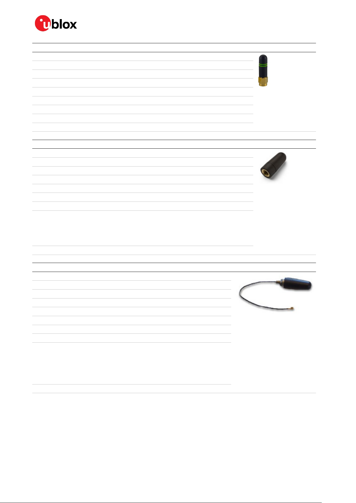
NINA-B3 series - System integration manual
GW.26.0111
Manufacturer Taoglas
Polarization Vertical
Gain +2.0 dBi
Impedance 50 Ω
Size Ø 7.9 x 30.0 mm
Type Monopole
Connector SMA (M) .
Comment To be mounted on the U.FL to SMA adapter cable.
Approval RED, MIC, NCC, KCC, ANATEL, ACMA and ICASA
Ex-IT 2400 RP-SMA 28-001
Manufacturer ProAnt
Polarization Vertical
Gain +3.0 dBi
Impedance 50 Ω
Size Ø 12.0 x 28.0 mm
Type Monopole
Connector Reverse Polarity SMA plug (inner thread and pin receptacle).
Comment This antenna requires to be mounted on a metal ground plane for best
performance.
To be mounted on the U.FL to Reverse Polarity SMA adapter cable.
An SMA version antenna is also available but not recommended for use (Ex-IT
2400 SMA 28-001).
Approval FCC, IC, RED, MIC, NCC, KCC, ANATEL, ACMA and ICASA
Ex-IT 2400 MHF 28-001
Manufacturer ProAnt
Polarization Vertical
Gain +2.0 dBi
Impedance 50 Ω
Size Ø 12.0 x 28.0 mm
Type Monopole
Cable length 100 mm
Connector U.FL. connector
Comment This antenna requires to be mounted on a metal ground plane for
best performance.
To be mounted on a U.FL connector.
See Appendix B.1 for information how to integrate the U.FL
connector. It is required to followed this reference design to comply
with the NINA –B3 FCC/IC modular approvals.
Approval FCC, IC, RED, MIC, NCC, KCC, ANATEL, ACMA and ICASA
UBX-17056748 - R11 Regulatory information and requirements Page 57 of 67
C1-Public
Page 58

NINA-B3 series - System integration manual
SMA version antenna is also available but not recommended for use
Ex-IT 2400 RP-SMA 70-002
Manufacturer ProAnt
Polarization Vertical
Gain +3.0 dBi
Impedance 50 Ω
Size Ø 10 x 83 mm
Type Monopole
Connector Reverse Polarity SMA plug (inner thread and pin receptacle)
Comment To be mounted on the U.FL to Reverse Polarity SMA adapter cable. An
(Ex-IT 2400 SMA 70-002).
Approval FCC, IC, RED, MIC, NCC, KCC, ANATEL, ACMA and ICASA
InSide-2400
Manufacturer ProAnt
Gain +3.0 dBi
Impedance 50 Ω
Size 27 x 12 mm (triangular)
Type Patch
Cable length 100 mm
Connector U.FL. connector
Comment Should be attached to a plastic enclosure or part for best
performance.
To be mounted on a U.FL connector.
See Appendix B.1 for information how to integrate the U.FL
connector. It is required to followed this reference design to comply
with the NINA-W1 FCC/IC modular approvals.
Approval FCC, IC, RED, MIC, NCC, KCC, ANATEL, ACMA and ICASA
FlatWhip-2400 SMA
Manufacturer ProAnt
Gain +3.0 dBi
Impedance 50 Ω
Size Ø 50.0 x 30.0 mm
Type Monopole
Connector SMA plug (inner thread and pin)
Comment To be mounted on the U.FL to SMA adapter cable.
Approval RED, MIC, NCC, KCC, ANATEL, ACMA and ICASA
FlatWhip-2400 RP-SMA
Manufacturer ProAnt
Gain +3.0 dBi
Impedance 50 Ω
Size Ø 50.0 x 30.0 mm
Type Monopole
Connector Reverse Polarity SMA plug (inner thread and pin receptacle).
Comment To be mounted on the U.FL to SMA adapter cable.
Approval FCC, IC, RED, MIC, NCC, KCC, ANATEL, ACMA and ICASA
UBX-17056748 - R11 Regulatory information and requirements Page 58 of 67
C1-Public
Page 59

NINA-B3 series - System integration manual
6 Product testing
6.1 u-blox in-series production test
u-blox focuses on high quality for its products. All units produced are fully tested automatically in the
production line. A stringent quality control process has been implemented in the production line.
Defective units are analyzed in detail to improve the production quality.
This is achieved with automatic test equipment (ATE) in the production line, which logs all production
and measurement data. A detailed test report for each unit can be generated from the system.
Figure 26 illustrates the typical automatic test equipment (ATE) in a production line.
The following tests are performed as part of the production tests:
• Digital self-test (software download, MAC address programming)
• Measurement of voltages and currents
• Functional tests
• Digital I/O tests
• Measurement of RF characteristics in all supported bands (such as receiver RSSI calibration,
frequency tuning of the reference clock, calibration of transmitter power levels and so on.)
Figure 26: Automatic test equipment for module testing
6.2 OEM manufacturer production test
As the testing is already performed by u-blox, an OEM manufacturer does not need to repeat software
tests or measurement of the module’s RF performance or tests over analog and digital interfaces in
their production test.
However, an OEM manufacturer should focus on:
• Module assembly on the device; it should be verified that:
o Soldering and handling processes have not damaged the module components
o All module pins are well soldered on the device board
o There are no short circuits between pins
• Component assembly on the device; it should be verified that:
UBX-17056748 - R11 Product testing Page 59 of 67
C1-Public
Page 60

NINA-B3 series - System integration manual
o Communication with host controller can be established
o The interfaces between the module and device are working
o Overall RF performance test of the device including the antenna
Dedicated tests can be implemented to check the device. For example, the measurement of module
current consumption when set in a specified state can detect a short circuit if compared with a
“Golden Device” result.
The standard operational module firmware and test software on the host can be used to perform
functional tests (communication with the host controller, check interfaces) and to perform basic RF
performance tests.
6.2.1 “Go/No go” tests for integrated devices
A “Go/No go” test compares the signal quality with a “Golden Device” in a location with a known signal
quality. This test can be performed after establishing a connection with an external device.
A very simple test can be performed by just scanning for a known Bluetooth low energy device and
checking the signal level.
☞ These kinds of test may be useful as a “go/no go” test but not for RF performance measurements.
This test is suitable to check the functionality of the communication with the host controller and the
power supply. It is also a means to verify if components are well-soldered.
A basic RF functional test of the device including the antenna can be performed with standard
Bluetooth low energy devices as remote stations. The device containing the NINA-B3 series module
and the antennas should be arranged in a fixed position inside an RF shield box to prevent
interferences from other possible radio devices to obtain stable test results.
UBX-17056748 - R11 Product testing Page 60 of 67
C1-Public
Page 61

NINA-B3 series - System integration manual
Appendix
A Glossary
Abbreviation Definition
ADC Analog to digital converter
ATE Automatic test equipment
BLE Bluetooth low energy
CTS Clear To send
DCX Data/Command signal
DDR Dual-Data rate
EMC Electro Magnetic Compatibility
EMI Electro Magnetic Interference
ESD Electro static discharge
FCC Federal Communications Commission
GATT Generic ATTribute profile
GND Ground
GPIO General Purpose Input/Output
I2C Inter-Integrated Circuit
LDO Low drop out
LED Light-Emitting Diode
LFXO Low Frequency Crystal Oscillator
MAC Media access control
MISO Master input, slave output
MOSI Master output, slave input
MSL Moisture sensitivity level
NFC Near Field Communication
NSMD Non solder mask defined
PCB Printed circuit board
PIFA Planar inverted-F antenna
QDEC Quadrature DECoder
QSPI Quad serial peripheral interface
RF Radio frequency
RoHS Restriction of hazardous substances
RSSI Received signal strength indicator
RTS Request to send
RXD Receive data
SCL Signal clock
SDL Specification and description language
SMA SubMiniature version A
SMD Solder mask defined
SMPS Switching mode power supply
SMT Surface-Mount technology
SPI Serial peripheral interface
SWD Serial wire debug
Thread Networking protocol for Internet of Things (IoT) "smart" home automation devices to communicate on a
UBX-17056748 - R11 Appendix Page 61 of 67
C1-Public
Page 62

NINA-B3 series - System integration manual
Abbreviation Definition
local wireless mesh network
THT Through-Hole Technology
TXD Transmit data
UART Universal asynchronous receiver/transmitter
UICR User information configuration registers
USB Universal serial bus
VCC IC power-supply pin
VSWR Voltage standing wave ratio
Table 14: Explanation of the abbreviations and terms used
B Antenna reference designs
Designers can take full advantage of NINA-B3’s Single-Modular Transmitter certification approval by
integrating the u-blox reference design into their products. This approach requires compliance with
the following rules:
• Only listed antennas can be used. Refer to NINA-B3 series data sheet [2] for the listed antennas.
• Schematics and parts used in the design must be identical to the reference design, please use u-
blox’ validated parts for antenna matching.
• PCB layout must be identical to the one provided by u-blox, please implement one of the reference
designs included in this section or contact u-blox.
• The designer must use the PCB stack-up provided by u-blox. RF traces on the carrier PCB are part
of the certified design.
The available designs are presented in this section.
B.1 Reference design for external antennas (U.FL connector)
When using the NINA-B301/B311 together with this antenna reference design, the circuit trace
layout must be made in strict compliance with the instructions below.
Components connected to the RF trace must be kept as indicated in the reference design. The
reference design uses a U.FL micro coaxial connector to connect the external antenna via a 50 Ω
coaxial cable.
Figure 27: Antenna reference design
UBX-17056748 - R11 Appendix Page 62 of 67
C1-Public
Page 63

NINA-B3 series - System integration manual
B.1.1 Floor plan
This section describes where the critical components and copper traces are positioned on the
reference design.
1
4
5
2
6
3
Figure 28: NINA-B301/B311 antenna reference design
Reference Part Manufacturer Description
1 NINA-B301/B311 u-blox NINA-B3 module with antenna pin
2 U.FL-R-SMT-1(10) Hirose Coaxial connector, 0 – 6 GHz, for external antenna
3 Carrier PCB Should have a solid GND inner layer underneath and around the
RF components (vias and small openings are allowed)
4 RF trace Antenna coplanar microstrip, matched to 50 Ω
5 GND trace Minimum required top layer GND-trace, see Figure 30
6 Copper keep out Keep this area free from any copper on the top layer
Table 15: Included parts in the antenna connector design
B.1.2 RF trace specification
The 50 Ω coplanar micro-strip dimensions used in the reference design are shown in Figure 29 and
Table 16. GND stitching vias should be used around the RF trace to ensure a proper GND connection.
No other components are allowed within this area.
The solid GND layer beneath the ‘top layer’ shall surround at least the entire RF trace and connector.
No signal traces are allowed to be routed on the GND layer within this area but vias and small openings
are allowed.
Figure 29: Coplanar micro-strip dimension specification
UBX-17056748 - R11 Appendix Page 63 of 67
C1-Public
Page 64

NINA-B3 series - System integration manual
Ω as possible)
ε
Reference Item Value
S Spacing 200 +/- 50 μm
W Conductor width 300 +/- 30 μm (match as close to 50
T Copper and plating/surface
coating thickness
H Conductor height 150 +/- 20 μm
r
Table 16: Coplanar micro-strip specification
Dielectric constant
(relative permittivity)
35 +/- 15 μm
3.77 +/- 0.5 @ 2 GHz
☞ The GND spacing requirements of the NINA ANT and U.FL connector RF pins are greater than the
spacing requirement of a 50 Ω coplanar micro-strip. However, at the conductor width and height
specified in Table 16, the increased spacing to GND does not affect the trace impedance
significantly for short trace lengths, and it will still be close to 50 Ω.
Figure 30: RF trace and minimum required GND trace of the U.FL antenna connector reference design. Dimensions are
shown in mm.
UBX-17056748 - R11 Appendix Page 64 of 67
C1-Public
Page 65

NINA-B3 series - System integration manual
Related documents
[1] u-blox package information guide, UBX-14001652
[2] NINA-B3 series data sheet, UBX-17052099
[3] u-connect AT commands manual, UBX-14044127
[4] JEDEC J-STD-020C - Moisture/Reflow Sensitivity Classification for Non Hermetic Solid State
Surface Mount Devices.
[5] IEC EN 61000-4-2 - Electromagnetic compatibility (EMC) - Part 4-2: Testing and measurement
techniques – Electrostatic discharge immunity test
[6] ETSI EN 301 489-1 - Electromagnetic compatibility and Radio spectrum Matters (ERM);
ElectroMagnetic Compatibility (EMC) standard for radio equipment and services; Part 1:
Common technical requirements
[7] IEC61340-5-1 - Protection of electronic devices from electrostatic phenomena – General
requirements
[8] ETSI EN 60950-1:2006 - Information technology equipment – Safety – Part 1: General
requirements
[9] FCC Regulatory Information, Title 47 – Telecommunication
[10] JESD51 – Overview of methodology for thermal testing of single semiconductor devices
[11] Nordic Semiconductor InfoCenter - https://infocenter.nordicsemi.com/index.jsp
[12] NINA-B3 declaration of conformity, UBX-18053818
[13] NINA-B31 getting started, UBX-18022394
[14] Using the public IEEE address from UICR, UBX-19055303
[15] RC oscillator configuration for nRF5 open CPU modules, UBX-20009242
☞ For product change notifications and regular updates of u-blox documentation, register on our
website, www.u-blox.com.
UBX-17056748 - R11 Related documents Page 65 of 67
C1-Public
Page 66

NINA-B3 series - System integration manual
Removed references to application development using Arm Mbed for
). Updated flashing
.
Updated regulatory information section with instructions on how to comply with
). Added information
). Added
to reflect the
B3
variants. Also added regulatory guidelines for the South Korean market. Updated
connectScript version to 1.0.1 and modified the product status for
). Corrected
). Removed nRF Go Studio
Added instructions on how to put an end product on the Brazilian, Australian, New
the chapter
Revision history
Revision Date Name Comments
R01 16-Nov-2017 apet, ajoh,
ajah, kgom
R02 22-Mar-2018 apet
R03 8-Jun-2018 apet, kgom Updated Nordic SDK section to SDKv15 (section 2.2.1
R04 13-Sep-2018 ajoh, kgom Changed the product status to Initial Production. Updated Table 1 and Table 2
R05 14-Feb-2019 ajoh, fbro,
mper
R06 16-Apr-2019 ajoh, fbro Changed the product status to Initial Production. Updated Section 5
Initial release.
NINA-B30x open CPU modules.
instructions in Flashing the NINA-B31 u-blox connectivity software (section 2.3).
regulatory restrictions for different global markets (section 5
about an FCC approved antenna connector reference design in Appendix B.
Added instructions for using s-center to flash NINA-B31 (section 2.3.1.1
instructions on how to put an end product on the Japanese and Taiwanese markets
(section
Added the software version for java script.
Added the new antenna type NINA-B3x6.
change with respect to SWD interface access, which applies for all NINA-
5).
some values in recommended reflow profile (Table 11).
R07 10-May-2019 fbro Updated u-
NINA-B31x-20B to Initial Production.
Included information about Bluetooth MAC address (section 2.2.2
information about UART flow control (section 3.5.1). Updated Single band antennas
(section 5.10.2).
R08 23-Sep-2019 mape Updated some links to Nordic InfoCenter (section 2.2.1.1
and replaced with nRF Connect Programmer (section 2.4.1).
R09 20-Dec-2019 mwej
Zealand and South Africa markets (section 5).
R10 20-Apr-2020 mape Removed all u-connectScript references. Included small correction in
Flashing the NINA-B31 u-blox software
R11 8-Dec-2020 mape Added information about NINA-B306-01B variant.
, section 2.3.1.2.1.
UBX-17056748 - R11 Revision history Page 66 of 67
C1-Public
Page 67

NINA-B3 series - System integration manual
Contact
For complete contact information, visit us at www.u-blox.com.
u-blox Offices
North, Central and South America
u-blox America, Inc.
Phone: +1 703 483 3180
E-mail: info_us@u-blox.com
Regional Office West Coast:
Phone: +1 408 573 3640
E-mail: info_us@u-blox.com
Technical Support:
Phone: +1 703 483 3185
E-mail: support@u-blox.com
Headquarters
Europe, Middle East, Africa
u-blox AG
Phone: +41 44 722 74 44
E-mail: info@u-blox.com
Support: support@u-blox.com
Asia, Australia, Pacific
u-blox Singapore Pte. Ltd.
Phone: +65 6734 3811
E-mail: info_ap@u-blox.com
Support: support_ap@u-blox.com
Regional Office Australia:
Phone: +61 2 8448 2016
E-mail: info_anz@u-blox.com
Support: support_ap@u-blox.com
Regional Office China (Beijing):
Phone: +86 10 68 133 545
E-mail: info_cn@u-blox.com
Support: support_cn@u-blox.com
Regional Office China (Chongqing):
Phone: +86 23 6815 1588
E-mail: info_cn@u-blox.com
Support: support_cn@u-blox.com
Regional Office China (Shanghai):
Phone: +86 21 6090 4832
E-mail: info_cn@u-blox.com
Support: support_cn@u-blox.com
Regional Office China (Shenzhen):
Phone: +86 755 8627 1083
E-mail: info_cn@u-blox.com
Support: support_cn@u-blox.com
Regional Office India:
Phone: +91 80 405 092 00
E-mail: info_in@u-blox.com
Support: support_in@u-blox.com
Regional Office Japan (Osaka):
Phone: +81 6 6941 3660
E-mail:
Support: support_jp@u-blox.com
Regional Office Japan (Tokyo):
Phone: +81 3 5775 3850
E-mail: info_jp@u-blox.com
Support: support_jp@u-blox.com
Regional Office Korea:
Phone: +82 2 542 0861
E-mail: info_kr@u-blox.com
Support: support_kr@u-blox.com
Regional Office Taiwan:
Phone: +886 2 2657 1090
E-mail: info_tw@u-blox.com
Support: support_tw@u-blox.com
info_jp@u-blox.com
UBX-17056748 - R11 Contact Page 67 of 67
C1-Public
 Loading...