

Page 1
NEO-D9S
u-blox D9 correction data receiver
Integration manual
Abstract
This document describes the features and specifications of the u-blox D9
correction data receiver.
www.u-blox.com
UBX-19026111 - R05
C1-Public
Page 2

NEO-D9S-Integration manual
Document information
Title NEO-D9S
Subtitle u-blox D9 correction data receiver
Document type Integration manual
Document number UBX-19026111
Revision and date R05 17-Nov-2020
Document status Early production information
Disclosure restriction C1-Public
This document applies to the following products:
Product name Type number Firmware version PCN reference
NEO-D9S NEO-D9S-00B-00 PMP 1.04 N/A
u-blox reserves all rights to this document and the information contained herein. Products, names, logos and designs
described herein may in whole or in part be subject to intellectual property rights. Reproduction, use, modification or
disclosure to third parties of this document or any part thereof without the express permission of u-blox is strictly prohibited.
The information contained herein is provided "as is" and u-blox assumes no liability for the use of the information. No warranty,
either express or implied, is given with respect to, including but not limited to, the accuracy, correctness, reliability and fitness
for a particular purpose of the information. This document may be revised by u-blox at any time. For most recent documents,
please visit www.u blox.com.
Copyright © 2020, u-blox AG.
u-blox is a registered trademark of u-blox Holding AG in the EU and other countries.
UBX-19026111 - R05
C1-Public Early production information
Page 2 of 51
Page 3

NEO-D9S-Integration manual
Contents
1 Integration manual structure............................................................................................ 5
2 System description...............................................................................................................6
2.1 Overview.................................................................................................................................................... 6
2.1.1 Satellite L band DGNSS................................................................................................................6
2.2 Architecture..............................................................................................................................................6
2.2.1 Block diagram..................................................................................................................................6
3 Receiver functionality..........................................................................................................7
3.1 Receiver configuration........................................................................................................................... 7
3.1.1 Changing the receiver configuration..........................................................................................7
3.1.2 Default L band configuration.......................................................................................................7
3.1.3 Default interface settings............................................................................................................ 7
3.1.4 Basic receiver configuration.........................................................................................................8
3.1.5 L band service selection............................................................................................................... 8
3.1.6 Power management....................................................................................................................... 9
3.2 Communication interfaces................................................................................................................. 10
3.2.1 UART...............................................................................................................................................11
3.2.2 I2C interface..................................................................................................................................12
3.2.3 SPI interface..................................................................................................................................15
3.2.4 USB interface................................................................................................................................16
3.3 Predefined PIOs..................................................................................................................................... 17
3.3.1 D_SEL..............................................................................................................................................17
3.3.2 RESET_N........................................................................................................................................17
3.3.3 SAFEBOOT_N................................................................................................................................17
3.3.4 TX_READY..................................................................................................................................... 18
3.3.5 EXTINT............................................................................................................................................18
3.4 Antenna supervisor..............................................................................................................................18
3.4.1 Antenna voltage control - ANT_OFF........................................................................................20
3.4.2 Antenna short detection - ANT_SHORT_N............................................................................ 20
3.4.3 Antenna short detection auto recovery.................................................................................. 21
3.4.4 Antenna open circuit detection - ANT_DETECT................................................................... 21
3.5 Security................................................................................................................................................... 22
3.5.1 Receiver status monitoring....................................................................................................... 22
3.6 Forcing a receiver reset....................................................................................................................... 22
3.7 Firmware upload....................................................................................................................................22
4 Design..................................................................................................................................... 23
4.1 Pin assigment........................................................................................................................................ 23
4.2 Antenna...................................................................................................................................................24
4.2.1 Antenna bias.................................................................................................................................27
4.3 Power supply.......................................................................................................................................... 29
4.3.1 VCC: Main supply voltage.......................................................................................................... 29
4.3.2 NEO-D9S power supply.............................................................................................................. 29
4.4 NEO-D9S minimal design................................................................................................................... 30
4.5 EOS/ESD precautions.......................................................................................................................... 30
4.5.1 ESD protection measures.......................................................................................................... 31
UBX-19026111 - R05
C1-Public Early production information
Contents Page 3 of 51
Page 4

4.5.2 EOS precautions...........................................................................................................................31
4.5.3 Safety precautions...................................................................................................................... 32
4.6 Electromagnetic interference on I/O lines.......................................................................................32
4.6.1 General notes on interference issues...................................................................................... 32
4.6.2 In-band interference mitigation................................................................................................ 33
4.6.3 Out-of-band interference........................................................................................................... 33
4.7 Layout...................................................................................................................................................... 34
4.7.1 Placement......................................................................................................................................34
4.7.2 Thermal management................................................................................................................ 34
4.7.3 Package footprint, copper and paste mask........................................................................... 34
4.7.4 Layout guidance........................................................................................................................... 36
4.8 Design guidance....................................................................................................................................38
4.8.1 General considerations............................................................................................................... 38
4.8.2 RF front-end circuit options...................................................................................................... 38
4.8.3 Antenna/RF input........................................................................................................................ 39
4.8.4 Schematic design........................................................................................................................ 39
4.8.5 Layout design-in guideline......................................................................................................... 40
5 Product handling................................................................................................................. 41
5.1 ESD handling precautions.................................................................................................................. 41
5.2 Soldering.................................................................................................................................................41
5.3 Tapes....................................................................................................................................................... 44
5.4 Reels........................................................................................................................................................ 45
5.5 Moisture sensitivity levels.................................................................................................................. 45
Appendix.................................................................................................................................... 46
A Stacked patch antenna.......................................................................................................................... 46
B Glossary......................................................................................................................................................47
Related documents................................................................................................................ 49
Revision history.......................................................................................................................50
Page 5

NEO-D9S-Integration manual
1 Integration manual structure
This manual provides a wealth of information to enable a successful design with the u-blox D9
correction data receiver. The manual is structured according to system, software and hardware
aspects.
The first section, "System description" gives an overview of the u-blox D9 correction data receiver
with a block diagram of NEO-D9S.
The following section "Receiver functionality" provides an exhaustive description of the receiver's
functionality. Beginning with the new configuration messages, both existing and new users should
read this section to understand the new message types employed. Most of the following subsections should be familiar to existing users of u-blox positioning products, however some changes
are introduced owing to the new configuration messages.
The sections from "Design" onwards address hardware options when designing NEO-D9S into a new
product. This part gives power supply recommendations and provides guidance for circuit design
and PCB layout assistance. The antenna and RF front-end sections provide design information and
recommendations for these essential components. The final "Design guidance" section helps the
designer to check that crucial aspects of the design-in process have been carried out.
The final section addresses the general product handling concerns giving guidance on ESD
precautions, production soldering considerations and tape and reel packaging information.
UBX-19026111 - R05
C1-Public Early production information
1 Integration manual structure Page 5 of 51
Page 6

NEO-D9S-Integration manual
2 System description
2.1 Overview
NEO-D9S can receive the data stream of a GNSS correction service, broadcast via satellite L band
and compliant to the specification the product is designed for. Integrated with a high precision GNSS
receiver, such as from the u-blox F9 platform, it enables the positioning system to reach down to
centimeter-level accuracy.
2.1.1 Satellite L band DGNSS
Wide area correction services from several service providers are available via the L band
communication satellites. These satellites cover the bulk of the globe's populated surface. However
each DGNSS service provider using the L band channel will possibly have spot beams only covering
the relevant area their corrections are valid for. This ensures their correction coverage area is
accessible via a satellite and not simply broadcast over large areas of the earth with no feasible use.
Each service provider will be allocated a correction service ID and a frequency for a particular part of
the globe. In addition the service provider will have a data bit rate for their data stream.
This means that the frequency allocation for a particular service provider could change. It is
important that any deployed system can be re-configured if necessary. Service providers do provide
information on any frequency changes when required.
2.2 Architecture
The NEO-D9S receiver provides all the necessary RF and baseband processing to enable multi-band,
multi-constellation operation. The block diagram below shows the key functionality.
2.2.1 Block diagram
Figure 1: NEO-D9S block diagram
An active antenna is mandatory with the NEO-D9S.
UBX-19026111 - R05
C1-Public Early production information
2 System description Page 6 of 51
Page 7

NEO-D9S-Integration manual
3 Receiver functionality
This section describes the NEO-D9S operational features and their configuration.
3.1 Receiver configuration
u-blox positioning receivers are fully configurable with UBX protocol messages. The configuration
used by the receiver during normal operation is called the "current configuration". The current
configuration can be changed during normal operation by sending UBX configuration messages. On
start-up the current configuration held in RAM is built from the default firmware settings plus any
settings held in flash memory.
Configuration interface settings are held in a database consisting of separate configuration items.
An item is made up of a pair consisting of a key ID and a value. Related items are grouped together
and identified under a common group name: CFG-GROUP-*; a convention used in u-center and
within this document. Within u-center, a configuration group is identified as "Group name" and the
configuration item is identified as the "item name" under the "Generation 9 Configuration View" "Advanced Configuration" view.
The UBX messages available to change or poll the configurations are the UBX-CFG-VALSET, UBXCFG-VALGET, and UBX-CFG-VALDEL messages. For more information about these messages and
the configuration keys see the configuration interface section in the NEO-D9S Interface description
[3].
3.1.1 Changing the receiver configuration
The configuration messages UBX-CFG-VALSET, UBX-CFG-VALGET and UBX-CFG-VALDEL, will
result in a UBX-ACK-ACK or a UBX-ACK-NAK response.
3.1.2 Default L band configuration
The default L band configuration is:
• CFG-PMP-CENTER_FREQUENCY = 1539812500 Hz
• CFG-PMP-SEARCH_WINDOW = 2200 Hz
• CFG-PMP-USE_SERVICE_ID = 1 (true)
• CFG-PMP-SERVICE_ID = 50821
• CFG-PMP-DATA_RATE = 2400 (B2400) bps
• CFG-PMP-USE_DESCRAMBLER = 1 (true)
• CFG-PMP-DESCRAMBLER_INIT = 23560
• CFG-PMP-UWERRT = 4
• CFG-PMP-USE_PRESCRAMBLING = 0 (false)
• CFG-PMP-UNIQUE_WORD = 0xe15ae893e15ae893
The required satellite center frequency and service data rate might need changing based on
the receiver global location to aid acquisition of the required satellite/service (service ID).
The configuration settings can be modified using UBX protocol configuration messages. For more
information, see the NEO-D9S Interface description [3].
3.1.3 Default interface settings
Interface Settings
UART 9600 baud, 8 bits, no parity bit, 1 stop bit.
UBX-19026111 - R05
C1-Public Early production information
3 Receiver functionality Page 7 of 51
Page 8
NEO-D9S-Integration manual
Interface Settings
Output protocol: UBX.
Input protocols without need of additional configuration: UBX.
USB Output messages activated as in UART. Input protocols available as in UART.
I2C Output messages activated as in UART. Input protocols available as in UART.
SPI Output messages activated as in UART. Input protocols available as in UART.
Table 1: Default interface settings
The boot message is still output using $GNTXT messages, this is output when the NEOD9S is powered up.
Refer to the u-blox NEO-D9S Interface description [3] for information about further
settings.
3.1.4 Basic receiver configuration
This section summarizes the basic receiver configuration most commonly used.
3.1.4.1 Communication interface configuration
Several configuration groups allow operation mode configuration of the various communication
interfaces. These include parameters for the data framing, transfer rate and enabled input/output
protocols. See Communication interfaces section for details. The configuration groups available for
each interface are:
Interface Configuration groups
UART1 CFG-UART1-*, CFG-UART1INPROT-*, CFG-UART1OUTPROT-*
USB CFG-USB-*, CFG-USBINPROT-*, CFG-USBOUTPROT-*
Table 2: Interface configurations
3.1.4.2 Message output configuration
The rate of the supported output messages is configurable.
If the rate configuration value is zero, then the corresponding message will not be output. Values
greater than zero indicate how often the message is output.
For periodic output messages the rate relates to the event the message is related to. The rates
of the output messages are individually configurable per communication interface. See the CFGMSGOUT-* configuration group.
Some messages, such as UBX-MON-VER, are non-periodic and will only be output as an answer to
a poll request.
The UBX-INF-* information messages are non-periodic output messages that do not have a
message rate configuration. Instead they can be enabled for each communication interface via the
CFG-INFMSG-* configuration group.
All message output is additionally subject to the protocol configuration of the
communication interfaces. Messages of a given protocol will not be output until the protocol
is enabled for output on the interface (see the Communication interface configuration).
3.1.5 L band service selection
Any particular service provider will have several requirements that need to be configured before the
receiver will provide the relevant service provider data:
• Service provider service ID
UBX-19026111 - R05
C1-Public Early production information
3 Receiver functionality Page 8 of 51
Page 9
NEO-D9S-Integration manual
• Service provider frequency based on geographical location
• Service provider data rate
The service provider will provide the information on the frequency required per geographical
location.
All relevant configurations are done via the CFG-PMP message.
The main settings are shown below:
• CFG-PMP-SERVICE_ID - Example, 50821
• CFG-PMP-CENTER_FREQUENCY - Can be set from 1525000000 to 1559000000 Hz
• CFG-PMP-DATA_RATE - Can be set from 600 bps to 4800 bps
There may be additional settings required that can be configured from the information supplied by
the service provider.
The receiver will output raw L band correction data when a service provider satellite data frame is
received. This will be output in the UBX-RXM-PMP message. This message is not output at a fixed
rate.
If no selected service provider data frame is detected, no UBX-RXM-PMP message is sent. The
output rate of the UBX-RXM-PMP message depends on the data rate of the satellite data stream
(600 bps - 4800 bps). The validity of the data frame must be verified by the host software. For frame
verification, quality indicators included in this message can be used.
For more information see the Configuration Interface section in the NEO-D9S Interface description
[3].
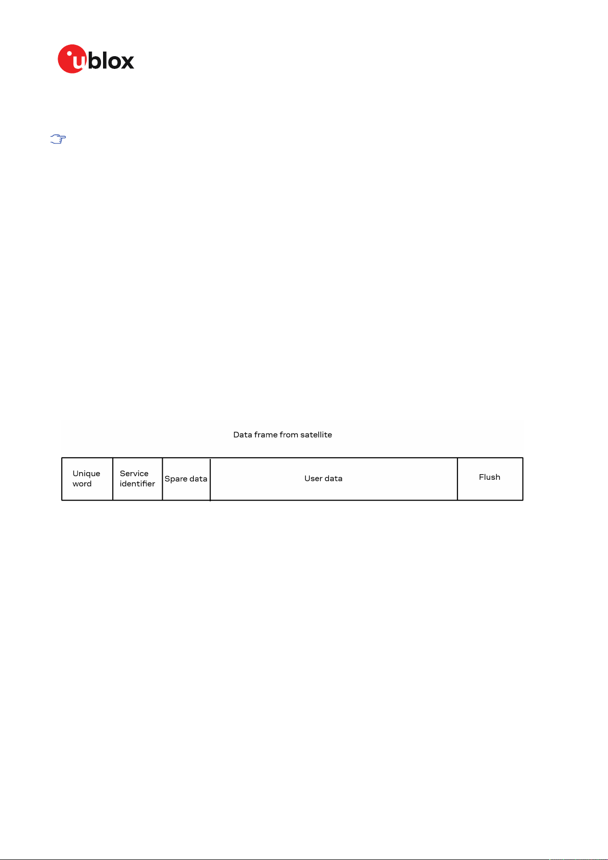
Figure 2: L band SESTB-28A data frame
3.1.6 Power management
u-blox D9 correction data receiver supports two different externally controlled power modes.
• External cycling of the receiver main power supply with the receiver in continuous mode when
powered (no battery backup software/hardware feature is supported, however V_BCKP must be
connected to VCC for correct core operation.)
• Instruct the receiver to turn on/off into software back-up mode (with main power still applied)
via the UBX-RXM-PMREQ message
3.1.6.1 Continuous mode
u-blox receivers use dedicated signal processing engines optimized for signal acquisition and
tracking. The acquisition engine delivers rapid signal searches during cold starts or when insufficient
signals are available for data download. The tracking engine delivers signal measurements for
message decoding.
UBX-19026111 - R05
C1-Public Early production information
3 Receiver functionality Page 9 of 51
Page 10
NEO-D9S-Integration manual
3.1.6.2 Power on/off command - software back-up
With message UBX-RXM-PMREQ the receiver can be forced to enter Inactive state (software backup mode) with main power still applied. It will stay in Inactive state for the time specified in the
message or until it is woken up by activity on the RXD1, NRESET pin or EXTINT pin.
3.1.6.2.1 Wake up
The receiver can be woken up by generating an edge on one of the following pins:
• Rising or falling edge on one of the EXTINT pins
• Rising or falling edge on the RXD1 pin
• Rising edge on NRESET pin
All wake-up signals are interpreted as an acquisition request, where the receiver wakes up and tries
to obtain the satellite. Wake-up signals have no effect if the receiver is already in Acquisition, Tracking
state.
3.1.6.2.2 Behavior while USB host connected
As long as the receiver is connected to a USB host, it will not enter the lowest possible power state.
This is because it must retain a small level of CPU activity to avoid breaching requirements of the
USB specification. The drawback, however, is that power consumption is higher.
Wake up by N_RESET, EXTINT pin or UART RX is possible even if the receiver is connected
to a USB host. In this case the state of the pin must be changed for a duration longer than
one millisecond.
3.2 Communication interfaces
u-blox receivers are equipped with a communication interface which is multi-protocol capable. The
interface ports can be used to transmit GNSS measurements, monitor status information and
configure the receiver.
A protocol (e.g. UBX, NMEA) can be assigned to several ports simultaneously, each configured with
individual settings (e.g. baud rate, message rates, etc.). More than one protocol (e.g. UBX protocol
and NMEA) can be assigned to a single port (multi-protocol capability), which is particularly useful
for debugging purposes.
The NEO-D9S provides UART1, UART2, SPI, I2C and USB interfaces for communication with a
host CPU. The interfaces are configured via the configuration methods described in the NEO-D9S
interface description [3].
The following table shows the port numbers reported in the UBX-MON-COMMS messages.
Port no. UBX-MON-COMMS portId Electrical interface
0 0x0000 I2C
1 0x0100 UART1
3 0x0300 USB
4 0x0400 SPI
Table 3: Port number assignment
It is important to isolate interface pins when VCC is removed. They can be allowed to float
or be connected to a high impedance (Float or tri-state: Hi-Z state). Open collector circuits
powered by module VCC are also suitable. They must be powered by module VCC to ensure
correct pin state when module VCC is removed.
Example isolation circuit is shown below.
UBX-19026111 - R05
C1-Public Early production information
3 Receiver functionality Page 10 of 51
Page 11
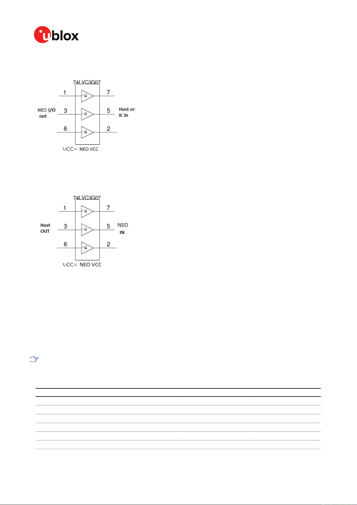
Figure 3: NEO-D9S output isolation
NEO-D9S-Integration manual
Figure 4: NEO-D9S input isolation
3.2.1 UART
A Universal Asynchronous Receiver/Transmitter (UART) port consists of an RX and a TX line. Neither
handshaking signals nor hardware flow control signals are available. The UART interface protocol
and baud rate can be configured but there is no support for setting different baud rates for reception
and transmission.
The NEO-D9S includes two UART serial ports. UART1 can be used as a host interface for
configuration, monitoring and control.
The UART RX interface will be disabled when more than 100 frame errors are detected
during a one-second period. This can happen if the wrong baud rate is used or the UART RX
pin is grounded. An error message appears when the UART RX interface is re-enabled at the
end of the one-second period.
Baud rate Data bits Parity Stop bits
9600 8 none 1
19200 8 none 1
38400 8 none 1
57600 8 none 1
115200 8 none 1
230400 8 none 1
UBX-19026111 - R05
C1-Public Early production information
3 Receiver functionality Page 11 of 51
Page 12
NEO-D9S-Integration manual
Baud rate Data bits Parity Stop bits
460800 8 none 1
921600 8 none 1
Table 4: Possible UART interface configurations
Note that for protocols such as UBX, it does not make sense to change the default word length
values (data bits) since these properties are defined by the protocol and not by the electrical
interface.
If the amount of data configured is too much for a certain port's bandwidth (e.g. all UBX messages
output on a UART port with a baud rate of 9600), the buffer will fill up. Once the buffer space is
exceeded, new messages to be sent will be dropped. To prevent message loss, the baud rate and
communication speed or the number of enabled messages should be carefully selected so that the
expected number of bytes can be transmitted in less than one second.
3.2.2 I2C interface
An I2C interface is available for communication with an external host CPU or u-blox cellular modules.
The interface can be operated in slave mode only. The I2C protocol and electrical interface are fully
compatible with the I2C industry standard fast mode. Since the maximum SCL clock frequency
is 400 kHz, the maximum transfer rate is 400 kb/s. The SCL and SDA pins have internal pull-up
resistors which should be sufficient for most applications. However, depending on the speed of the
host and the load on the I2C lines additional external pull-up resistors may be necessary.
To use the I2C interface D_SEL pin must be left open.
In designs where the host uses the same I2C bus to communicate with more than one ublox receiver, the I2C slave address for each receiver must be configured to a different value.
Typically most u-blox receivers are configured to the same default I2C slave address value.
To poll or set the I2C slave address, use the CFG-I2C-ADDRESS configuration item (see NEOD9S Interface description [3]).
The CFG-I2C-ADDRESS configuration item is an 8-bit value containing the I2C slave address
in 7 most significant bits, and the read/write flag in the least significant bit.The default value
for the CFG-I2C-ADDRESS configuration item is 0x86 (10000110). This indicates a standard
7-bit I2C slave address of 0x43 (1000011).
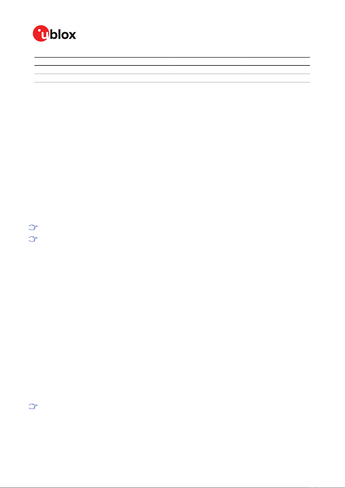
3.2.2.1 I2C register layout
The I2C interface allows 256 registers to be addressed. As shown in Figure 5, only three of these are
currently implemented.
The data registers 0 to 252 at addresses 0x00 to 0xFC contain reserved information, the result from
their reading is currently undefined. The data registers 0 to 252 are 1 byte wide.
At addresses 0xFD and 0xFE it is possible to read the currently available number of bytes.
The register at address 0xFF allows the data stream to be read. If there is no data awaiting
transmission from the receiver, then this register delivers value 0xFF, which cannot be the first byte
of a valid message. If the message data is ready for transmission, the successive reads of register
0xFF will deliver the waiting message data.
Do not use registers 0x00 to 0xFC. They are reserved for future use and they do not
currently provide any meaningful data.
UBX-19026111 - R05
C1-Public Early production information
3 Receiver functionality Page 12 of 51
Page 13
NEO-D9S-Integration manual
Figure 5: I2C register layout
3.2.2.2 Read access types
There are two I2C read transfer forms:
• The "random access" form: includes a slave register address and allows any register to be read.
• The "current address" form: omits the register address.
Figure 6 shows the format of the first one, the "random access" form of the request. Following the
start condition from the master, the 7-bit device address and the RW bit (which is a logic low for
write access) are clocked onto the bus by the master transmitter. The receiver answers with an
acknowledge (logic low) to indicate that it recognizes the address.
Next, the 8-bit address of the register to be read must be written to the bus. Following the receiver's
acknowledgment, the master again triggers a start condition and writes the device address, but this
time the RW bit is a logic high to initiate the read access. Now, the master can read 1 to N bytes
from the receiver, generating a not-acknowledge and a stop condition after the last byte being read.
UBX-19026111 - R05
C1-Public Early production information
3 Receiver functionality Page 13 of 51
Page 14

NEO-D9S-Integration manual
Figure 6: I2C random read access
If the second form, "current address" is used, an address pointer in the receiver is used to determine
which register to read. This address pointer will increment after each read unless it is already
pointing at register 0xFF, the highest addressable register, in which case it remains unaltered.
The initial value of this address pointer at start-up is 0xFF, so by default all current address reads
will repeatedly read register 0xFF and receive the next byte of message data (or 0xFF if no message
data is waiting).
Figure 7: I2C current address read access
3.2.2.3 Write access
The receiver does not provide any write access except for writing UBX and NMEA messages to the
receiver, such as configuration or aiding data. Therefore, the register set mentioned in the section
Read access is not writeable.
Following the start condition from the master, the 7-bit device address and the RW bit (which is a
logic low for write access) are clocked onto the bus by the master transmitter. The receiver answers
with an acknowledge (logic low) to indicate that it is responsible for the given address.
The master can write 2 to N bytes to the receiver, generating a stop condition after the last byte
being written. The number of data bytes must be at least 2 to properly distinguish from the write
access to set the address counter in random read accesses.
UBX-19026111 - R05
C1-Public Early production information
3 Receiver functionality Page 14 of 51
Page 15

NEO-D9S-Integration manual
Figure 8: I2C write access
3.2.3 SPI interface
The u-blox D9 correction data receiver has an SPI slave interface that can be selected by setting
D_SEL = 0. The SPI slave interface is shared with UART1 and I2C port, the physical pins are same.
The SPI pins available are:
• SPI_MISO (TXD)
• SPI_MOSI (RXD)
• SPI_CS_N
• SPI_CLK
See more information about communication interface selection from D_SEL section.
The SPI interface is designed to allow communication to a host CPU. The interface can be operated
in slave mode only.
3.2.3.1 Read access
As the register mode is not implemented for the SPI port, only the UBX/NMEA message stream is
provided. This stream is accessed using the back-to-back read and write access (see section Back-
to-back read and write access below). When no data is available to be written to the receiver, MOSI
should be held logic high, i.e. all bytes written to the receiver are set to 0xFF.
To prevent the receiver from being busy parsing incoming data, the parsing process is stopped after
50 subsequent bytes containing 0xFF. The parsing process is re-enabled with the first byte not equal
to 0xFF.
If the receiver has no more data to send, it sets MISO to logic high, i.e. all bytes transmitted decode
to 0xFF. An efficient parser in the host will ignore all 0xFF bytes which are not part of a message and
will resume data processing as soon as the first byte not equal to 0xFF is received.
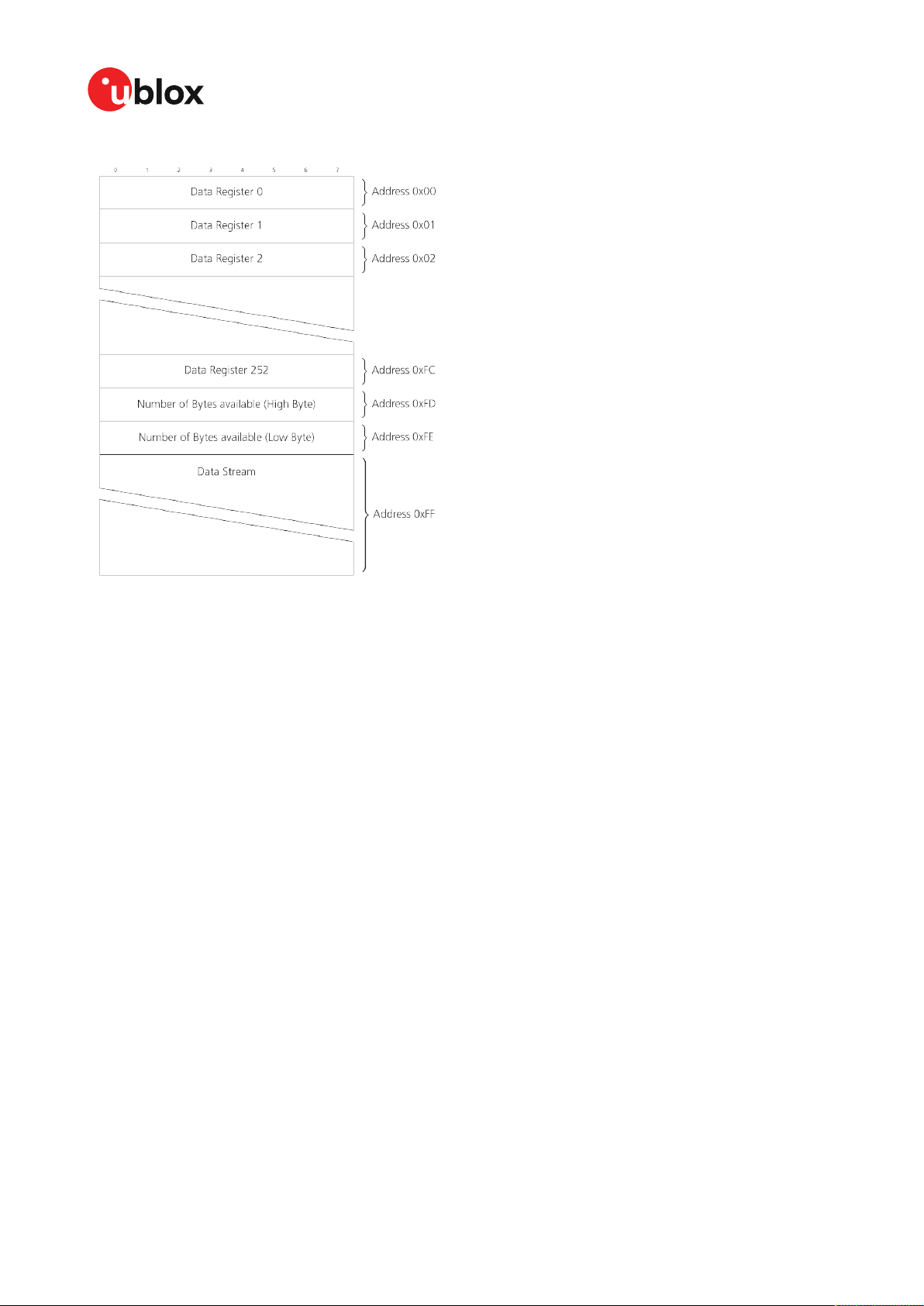
3.2.3.2 Back-to-back read and write access
The receiver does not provide any write access except for writing UBX and NMEA messages to
the receiver, such as configuration or aiding data. For every byte written to the receiver, a byte will
simultaneously be read from the receiver. While the master writes to MOSI, at the same time it needs
to read from MISO, as any pending data will be output by the receiver with this access. The data
on MISO represents the results from a current address read, returning 0xFF when no more data is
available.
UBX-19026111 - R05
C1-Public Early production information
3 Receiver functionality Page 15 of 51
Page 16
NEO-D9S-Integration manual
Figure 9: SPI back-to-back read/write access
3.2.4 USB interface
A single USB port is provided for host communication purposes.
The USB 2.0 FS (Full speed, 12 Mbit/s) interface can be used for host communication. Due to the
hardware implementation, it may not be possible to certify the USB interface.
If the receiver executes code from internal ROM (i.e. when a valid flash firmware image is not
detected), the USB behavior can differ compared to executing a firmware image from flash memory.
USB host compatibility testing is thus recommended in this scenario.
USB suspend mode is not supported.
USB bus-powered mode is not supported.
It is important to connect V_USB to ground and leave data lines open when the USB
interface is not used in an application.
The voltage range for V_USB is specified from 3.0 V to 3.6 V, which differs slightly from the
specification for VCC.
The boot screen is retransmitted on the USB port after enumeration. However, messages
generated between boot-up of the receiver and USB enumeration are not visible on the USB
port.
There are additional hardware requirements if USB is to be used:
• V_USB (pin 7) requires 1 uF capacitor mounted adjacent to the pin to ensure correct V_USB
voltage detection
• The V_USB (Pin 7) voltage should be sourced from an LDO enabled by the module VCC and
supplied from the USB host.
• A pull down resistor is required on the output of this V_USB LDO
• Pin 5 is USB_DM. Pin 6 is USB_DP.
• Apply USB_DM and USB_DP series resistors; typically 27 Ω
UBX-19026111 - R05
C1-Public Early production information
3 Receiver functionality Page 16 of 51
Page 17

NEO-D9S-Integration manual
Figure 10: NEO-D9S example circuit for USB interface
R11 = 100 k Ω is recommended
R12, R13 = 27 Ω is recommended
3.3 Predefined PIOs
In addition to the communication ports, there are some predefined PIOs provided by NEO-D9S to
interact with the receiver. These PIOs are described in this chapter.
If hardware backup mode is used a proper isolation of the interfaces is needed.
3.3.1 D_SEL
The D_SEL pin can be used to configure the functionality of the combined UART1, I2C, and SPI pins.
It is possible to configure the pins as UART1 + I2C, or as SPI. SPI is not available unless D_SEL pin
is set to low. See Table 5 below.
Pin no.
20 SPI_MISO UART1 TXD
21 SPI_MOSI UART1 RXD
18 SPI_CS_N I2C SDA
19 SPI_CLK I2C SCL
Table 5: D_SEL configuration
D_SEL == 0 D_SEL == 1
3.3.2 RESET_N
The NEO-D9S provides the ability to reset the receiver. The RESET_N pin is an input-only pin with
an internal pull-up resistor. Driving RESET_N low for at least 100 ms will trigger a cold start.
The RESET_N pin will delete all information and trigger a cold start. It should only be used
as a recovery option.
3.3.3 SAFEBOOT_N
The NEO-D9S provides a SAFEBOOT_N pin that is used to command the receiver safe boot mode.
If this pin is low at power up, the receiver starts in safe boot mode and L-band operation is disabled.
The safe boot mode can be used to recover from situations where the flash content has become
corrupted and needs to be restored.
In safe boot mode the receiver runs from a passive oscillator circuit with less accurate timing and
hence the receiver is unable to communicate via USB.
UBX-19026111 - R05
C1-Public Early production information
3 Receiver functionality Page 17 of 51
Page 18

NEO-D9S-Integration manual
In this mode only UART1 communication is possible. For communication via UART1 in safe boot
mode, the host must send a training sequence (0 x 55 55 at 9600 baud) to the receiver in order to
begin communication. After this the host must wait at least 2 ms before sending any data.
It is recommended to have the possibility to pull the SAFEBOOT_N pin low in the application. This
can be provided using an externally connected test point or a host I/O port.
3.3.4 TX_READY
This feature enables each port to define a corresponding pin, which indicates if bytes are ready to be
transmitted. A listener can wait on the TX-READY signal instead of polling the I2C or SPI interfaces.
The CFG-TXREADY message lets you configure the polarity and the number of bytes in the buffer
before the TX-READY signal goes active. By default, this feature is disabled. For USB, this feature
is configurable but might not behave as described below due to a different internal transmission
mechanism. If the number of pending bytes reaches the threshold configured for this port, the
corresponding pin will become active (configurable active-low or active-high), and stay active until
the last bytes have been transferred from software to hardware.
This is not necessarily equal to all bytes transmitted, i.e. after the pin has become inactive,
up to 16 bytes might still need to be transferred to the host.
The TX_READY pin can be selected from all PIOs which are not in use (see UBX-MON-HW3 in the
NEO-D9S Interface Description [3] for a list of the PIOs and their mapping). Each TX_READY pin is
exclusively associated to one port and cannot be shared. If PIO is invalid or already in use, only the
configuration for the specific TX_READY pin is ignored, the rest of the port configuration is applied
if valid. The acknowledge message does not indicate if the TX-READY configuration is successfully
set, it only indicates the successful configuration of the port. To validate successful configuration
of the TX_READY pin, the port configuration should be read back and the settings of TX-READY
feature verified (will be set to disabled/all zero if the settings are invalid).
The threshold when TX_READY is asserted should not be set above 2 kB as it is possible that the
internal message buffer limit is reached before this. This results in the TX_READY pin never being
set as the messages are discarded before the threshold is reached.
3.3.4.1 Extended TX timeout
If the host does not communicate over SPI or I2C for more than approximately 2 seconds, the device
assumes that the host is no longer using this interface and no more packets are scheduled for
this port. This mechanism can be changed by enabling "extended TX timeouts", in which case the
receiver delays idling the port until the allocated and undelivered bytes for this port reach 4 kB. This
feature is especially useful when using the TX-READY feature with a message output rate of less
than once per second, and polling data only when data is available, determined by the TX_READY
pin becoming active.
3.3.5 EXTINT
EXTINT is an external interrupt pin with fixed input voltage thresholds with respect to VCC. It is used
in software back-up mode to wake the module. Leave open if unused, this function is disabled by
default.
3.4 Antenna supervisor
An active antenna supervisor provides the means to check the antenna for open and short circuits
and to shut off the antenna supply if a short circuit is detected. Once enabled, the active antenna
supervisor produces status messages, reporting in NMEA and/or UBX protocol.
UBX-19026111 - R05
C1-Public Early production information
3 Receiver functionality Page 18 of 51
Page 19

NEO-D9S-Integration manual
The antenna supervisor can be configured through the CFG-HW-ANT_* configuration items. The
current configuration of the active antenna supervisor can also be checked by polling the related
CFG-HW_ANT_* configuration items.
The current active antenna status can be determined by polling the UBX-MON-RF message. If an
antenna is connected, the initial state after power-up is “Active Antenna OK" in the UBX-MON-RF
message in the u-center "Message View".
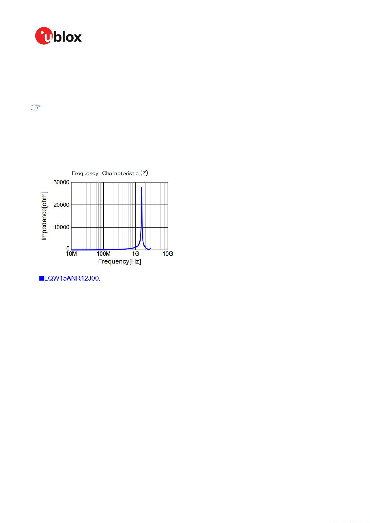
An active antenna supervisor circuit is connected to the ANT_DET, ANT_OFF, ANT_SHORT_N
pins. For an example the open circuit detection circuit using ANT_DET, "high" = Antenna detected
(antenna consumes current); "low" = Antenna not detected (no current drawn).
The following schematic details the required circuit and the sections following it explain how to
enable and monitor each feature:
Figure 11: NEO-D9S antenna supervisor
The bias-t inductor must be chosen for multi-band operation; a value of 47 nH ±5% is
required for our recommended Murata part, with the current limited below its 300 mA
rating. See Antenna bias section for additional information.
Circuit shows buffer [U4]. Buffer is not strictly necessary when supplied from VCC. It is only
required when supplying antenna voltage that is not obtained from or controlled by module
VCC or VCC_RF .
ESD diode not shown in the image above, it is mounted close to the PCB RF connector.
Part Recommendation Comment
L1 Murata LQG15HS47NJ02/47N 300mA and >500 Ω at L band frequencies
C2 Murata GRM033R71C103KE14 CAP CER X7R 0402 10N 10% 16V
UBX-19026111 - R05
C1-Public Early production information
3 Receiver functionality Page 19 of 51
Page 20

NEO-D9S-Integration manual
Part Recommendation Comment
TYCO, 0.25PF, PESD0402-140 -55/+125C ESD protection diode on RF trace
Table 6: Recommended components for antenna supervisor
3.4.1 Antenna voltage control - ANT_OFF
Antenna status (as reported in UBX-MON-RF and UBX-INF-NOTICE messages) is not
reported unless the antenna voltage control has been enabled.
Enable the antenna voltage control by setting the configuration item CFG-HWANT_CFG_VOLTCTRL to true (1).
Result:
• UBX-MON-RF in u-center "Message View": Antenna status = OK. Antenna power status = ON
• ANT_OFF pin = active high to turn antenna off therefore the pin is low to enable an external
antenna.
Start-up message at power up if configuration stored:
$GNTXT,01,01,02,ANTSUPERV=AC *00
$GNTXT,01,01,02,ANTSTATUS=INIT*3B
$GNTXT,01,01,02,ANTSTATUS=OK*25
ANTSUPERV=AC indicates antenna control is activated
3.4.2 Antenna short detection - ANT_SHORT_N
Enable the antenna short detection by setting the configuration item CFG-HWANT_CFG_SHORTDET to true (1).
Result:
• UBX-MON-RF in u-center "Message View": Antenna status = OK. Antenna power status = ON
• ANT_OFF = active high to disable an external antenna therefore the pin is low to enable an
external antenna.
• ANT_SHORT_N = active low to detect a short therefore the pin is high (PIO pull up enabled to be
pulled low if shorted)
Start-up message at power up if configuration is stored:
$GNTXT,01,01,02,ANTSUPERV=AC SD *37
$GNTXT,01,01,02,ANTSTATUS=INIT*3B
$GNTXT,01,01,02,ANTSTATUS=OK*25
ANTSUPERV=AC SD (Antenna control and short detection activated)
Then if shorted (ANT_SHORT_N pulled low):
• UBX-MON-RF in u-center "Message View": Antenna status = SHORT. Antenna power status =
ON (Antenna power control power down when short has not been enabled = off by default).
$GNTXT,01,01,02,ANTSTATUS=SHORT*73
• ANT_OFF = active high therefore still low (still enabled as auto power down is not enabled)
After a detected antenna short, the reported antenna status will keep on being reported as
shorted. If the antenna short detection auto recovery is enabled, then the antenna status
UBX-19026111 - R05
C1-Public Early production information
3 Receiver functionality Page 20 of 51
Page 21

NEO-D9S-Integration manual
can recover after a timeout. To recover the antenna status immediately, a power cycle is
required or configuring the antenna short detection functionality off and on.
3.4.3 Antenna short detection auto recovery
Enable the antenna short detection auto recovery by setting the configuration item CFG-HWANT_CFG_RECOVER to true (1).
Result:
• UBX-MON-RF in u-center "Message View": Antenna status = OK. Antenna power status = ON
• ANT_OFF = active high there for the PIO is low to enable an external antenna
• ANT_SHORT_N = high (PIO pull up enabled to be pulled low if shorted)
Start-up message at power up if configuration is stored:
$GNTXT,01,01,02,ANTSUPERV=AC SD PDoS SR*3E
$GNTXT,01,01,02,ANTSTATUS=INIT*3B
$GNTXT,01,01,02,ANTSTATUS=OK*25
ANTSUPERV=AC SD PDoS SR (indicates short circuit recovery added - SR)
Then if antenna is shorted (ANT_SHORT_N pulled low):
•
$GNTXT,01,01,02,ANTSTATUS=SHORT*73
• UBX-MON-RF in u-center "Message View": Antenna status = SHORT. Antenna power status =
OFF
• ANT_OFF = high (to disable - active high)
After a time out period receiver will re-test the short condition by enabling ANT_OFF = LOW
If a short is not present it will report antenna condition is OK:
$GNTXT,01,01,02,ANTSTATUS=OK*25
UBX-MON-RF in u-center "Message View": Antenna status = OK. Antenna power status = ON
3.4.4 Antenna open circuit detection - ANT_DETECT
Enable the antenna open circuit detection by setting the configuration item CFG-HWANT_CFG_OPENDET to true (1).
Result:
• UBX-MON-RF in u-center "Message View": Antenna status = OK. Antenna power status = ON
• ANT_OFF = active high therefore PIO is low to enable external antenna
• ANT_SHORT_N = active low therefore PIO is high (PIO pull up enabled to be pulled low if
shorted)
• ANT_DETECT = active high therefore PIO is high (PIO pull up enabled to be pulled low if antenna
not detected)
Start-up message at power up if configuration is stored:
$GNTXT,01,01,02,ANTSUPERV=AC SD OD PDoS SR*15
$GNTXT,01,01,02,ANTSTATUS=INIT*3B
$GNTXT,01,01,02,ANTSTATUS=OK*25
ANTSUPERV=AC SD OD PDoS SR (indicates open circuit detection added - OD)
UBX-19026111 - R05
C1-Public Early production information
3 Receiver functionality Page 21 of 51
Page 22

NEO-D9S-Integration manual
Then if ANT_DETECT is pulled low to indicate no antenna:
$GNTXT,01,01,02,ANTSTATUS=OPEN*35
Then if ANT_DETECT is left floating or it is pulled high to indicate antenna connected:
$GNTXT,01,01,02,ANTSTATUS=OK*25
3.5 Security
3.5.1 Receiver status monitoring
Messages in the UBX class UBX-MON are used to report the status of the parts of the embedded
computer system that are not related to the received satellite system specific info.
The main purposes are:
• Hardware and software versions, using UBX-MON-VER.
3.6 Forcing a receiver reset
The NEO-D9S is not a GNSS receiver and does not operate to the same principles as a standard
GNSS. However it does support the standard UBX-CFG-RST command.
Data stored in flash memory is not cleared by any of the options provided by UBX-CFG-RST.
The resetMode must be specified. This is not related to L band, but to the way the software restarts
the system.
• Hardware reset (watchdog), immediately uses the on-chip watchdog, in order to electrically
reset the chip. This is an immediate, asynchronous reset. No Stop events are generated.
• Controlled software reset terminates all running processes in an orderly manner and, once the
system is idle, restarts operation, reloads its configuration and starts to acquire and track L
band satellites.
• Hardware reset (watchdog), after shutdown uses the on-chip watchdog, in order to electrically
reset the chip after shutdown.
3.7 Firmware upload
NEO-D9S is supplied with firmware. u-blox may release updated images containing, for example,
security fixes, enhancements, bug fixes, etc. Therefore it is important that customers implement a
firmware update mechanism in their system.
A firmware image is a binary file containing the software to be run by the GNSS receiver. A firmware
update is the process of transferring a firmware image to the receiver and storing it in non-volatile
flash memory.
Contact u-blox for more information on firmware update.
UBX-19026111 - R05
C1-Public Early production information
3 Receiver functionality Page 22 of 51
Page 23

NEO-D9S-Integration manual
4 Design
This section provides information to help carry out a successful schematic and PCB design
integrating the NEO-D9S.
4.1 Pin assigment
The pin assignment of the NEO-D9S module is shown in Figure 12. The defined configuration of the
PIOs is listed in Table 7.
UART2, V_BCKP software function, are not available in the current software version.
V_BCKP hardware pin must be connected to VCC to ensure correct hardware operation.
UART2 is reserved for future direct connection to u-blox F9 high precision GNSS receivers. It will be
enabled in following FW versions.
Do not permanently connect the NEO-D9S UART2 with the ZED-F9 UART2 as the current
software in both modules does not support this. A conflict could possibly occur with the
default software settings in both modules. Instead, provide a jumper to connect the two
UART2 ports when the firmware is supported.
Figure 12: NEO-D9S pin assignment
Pin no. Name I/O Description
1 SAFEBOOT_N I SAFEBOOT_N (used for FW updates and reconfiguration, leave open)
2 D_SEL I UART 1 / SPI select. (open or high = UART 1)
3 TXD2 O UART 2 TXD
4 RXD2 I UART 2 RXD
5 USB_DM I/O USB data (DM)
UBX-19026111 - R05
C1-Public Early production information
4 Design Page 23 of 51
Page 24

NEO-D9S-Integration manual
Pin no. Name I/O Description
6 USB_DP I/O USB data (DP)
7 V_USB I USB supply
8 RESET_N I RESET (active low)
9 VCC_RF O External LNA power
10 GND I Ground
11 RF_IN I Active antenna L band signal input
12 GND I Ground
13 GND I Ground
14 ANT_OFF O External LNA disable - default active high
15 ANT_DETECT I Active antenna detect - default active high
16 ANT_SHORT_N O Active antenna short detect- default active low
17 EXTINT I External interrupt pin
18 SDA / SPI CS_N I/O I2C data if D_SEL = VCC (or open); SPI chip select if D_SEL = GND
19 SCL / SPI SLK I/O I2C clock if D_SEL = VCC (or open); SPI clock if D_SEL = GND
20 TXD / SPI MISO O UART output if D_SEL = VCC (or open); SPI MISO if D_SEL = GND
21 RXD / SPI MOSI I UART input if D_SEL = VCC (or open); SPI MOSI if D_SEL = GND
22 V_BCKP I Connect to VCC
23 VCC I Supply voltage
24 GND I Ground
Table 7: NEO-D9S pin assigment
4.2 Antenna
u-blox mandates the use of an active antenna for the NEO-D9S. The NEO-D9S needs to receive L
band signals in order to operate.
A separate L band antenna should be used to meet the requirement of +4 dBic patch
element gain.
A suitable ground plane is required for the antenna to achieve good performance for the L
band antenna.
Location of the antenna is critical for reaching good performance.
Figure 13: Typical L band active antenna structure
UBX-19026111 - R05
C1-Public Early production information
4 Design Page 24 of 51
Page 25

NEO-D9S-Integration manual
Figure 14: Typical recommended separate NEO-D9S and ZED-F9P RF front end and system
L band refers to the operating frequency range of 1–2 GHz in the radio spectrum. However in this
case we are referring to a corrections receiver that can operate at 1525.0 - 1559.0 MHz. The active
antenna must be selected for the required corrections band. Open jumper for UART2 is for future
firmware versions. It must not be connected by default.
An LNA gain of 20 - 25 dB is recommended to reach the ZED-F9P and NEO-D9S RF_IN pins.
For more information on the ZED-F9P design in and interfaces see the ZED-F9P Integration Manual
[4].
Recommended single L band antenna required specifications
Parameter Specification
Antenna type Active antenna
Typical gain 30 dB
Maximum gain 40 dBActive antenna recommendations
Maximum noise figure 3 dB
L band antenna gain
Polarization RHCP
1
Measured with a ground plane d=150 mm
2
The recommended gain is important for good performance
1
1525 MHz - 1559 MHz: 4 dBic typical in the L
2
band
UBX-19026111 - R05
C1-Public Early production information
4 Design Page 25 of 51
Page 26
NEO-D9S-Integration manual
Parameter Specification
Axial ratio 2 dB max at zenith
EMI immunity out-of-band
3
30 V/m
Out-of-band Rejection 40 dB typ
ESD circuit protection 15 kV human body model air discharge
Table 8: Antenna specifications for NEO-D9S modules
It is not recommended to use a combined antenna due to limitations of combined patch element
gain for L band. However if this is still a consideration the combined required specification is detailed
below:
Combined L1 + L2 + L band active antenna required specifications
Parameter Specification
Antenna type Active antenna
Typical gain 30 dB
Maximum gain 40 dBActive antenna recommendations
Maximum noise figure 2 dB
L1/L band band antenna gain
L2/E5b band antenna gain
4
6
Polarization RHCP
Axial ratio 2 dB max at zenith
Phase center variation <10 mm over elevation/azimuth
Group delay variation in-band
EMI immunity out-of-band
7
8
Out-of-band 9 Rejection
ESD circuit protection 15 kV human body model air discharge
Table 9: Antenna specifications for NEO-D9S modules
1525 - 1606 MHz: 3 dBic typ, 4 dBic typical in L
5
band
1197 - 1249 MHz: 2 dBic typ.
10 ns max at each GNSS system bandwidth. Note:
Inter-signal requirement 50 ns max.
30 V/m
40 dB typ
Recommended L band C/N0 levels
Baud rate Target C/N0 level Target optimized
600 37 dBHz 40 dBHz
1200 40 dBHz 43 dBHz
2400 43 dBHz 46 dBHz
Table 10: C/N0 specifications for NEO-D9S modules
3
Exception L1 and L2 bands +/- 200 MHz, emphasis on cellular bands
4
Measured with a ground plane d=150 mm
5
The recommended gain is important for good performance
6
Measured with a ground plane d=150 mm
7
GNSS system bandwidths: 1559… 1563 MHz; 1573… 1578 MHz; 1598… 1606 MHz; 1192… 1212 MHz; 1197… 1217
MHz; 1223… 1231 MHz; 1242… 1249 MHz
8
Exception L1 and L2 bands +/- 200 MHz, emphasis on cellular bands
9
GNSS system bandwidths: 1559… 1563 MHz; 1573… 1578 MHz; 1598… 1606 MHz; 1192… 1212 MHz; 1197… 1217
MHz; 1223… 1231 MHz; 1242… 1249 MHz
UBX-19026111 - R05
C1-Public Early production information
4 Design Page 26 of 51
C/N0 level
Page 27
NEO-D9S-Integration manual
The antenna system should include filtering to ensure adequate protection from nearby
transmitters. Care should be taken in the selection of antennas placed close to cellular or Wi-Fi
transmitting antennas.
4.2.1 Antenna bias
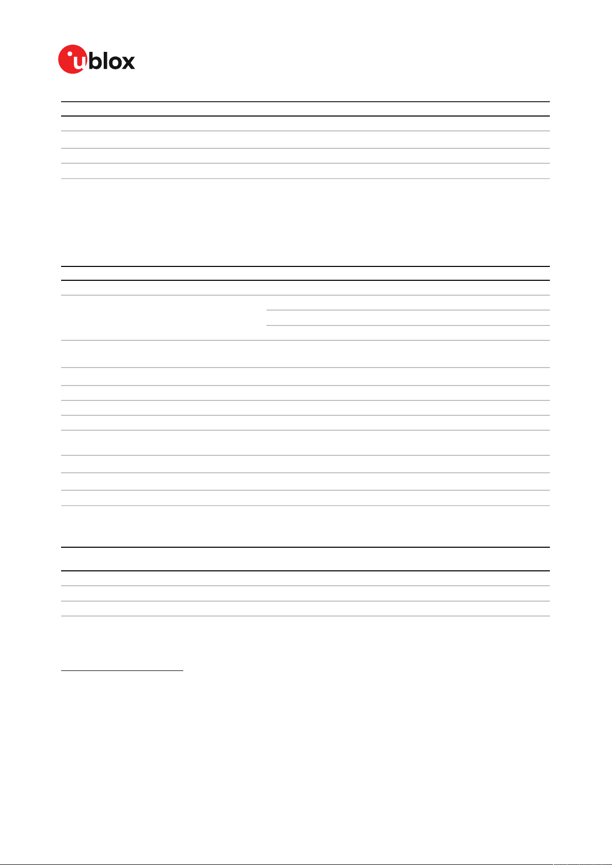
The bias-t inductor must be chosen for multi-band operation, a value of 47 nH ±5% is
recommended for the recommended Murata L part. It has a self-resonance frequency of 1
GHz and a high impedance (> 500 Ω) at L band frequencies.
The recommended bias-t inductor (Murata LQG15HS47NJ02) has a maximum current capacity of
300 mA. Hence the current is limited to 70 mA at 3.3V using an active limiter in the recommended
circuit shown in Figure 16 below. A 10 Ω resistor (R2) is provided to measure the current. This resistor
power rating must be chosen to ensure reliability in the chosen circuit design.
Figure 15: NEO-D9S antenna bias inductor impedance
A recommended circuit design for an active antenna bias is shown below. This example shows an
external voltage of 3.3 V with current limiting as described above. An ESD protection diode should
also be connected to the input as shown.
UBX-19026111 - R05
C1-Public Early production information
4 Design Page 27 of 51
Page 28

NEO-D9S-Integration manual
Figure 16: NEO-D9S reference design for antenna bias
L1: Murata LQG15HS47NJ02 0402 47 N 5% 0.30 A -55/+125 C
D1: TYCO, 0.25PF, PESD0402-140 -55/+125C
C3: Murata GRM155R61A104KA01 CER X5R 0402 100N 10% 10V
R2: RES THICK FILM CHIP 1206 10R 5% 0.25W
It is recommended to use active current limiting. If active current limiting is not used, the important
points covered below need to be taken into account:
Figure 17: NEO-D9S VCC_RF antenna bias
The bias-t inductor and current limiting resistor must be selected to be reliable with a shortcircuit on the antenna feed if no active current limiter is used. Our recommended part has
a limit of 300 mA. A part with a higher current capability will be needed if the short circuit
current is as described here. This will also be affected by the voltage level of the antenna
UBX-19026111 - R05
C1-Public Early production information
4 Design Page 28 of 51
Page 29
NEO-D9S-Integration manual
bias supply due to power dissipation. Take the current limit capability of the antenna bias
supply into consideration. In the case where the module supplies the voltage via VCC_RF, a
higher value resistor will be needed to ensure the module supply inductor is protected. The
current should be limited to below 150 mA at the module supply voltage under short-circuit
conditions. In this case a value of 17 Ω or more is required at a module supply of 3 V to limit
short circuit current to 150 mA. The DC resistance of the bias-t inductor is assumed to be
1-2 Ω and the module internal feed inductor is assumed to be 1.2 Ω.
If the VCC_RF voltage does not match with the supply voltage of the active antenna, use a filtered
external supply.
The power dissipation in the resistor and inductor needs to be taken into account based on
the supply voltage and short circuit current. The bias-t inductor current capability and the
bias resistor value need to be calculated as shown above. The supply voltage for the bias-t
and its current capability is part of the calculation.
Figure 18: NEO-D9S external voltage antenna bias
4.3 Power supply
The u-blox NEO-D9S module has two power supply pins: VCC and V_USB.
4.3.1 VCC: Main supply voltage
The VCC pin is connected to the main supply voltage. During operation, the current drawn by the
module can vary by some orders of magnitude. For this reason, it is important that the supply
circuitry be able to support the peak power for a short time (see the NEO-D9S Data sheet [1] for
specification).
To reduce peak current during power on, users can employ an LDO that has an in-built
current limiter.
Do not add any series resistance greater than 0.2 Ω to the VCC supply as it will generate
input voltage noise due to dynamic current conditions.
For the NEO-D9S module the equipment must be supplied by an external limited power
source in compliance with the clause 2.5 of the standard IEC 60950-1.
4.3.2 NEO-D9S power supply
The NEO-D9S requires a low-noise, low-dropout voltage, and a very low source impedance power
supply of 3.3 V typically. No inductors or ferrite beads should be used from LDO to the module
VCC pin. The peak currents need to be taken into account for the source supplying the LDO for the
module.
UBX-19026111 - R05
C1-Public Early production information
4 Design Page 29 of 51
Page 30
NEO-D9S-Integration manual
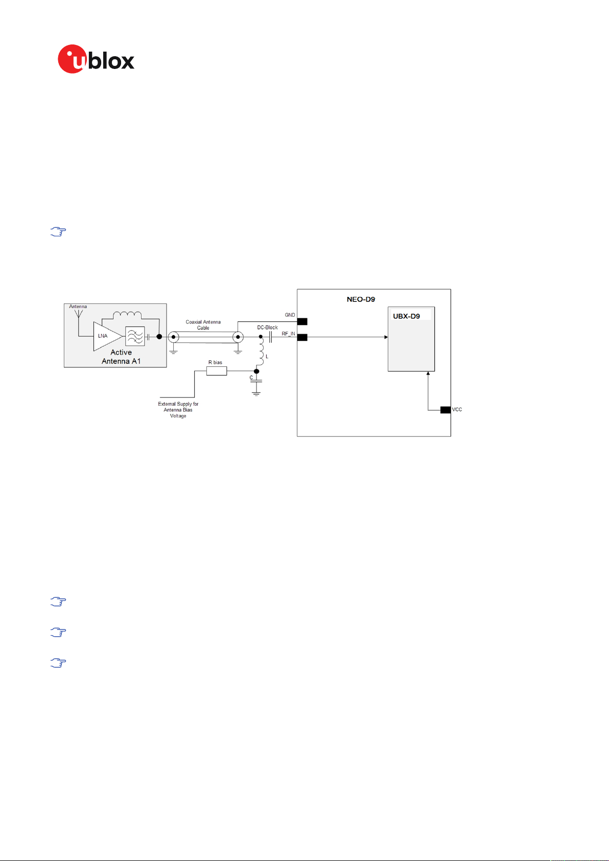
A power supply fed by 5 V is shown in the figure below. This example circuit is intended only for the
module supply.
Figure 19: NEO-D9S power supply
4.4 NEO-D9S minimal design
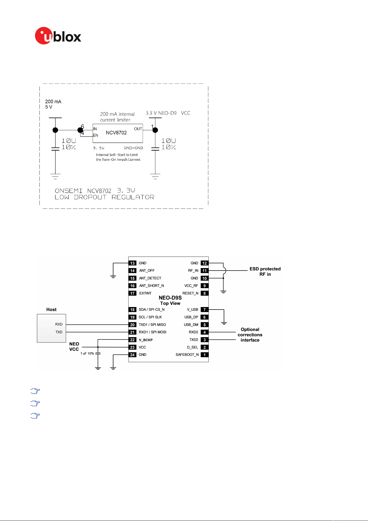
The minimal electrical circuit for NEO-D9S operation using the UART1 interface is shown below:
Figure 20: Minimal NEO-D9S design
It is important to connect V_USB to ground if USB is not used.
UART2 software functionality will be available in a later firmware update.
Connect the power supply to VCC and V_BCKP.
4.5 EOS/ESD precautions
When integrating L-band receivers into wireless systems, careful consideration must be given to
electromagnetic and voltage susceptibility issues. Wireless systems include components which
can produce Electrostatic Discharge (ESD), Electrical Overstress (EOS) and Electro-Magnetic
UBX-19026111 - R05
C1-Public Early production information
4 Design Page 30 of 51
Page 31
NEO-D9S-Integration manual
Interference (EMI). CMOS devices are more sensitive to such influences because their failure
mechanism is defined by the applied voltage, whereas bipolar semiconductors are more susceptible
to thermal overstress. The following design guidelines are provided to help in designing robust yet
cost-effective solutions.
To avoid overstress damage during production or in the field it is essential to observe strict
EOS/ESD/EMI handling and protection measures.
To prevent overstress damage at the RF_IN of your receiver, never exceed the maximum
input power as specified in the u-blox NEO-D9S Data sheet [1].
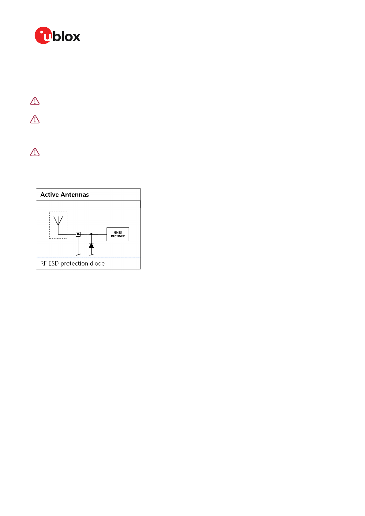
4.5.1 ESD protection measures
L-band receivers are sensitive to Electrostatic Discharge (ESD). Special precautions are
required when handling. Most defects caused by ESD can be prevented by following strict
ESD protection rules for production and handling. When implementing passive antenna
patches or external antenna connection points, then additional ESD measures as shown in
the figure below can also avoid failures in the field.
Figure 21: RF ESD precautions
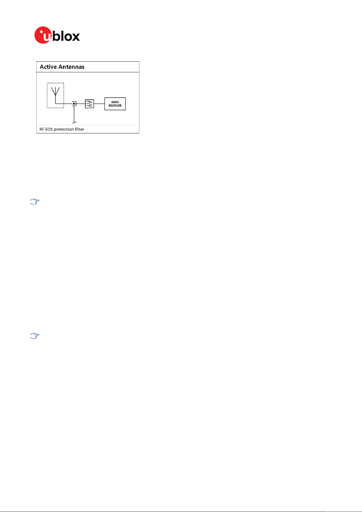
4.5.2 EOS precautions
Electrical overstress (EOS) usually describes situations when the maximum input power exceeds
the maximum specified ratings. EOS failure can happen if RF emitters are close to a L-band receiver
or its antenna. EOS causes damage to the chip structures. If the RF_IN is damaged by EOS, it is hard
to determine whether the chip structures have been damaged by ESD or EOS.
EOS protection measures as shown in the figure below are recommended for any designs combining
wireless communication transceivers (e.g. GSM, GPRS) and L-band in the same design or in close
proximity.
UBX-19026111 - R05
C1-Public Early production information
4 Design Page 31 of 51
Page 32
NEO-D9S-Integration manual
Figure 22: Active antenna EOS protection
4.5.3 Safety precautions
The NEO-D9S must be supplied by an external limited power source in compliance with the clause
2.5 of the standard IEC 60950-1. In addition to external limited power source, only Separated or
Safety Extra-Low Voltage (SELV) circuits are to be connected to the module including interfaces and
antennas.
For more information about SELV circuits see section 2.2 in Safety standard IEC 60950-1.
4.6 Electromagnetic interference on I/O lines
Any I/O signal line with a length greater than approximately 3 mm can act as an antenna and may
pick up arbitrary RF signals transferring them as noise into the receiver. This specifically applies to
unshielded lines, in which the corresponding GND layer is remote or missing entirely, and lines close
to the edges of the printed circuit board.
If, for example, a cellular signal radiates into an unshielded high-impedance line, it is possible to
generate noise in the order of volts and not only distort receiver operation but also damage it
permanently. Another type of interference can be caused by noise generated at the PIO pins that
emits from unshielded I/O lines. Receiver performance may be degraded when this noise is coupled
into the L-band antenna.
EMI protection measures are particularly useful when RF emitting devices are placed next to the
L-band receiver and/or to minimize the risk of EMI degradation due to self-jamming. An adequate
layout with a robust grounding concept is essential in order to protect against EMI.
Intended Use: In order to mitigate any performance degradation of a radio equipment under
EMC disturbance, system integration shall adopt appropriate EMC design practice and not
contain cables over three meters on signal and supply ports.
4.6.1 General notes on interference issues
Received L-band signal power at the antenna is very low. At the nominal received signal strength
(-128 dBm) it is below the thermal noise floor of -111 dBm. Due to this fact, a L-band receiver is
susceptible to interference from nearby RF sources of any kind. Two cases can be distinguished:
• Out-of-band interference: Typically any kind of wireless communications system (e.g. LTE,
GSM, CDMA, 3G, WLAN, Bluetooth, etc.) may emit its specified maximum transmit power in
close proximity to the L-band receiving antenna, especially if such a system is integrated with
the L-band receiver. Even at reasonable antenna selectivity, destructive power levels may reach
the RF input of the L-band receiver. Also, larger signal interferers may generate intermodulation
products inside the L-band receiver front-end that fall into the L-band band and contribute to
in-band interference.
UBX-19026111 - R05
C1-Public Early production information
4 Design Page 32 of 51
Page 33

NEO-D9S-Integration manual
• In-band interference: Although the L-band band is kept free from intentional RF signal sources
by radio-communications standards, many devices emit RF power into the L-band band at
levels much higher than the L-band signal itself. One reason is that the frequency band above
1 GHz is not well regulated with regards to EMI, and even if permitted, signal levels are much
higher than L-band signal power. Notably, all types of digital equipment, such as PCs, digital
cameras, LCD screens, etc. tend to emit a broad frequency spectrum up to several GHz of
frequency. Also wireless transmitters may generate spurious emissions that fall into L-band
band.
As an example, GSM uses power levels of up to 2 W (+33 dBm). The absolute maximum power input
at the RF input of the L-band receiver can be +15 dBm. The GSM specification allows spurious
emissions for GSM transmitters of up to +36 dBm, while the L-band signal is less than -128
dBm. By simply comparing these numbers it is obvious that interference issues must be seriously
considered in any design of a L-band receiver. Different design goals may be achieved through
different implementations:
• The primary focus is to prevent damaging the receiver from large input signals. Here the Lband performance under interference conditions is not important and suppression of the
signal is permitted. It is sufficient to just observe the maximum RF power ratings of all of the
components in the RF input path.
• L-band performance must be guaranteed even under interference conditions. In such a case,
not only the maximum power ratings of the components in the receiver RF path must be
observed. Further, non-linear effects like gain compression, NF degradation (desensitization)
and intermodulation must be analyzed.
Pulsed interference with a low-duty cycle such as GSM may be destructive due to the high
peak power levels.
4.6.2 In-band interference mitigation
With in-band interference, the signal frequency is very close to the L-band frequency. Such
interference signals are typically caused by harmonics from displays, micro-controller operation, bus
systems, etc. Measures against in-band interference include:
• Maintaining a good grounding concept in the design
• Shielding
• Layout optimization
• Low-pass filtering of noise sources, e.g. digital signal lines
• Remote placement of the L-band antenna, far away from noise sources
• Adding an LTE, CDMA, GSM, WCDMA, BT band-pass filter before antenna
4.6.3 Out-of-band interference
Out-of-band interference is caused by signal frequencies that are different from the L-band carrier
frequency. The main sources are wireless communication systems such as LTE, GSM, CDMA,
WCDMA, Wi-Fi, BT, etc.
Measures against out-of-band interference include maintaining a good grounding concept in the
design and adding a L-band band-pass filter into the antenna input line to the receiver.
For GSM applications, such as typical handset design, an isolation of approximately 20 dB can be
reached with careful placement of the antennas. If this is insufficient, an additional SAW filter is
required on the L-band receiver input to block the remaining GSM transmitter energy.
UBX-19026111 - R05
C1-Public Early production information
4 Design Page 33 of 51
Page 34

NEO-D9S-Integration manual
4.7 Layout
This section details layout and placement requirements of the u-blox D9 correction data receiver.
4.7.1 Placement
L-band signals at the surface of the Earth are below the thermal noise floor. A very important
factor in achieving maximum GNSS performance is the placement of the receiver on the PCB. The
placement used may affect RF signal loss from antenna to receiver input and enable interference
into the sensitive parts of the receiver chain, including the antenna itself. When defining a GNSS
receiver layout, the placement of the antenna with respect to the receiver, as well as grounding,
shielding and interference from other digital devices are crucial issues and need to be considered
very carefully.
Signal loss on the RF connection from antenna to receiver input must be minimized as much as
possible. Hence, the connection to the antenna must be kept as short as possible.
Ensure that RF critical circuits are clearly separated from any other digital circuits on the system
board. To achieve this, position the receiver digital part closer to the digital section of the system
PCB and have the RF section and antenna placed as far as possible away from the other digital
circuits on the board.
A proper GND concept shall be followed: The RF section shall not be subject to noisy digital supply
currents running through its GND plane.
4.7.2 Thermal management
During design-in do not place the receiver near sources of heating or cooling. The receiver oscillator
is sensitive to sudden changes in ambient temperature which can adversely impact satellite signal
tracking. Sources can include co-located power devices, cooling fans or thermal conduction via the
PCB. Take into account the following questions when designing in the receiver.
• Is the receiver placed away from heat sources?
• Is the receiver placed away from air-cooling sources?
• Is the receiver shielded by a cover/case to prevent the effects of air currents and rapid
environmental temperature changes?
High temperature drift and air vents can affect the GNSS performance. For best
performance, avoid high temperature drift and air vents near the receiver.
4.7.3 Package footprint, copper and paste mask
Copper and solder mask dimensioning recommendations for the NEO-D9S module packages are
provided in this section.
The module edge pads are 0.8 mm x 0.9 mm. Implement a pad size on your PCB as a copper
pad size of 0.8 mm x 1.8 mm. Solder mask for the same pad is 0.9 mm x 1.9 mm. Paste
mask for the same pad is 0.8 mm x 2.1 mm.
These are recommendations only and not specifications. Consider the paste mask outline
when defining the minimal distance to the next component. The exact copper, solder and
paste mask geometries, distances, stencil thickness and solder paste volumes must be
adapted to the specific production processes (e.g. soldering etc.) of the customer.
UBX-19026111 - R05
C1-Public Early production information
4 Design Page 34 of 51
Page 35

4.7.3.1 Mechanical dimensions
NEO-D9S-Integration manual
Figure 23: NEO-D9S mechanical dimensions
4.7.3.2 Footprint
Figure 24: NEO-D9S suggested footprint (i.e. copper mask)
UBX-19026111 - R05
C1-Public Early production information
4 Design Page 35 of 51
Page 36

4.7.3.3 Paste mask
Figure 25: NEO-D9S suggested paste mask
NEO-D9S-Integration manual
To improve the wetting of the half vias, reduce the amount of solder paste under the module and
increase the volume outside of the module by defining the dimensions of the paste mask to form a
T-shape (or equivalent) extending beyond the copper mask.
4.7.4 Layout guidance
The presented layout guidance reduces the risk of performance issues at design level.
4.7.4.1 RF In trace
The RF In trace has to work in the middle L band frequencies.
For FR-4 PCB material with a dielectric permittivity of for example 4.7, the trace width for the 50 Ω
line impedance can be calculated.
Figure 26: Microstrip trace width
A grounded co-planar RF trace is recommended as it provides the maximum shielding from noise
with adequate vias to the ground layer.
UBX-19026111 - R05
C1-Public Early production information
4 Design Page 36 of 51
Page 37

NEO-D9S-Integration manual
Figure 27: Grounded co-planar RF trace
The RF trace must be shielded by vias to ground along the entire length of the trace and the NEOD9S RF_IN pad should be surrounded by vias as shown in the figure below.
Figure 28: RF input trace
The RF_IN trace on the top layer should be referenced to a suitable ground layer.
UBX-19026111 - R05
C1-Public Early production information
4 Design Page 37 of 51
Page 38

NEO-D9S-Integration manual
4.7.4.2 VCC pad
The VCC pad for the u-blox D9 correction data receiver needs to have as low an impedance as
possible with large vias to the lower power layer of the PCB. The VCC pad needs a large pad and the
decoupling capacitor must be placed as close as possible. This is shown in the figure below.
Figure 29: VCC pad
4.8 Design guidance
4.8.1 General considerations
Check power supply requirements and schematic:
• Is the power supply voltage within the specified range and noise-free?
• If USB is not used, connect the V_USB pin to ground.
• It is recommended to have a separate LDO for V_USB that is enabled by the module VCC. This is
to comply with the USB self-powered specification.
• If USB is used, is there a 1 uF capacitor right near the V_USB pin? This is just for the V_USB pin.
• Is there a 1 uF cap right next to the module VCC pin?
• Connect the power supply to VCC and V_BCKP.
• Compare the peak current consumption of the NEO-D9S L-band module with the specification
of your power supply.
• L-band receivers require a stable power supply. Avoid series resistance (less than 0.2 Ω) in
your power supply line (the line to VCC) to minimize the voltage ripple on VCC. See the NEOD9S Power supply section in the Design chapter for more information on the power supply
requirements.
• All I/O (including UART) must not be pulled high before power ON.
• Any pull ups must be tied to module VCC to ensure they are at the correct state on power ON
and OFF.
• Allow all I/O to Float/High impedance (High-Z) when VCC is not applied.
4.8.2 RF front-end circuit options
It is mandatory that the RF input is fed by an active antenna meeting the requirements for
the NEO-D9S.
The first stages of the signal processing chain are crucial to the overall receiver performance.
When an RF input connector is employed this can provide a conduction path for harmful or
destructive electrical signals. If this is a likely factor the RF input should be protected accordingly.
Additional points on the RF input
• What is the expected quality of the signal source (antenna)?
UBX-19026111 - R05
C1-Public Early production information
4 Design Page 38 of 51
Page 39
NEO-D9S-Integration manual
• What is the external active antenna signal power?
• What is the bandwidth and filtering of the external active antenna?
• Does the L band external antenna meet the recommended +4 dBic patch element gain for the
1525 MHz - 1559 MHz band?
Are destructive RF power levels expected to reach the RF input? Is interference from wireless
transmitters expected?
• What are the characteristics of these signals (duty cycle, frequency range, power range,
spectral purity)?
• What is the expected L-band performance under interference conditions?
Is there a risk of RF input exposure to excessive ESD stress?
• In the field: Can the user access the antenna connector?
• PCB / system assembly: Is there risk that statically charged parts (e.g. patch antennas) may be
discharged through the RF input?
The following subsections provide several options addressing the various questions above:
In some applications, such as cellular transceivers, interference signals may exceed the
maximum power rating of the RF_IN input. To avoid device destruction use of external input
protection is mandatory.
During assembly of end-user devices which contain passive patch antennas, an ESD
discharge may occur during production when pre-charged antennas are soldered to the Lband receiver board. In such cases, use of external protection in front of RF_IN is mandatory
to avoid device destruction.
ESD discharge cannot be avoided during assembly and / or field use. Note that SAW filters are
susceptible to ESD damage. To provide additional robustness an ESD protection diode may be
placed at the antenna RF connector to GND.
4.8.3 Antenna/RF input
Check RF input requirements and schematic:
• With the NEO-D9S L-band module, an active antenna meeting our antenna requirements is
mandatory to achieve the performance values as written in the NEO-D9S datasheet and with a
minimum gain of 20 dB being reached at the module RF_IN pin.
• The total maximum noise figure including external LNA (or the LNA in the active antenna)
should be around 3 dB.
• Ensure active antenna gain is ideally between 30 - 40 dB gain.
• Make sure the antenna is not placed close to noisy parts of the circuitry and does not face any
other noisy elements (for example micro-controller, display).
• ESD protection on the RF input is mandatory.
• Bias-t inductor must be L band band frequency selected
• Ensure RF trace is tuned for 50 Ω to ensure L band band width
4.8.4 Schematic design
For a minimal design with the NEO-D9S L-band modules, consider the following functions and pins:
• Connect the power supply to VCC and V_BCKP.
• V_USB: If USB is used it is recommended V_USB is to be powered as per USB self-powered mode
specification.
• If USB is not used connect V_USB to ground.
• Ensure an optimal ground connection to all ground pins of the NEO-D9S L-band module.
UBX-19026111 - R05
C1-Public Early production information
4 Design Page 39 of 51
Page 40

NEO-D9S-Integration manual
• Choose the required serial communication interfaces (UART, USB, SPI, I2C) and connect the
appropriate pins to your application
• Antenna bias is required, see NEO-D9S antenna bias section.
4.8.5 Layout design-in guideline
• Is the receiver placed away from heat sources?
• Is the receiver placed away from air-cooling sources?
• Is the receiver shielded by a cover/case to prevent the effects of air currents and rapid
environmental temperature changes?
• Is the receiver placed as recommended in the Layout and Layout guidance?
• Assure a low serial resistance on the VCC power supply line (choose a line width > 400 um).
• Keep the power supply line as short as possible.
• Add a ground plane underneath the module to reduce interference. This is especially important
for the RF input line.
• For improved shielding, add as many vias as possible around the micro strip/co-planar
waveguide, around the serial communication lines, underneath the module, etc.
UBX-19026111 - R05
C1-Public Early production information
4 Design Page 40 of 51
Page 41
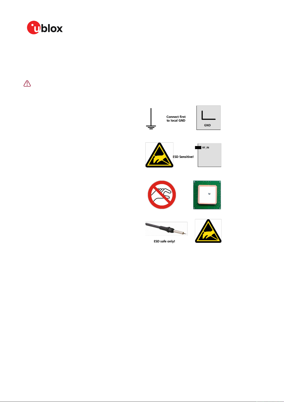
NEO-D9S-Integration manual
5 Product handling
5.1 ESD handling precautions
NEO-D9S contains highly sensitive electronic circuitry and is an Electrostatic Sensitive
Device (ESD). Observe precautions for handling! Failure to observe these precautions can
result in severe damage to the GNSS receiver!
•
Unless there is a galvanic coupling between the local
GND (i.e. the work table) and the PCB GND, then the first
point of contact when handling the PCB must always be
between the local GND and PCB GND.
•
Before mounting an antenna patch, connect ground of the
device.
•
When handling the RF pin, do not come into contact with
any charged capacitors and be careful when contacting
materials that can develop charges (e.g. patch antenna
~10 pF, coax cable ~50-80 pF/m or soldering iron).
•
To prevent electrostatic discharge through the RF input,
do not touch any exposed antenna area. If there is any risk
that such exposed antenna area is touched in non-ESD
protected work area, implement proper ESD protection
measures in the design.
•
When soldering RF connectors and patch antennas to the
receiver’s RF pin, make sure to use an ESD-safe soldering
iron (tip)
5.2 Soldering
Soldering paste
Use of “no clean” soldering paste is highly recommended, as it does not require cleaning after the
soldering process. The paste in the example below meets these criteria.
• Soldering paste: OM338 SAC405 / Nr.143714 (Cookson Electronics)
• Alloy specification: Sn 95.5/ Ag 4/ Cu 0.5 (95.5% tin/ 4% silver/ 0.5% copper)
• Melting temperature: 217 °C
• Stencil thickness: The exact geometry, distances, stencil thicknesses and solder paste
volumes must be adapted to the customer's specific production processes (e.g. soldering).
Reflow soldering
A convection-type soldering oven is highly recommended over the infrared-type radiation oven.
Convection-heated ovens allow precise control of the temperature, and all parts will heat up evenly,
regardless of material properties, thickness of components and surface color.
UBX-19026111 - R05
C1-Public Early production information
5 Product handling Page 41 of 51
Page 42

NEO-D9S-Integration manual
As a reference, see “IPC-7530 Guidelines for temperature profiling for mass soldering (reflow and
wave) processes”, published in 2001.
Preheat phase
During the initial heating of component leads and balls, residual humidity will be dried out. Note that
the preheat phase does not replace prior baking procedures.
• Temperature rise rate: max 3 °C/s. If the temperature rise is too rapid in the preheat phase,
excessive slumping may be caused
• Time: 60 – 120 s. If the preheat is insufficient, rather large solder balls tend to be generated.
Conversely, if performed excessively, fine balls and large balls will be generated in clusters
• End temperature: 150 – 200 °C. If the temperature is too low, non-melting tends to be caused in
areas containing large heat capacity
Heating - reflow phase
The temperature rises above the liquidus temperature of 217 °C. Avoid a sudden rise in temperature
as the slump of the paste could become worse.
• Limit time above 217 °C liquidus temperature: 40 – 60 s
• Peak reflow temperature: 245 °C
Cooling phase
A controlled cooling prevents negative metallurgical effects of the solder (solder becomes more
brittle) and possible mechanical tensions in the products. Controlled cooling helps to achieve bright
solder fillets with a good shape and low contact angle.
• Temperature fall rate: max 4 °C/s
To avoid falling off, the modules should be placed on the topside of the motherboard during
soldering.
The final soldering temperature chosen at the factory depends on additional external factors such
as the choice of soldering paste, size, thickness and properties of the base board, etc. Exceeding the
maximum soldering temperature in the recommended soldering profile may permanently damage
the module.
Figure 30: Soldering profile
UBX-19026111 - R05
C1-Public Early production information
5 Product handling Page 42 of 51
Page 43
NEO-D9S-Integration manual
Modules must not be soldered with a damp heat process.
Optical inspection
After soldering the module, consider optical inspection.
Cleaning
Do not clean with water, solvent, or ultrasonic cleaner:
• Cleaning with water will lead to capillary effects where water is absorbed into the gap between
the baseboard and the module. The combination of residues of soldering flux and encapsulated
water leads to short circuits or resistor-like interconnections between neighboring pads.
• Cleaning with alcohol or other organic solvents can result in soldering flux residues flowing
underneath the module, into areas that are not accessible for post-cleaning inspections. The
solvent will also damage the sticker and the printed text.
• Ultrasonic cleaning will permanently damage the module, in particular the quartz oscillators.
The best approach is to use a "no clean" soldering paste and eliminate the cleaning step after the
soldering.
Repeated reflow soldering
Repeated reflow soldering processes or soldering the module upside down are not
recommended.
A board that is populated with components on both sides may require more than one reflow
soldering cycle. In such a case, the process should ensure the module is only placed on the board
submitted for a single final upright reflow cycle. A module placed on the underside of the board may
detach during a reflow soldering cycle due to lack of adhesion.
The module can also tolerate an additional reflow cycle for re-work purposes.
Wave soldering
Base boards with combined through-hole technology (THT) components and surface-mount
technology (SMT) devices require wave soldering to solder the THT components. Only a single wave
soldering process is encouraged for boards populated with modules.
Rework
We do not recommend using a hot air gun because it is an uncontrolled process and can damage
the module.
Use of a hot air gun can lead to overheating and severely damage the module. Always avoid
overheating the module.
After the module is removed, clean the pads before re-applying solder paste, placing and reflow
soldering a new module.
Never attempt a rework on the module itself, e.g. by replacing individual components. Such
actions will immediately void the warranty.
Conformal coating
Certain applications employ a conformal coating of the PCB using HumiSeal® or other related
coating products. These materials affect the RF properties of the GNSS module and it is important
to prevent them from flowing into the module. The RF shields do not provide 100% protection for
the module from coating liquids with low viscosity. Apply the coating carefully.
Conformal coating of the module will void the warranty.
UBX-19026111 - R05
C1-Public Early production information
5 Product handling Page 43 of 51
Page 44

NEO-D9S-Integration manual
Casting
If casting is required, use viscose or another type of silicon pottant. The OEM is strongly advised to
qualify such processes in combination with the module before implementing this in the production.
Casting will void the warranty.
Grounding metal covers
Attempts to improve grounding by soldering ground cables, wick or other forms of metal strips
directly onto the EMI covers is done at the customer’s own risk. The numerous ground pins should
be sufficient to provide optimum immunity to interferences and noise.
u-blox makes no warranty for damages to the module caused by soldering metal cables or
any other forms of metal strips directly onto the EMI covers.
Use of ultrasonic processes
Some components on the module are sensitive to ultrasonic waves. Use of any ultrasonic processes
(cleaning, welding etc.) may cause damage to the GNSS receiver.
u-blox offers no warranty against damages to the module caused by ultrasonic processes.
5.3 Tapes
Figure 31 shows the feed direction and illustrates the orientation of the NEO-D9S on the tape:
Figure 31: Orientation of NEO-D9S on the tape
The dimensions of the tapes for NEO-D9S are specified in Figure 32 (measurements in mm).
UBX-19026111 - R05
C1-Public Early production information
5 Product handling Page 44 of 51
Page 45

NEO-D9S-Integration manual
Figure 32: NEO-D9S tape dimensions (mm)
5.4 Reels
The NEO-D9S receivers are deliverable in quantities of 250 pieces on a reel. The receivers are shipped
on reel type B, as specified in the u-blox Package Information Guide [5].
5.5 Moisture sensitivity levels
The moisture sensitivity level (MSL) for NEO-D9S is specified in the table below.
Package MSL level
LGA 4
Table 11: MSL level
For MSL standard see IPC/JEDEC J-STD-020, which can be downloaded from
www.jedec.org.
For more information regarding moisture sensitivity levels, labeling, storage and drying, see
the u-blox Package Information Guide [5].
UBX-19026111 - R05
C1-Public Early production information
5 Product handling Page 45 of 51
Page 46

NEO-D9S-Integration manual
Appendix
A Stacked patch antenna
A typical low cost L1 + L2 + L band antenna is based on a stacked patch antenna design. This
consists of two discrete ceramic patch elements with an L1/ L band patch above an L2 patch.
Figure 33: Ceramic stack
When used in an automotive application, the antenna placement can affect the phase center
variation owing to the size and shape of the ground plane coupled with the effects of the adjacent
structures. A phase center variation calibration is required to check the actual antenna position. A
successful calibration can be made if the phase variation of a specific antenna is repeatable between
samples.
To obtain the best antenna performance in an automotive application, mount the antenna in the
center of a conductive car roof without any inclination. The antenna requires good signal levels and
as wide a view of the sky as possible. The antenna must not be placed under a dashboard, in the rear
view mirror, or on the rear parcel shelf.
An L1 + L2 + L band stacked patch antenna must have a good band-pass performance from the
patch elements with low attenuation from SAW band-pass filtering. An example of the measured
frequency characteristics of a low-cost L1 + L2 + L band antenna is shown below.
UBX-19026111 - R05
C1-Public Early production information
Appendix Page 46 of 51
Page 47

NEO-D9S-Integration manual
Figure 34: Low cost L1/L2/L band antenna band characteristics
In the above test the L band antenna patch gain and pass band roll off is not to the required
specification and is included purely as an example.
B Glossary
Abbreviation Definition
ANSI American National Standards Institute
ARP Antenna reference point
BeiDou Chinese navigation satellite system
BBR Battery-backed RAM
CDMA Code-division multiple access
EMC Electromagnetic compatibility
EMI Electromagnetic interference
EOS Electrical overstress
EPA Electrostatic protective area
ESD Electrostatic discharge
Galileo European navigation satellite system
GLONASS Russian navigation satellite system
GND Ground
UBX-19026111 - R05
C1-Public Early production information
Appendix Page 47 of 51
Page 48

Abbreviation Definition
GNSS Global navigation satellite system
GPS Global Positioning System
GSM Global System for Mobile Communications
I2C Inter-integrated circuit bus
IEC International Electrotechnical Commission
PCB Printed circuit board
PMP Point to multipoint transmission
QZSS Quasi-Zenith Satellite System
RF Radio frequency
SV Space vehicle, a satellite
UBX u-blox
NEO-D9S-Integration manual
UBX-19026111 - R05
C1-Public Early production information
Appendix Page 48 of 51
Page 49

NEO-D9S-Integration manual
Related documents
[1] NEO-D9S Data sheet, UBX-18012996
[2] NEO-D9S Integration manual, UBX-19026111
[3] NEO-D9S Interface description, UBX-19048765
[4] u-blox ZED-F9P Integration manual, UBX-18010802
[5] Packaging information for u-blox chips, modules, and antennas, UBX-14001652
For regular updates to u-blox documentation and to receive product change notifications
please register on our homepage https://www.u-blox.com.
UBX-19026111 - R05
C1-Public Early production information
Related documents Page 49 of 51
Page 50

NEO-D9S-Integration manual
Revision history
Revision Date Name Status / comments
R01 04-July-2019 ghun Objective Specification
R02 17-Dec-2019 ghun/jhak Advance Information - V_BCKP pin connect to VCC. I2C, SPI, antenna
R03 04-Feb-2020 ghun Early production information - I2C address changed.
R04 19-Feb-2020 ghun Early production information - Tape dimension picture updated, missing
R05 13-Oct-2020 ghun/dama USB interface section update. Add C/N0 specification in antenna section.
supervisor, EXTINT, TX-READY, extended TX timeout, software back-up
mode added.
tape picture added.
Add C/N0 levels limits in production testing section
UBX-19026111 - R05
C1-Public Early production information
Revision history Page 50 of 51
Page 51

NEO-D9S-Integration manual
Contact
For complete contact information visit us at www.u-blox.com.
u-blox Offices
North, Central and South America Headquarters Asia, Australia, Pacific
u-blox America, Inc. u-blox AG u-blox Singapore Pte. Ltd.
Phone: +1 703 483 3180 Phone: +41 44 722 74 44 Phone: +65 6734 3811
E-mail: info_us@u-blox.com E-mail: info@u-blox.com E-mail: info_ap@u-blox.com
Support: support@u-blox.com Support: support_ap@u-blox.com
Regional Office West Coast Regional Office Australia
Phone: +1 408 573 3640 Phone: +61 2 8448 2016
E-mail: info_us@u-blox.com E-mail: info_anz@u-blox.com
Support: support_ap@u-blox.com
Technical Support Regional Office China (Beijing)
Phone: +1 703 483 3185 Phone: +86 10 68 133 545
E-mail: support_us@u-blox.com E-mail: info_cn@u-blox.com
Support: support_cn@u-blox.com
Regional Office China (Chongqing)
Phone: +86 23 6815 1588
E-mail: info_cn@u-blox.com
Support: support_cn@u-blox.com
Regional Office China (Shanghai)
Phone: +86 21 6090 4832
E-mail: info_cn@u-blox.com
Support: support_cn@u-blox.com
Regional Office China (Shenzhen)
Phone: +86 755 8627 1083
E-mail: info_cn@u-blox.com
Support: support_cn@u-blox.com
Regional Office India
Phone: +91 80 4050 9200
E-mail: info_in@u-blox.com
Support: support_in@u-blox.com
Regional Office Japan (Osaka)
Phone: +81 6 6941 3660
E-mail: info_jp@u-blox.com
Support: support_jp@u-blox.com
Regional Office Japan (Tokyo)
Phone: +81 3 5775 3850
E-mail: info_jp@u-blox.com
Support: support_jp@u-blox.com
Regional Office Korea
Phone: +82 2 542 0861
E-mail: info_kr@u-blox.com
Support: support_kr@u-blox.com
Regional Office Taiwan
Phone: +886 2 2657 1090
E-mail: info_tw@u-blox.com
Support: support_tw@u-blox.com
Europe, Middle East, Africa
UBX-19026111 - R05
C1-Public Early production information
Page 51 of 51
 Loading...