

Page 1
UBX-13004749 - R26
C1-Public www.u-blox.com
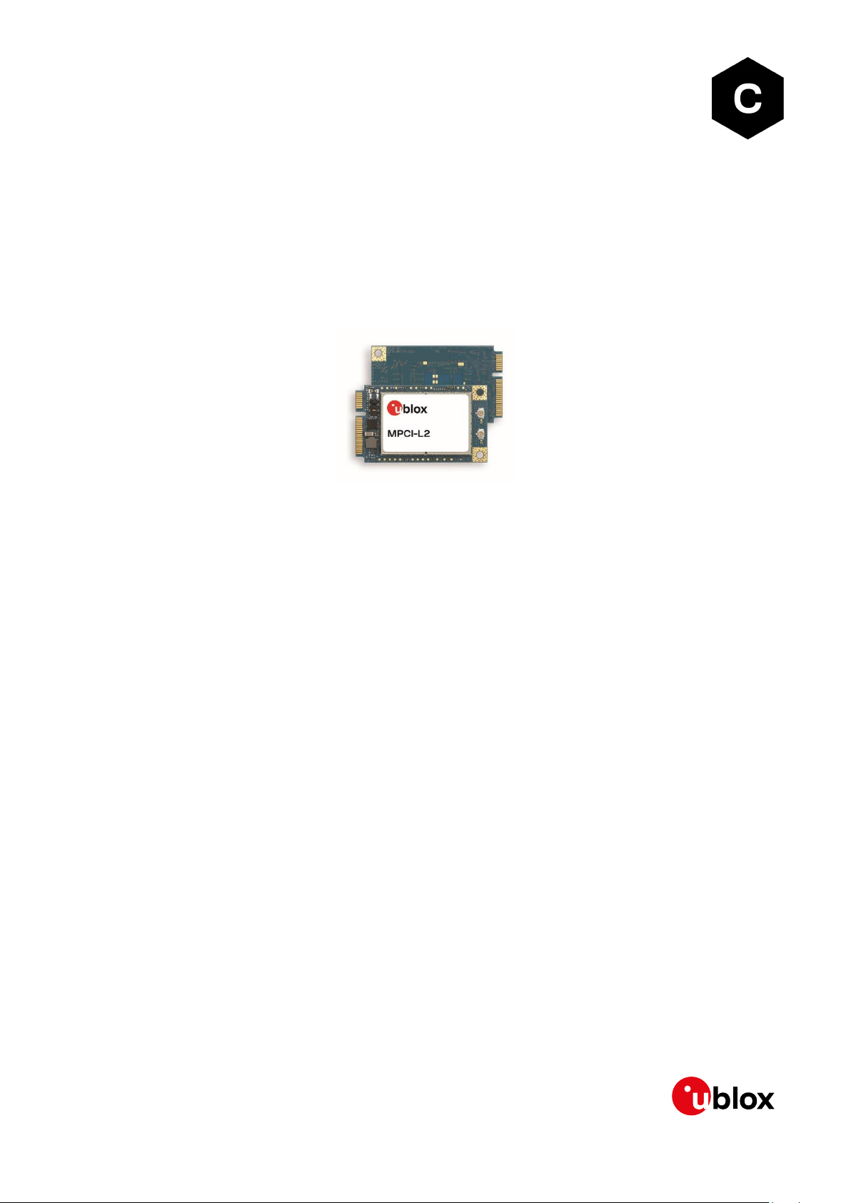
MPCI-L2 series
Multi-mode LTE Cat 4 Mini PCIe modules with HSPA+
and/or 2G fallback
Data sheet
Abstract
Technical data sheet describing MPCI-L2 series multi-mode cellular modules. The modules are a
complete and cost efficient LTE/3G/2G multi-mode solution offering up to 150 Mbit/s download data
rate and up to 50 Mbit/s upload data rate. The different variants offer a selection of coverage of up
to six LTE bands, up to five WCDMA/DC-HSPA+ bands and up to four GSM/EGPRS bands. The
modules have the industry standard PCI Express Mini Card form factor, which enables easy
integration into an application board and is also ideal for manufacturing of small series.
Page 2
MPCI-L2 series - Data sheet
UBX-13004749 - R26 Document information Page 2 of 31
C1-Public
Document information
Title
MPCI-L2 series
Subtitle
Multi-mode LTE Cat 4 Mini PCIe modules with HSPA+ and/or 2G fallback
Document type
Data sheet
Document number
UBX-13004749
Revision and date
R26
09-Dec-2020
Disclosure restriction
C1-Public
Product status
Corresponding content status
Functional Sample
Draft
For functional testing. Revised and supplementary data will be published later.
In development /
Prototype
Objective specification
Target values. Revised and supplementary data will be published later.
Engineering sample
Advance information
Data based on early testing. Revised and supplementary data will be published later.
Initial production
Early production information
Data from product verification. Revised and supplementary data may be published later.
Mass production /
End of life
Production information
Document contains the final product specification.
Page 3

MPCI-L2 series - Data sheet
UBX-13004749 - R26 Document information Page 3 of 31
C1-Public
This document applies to the following products:
Product name
Type number
Modem version
Application version
PCN reference
Product status
MPCI-L200
MPCI-L200-00S-00
09.71
A01.15
UBX-14044437
Obsolete
MPCI-L200-00S-01
09.71
A01.30
UBX-16026448
Obsolete
MPCI-L200-02S-00
15.90
A01.00
UBX-15029946
Obsolete
MPCI-L200-02S-01
15.90
A01.10
UBX-16031212
End of life
MPCI-L200-03S-00
15.90
A01.50
UBX-17022983
Obsolete
15.90
A01.52
UBX-19058317
Mass production
MPCI-L201
MPCI-L201-01S-00
09.93
A01.07
UBX-18012849
End of life
MPCI-L201-02S-00
09.93
For Verizon: 09.94
A02.50
For Verizon: A01.02
UBX-17013932
End of life
09.93
For Verizon: 10.04
A02.52
For Verizon: A01.01
UBX-19058317
End of life
MPCI-L201-02S-01
20.03
For Verizon: 20.03
A01.02
For Verizon: A01.02
UBX-19000820
End of life
20.03
For Verizon: 20.04
A01.04
For Verizon: A01.00
UBX-19058317
End of life
MPCI-L201-02S-02
20.06
A01.00
UBX-20036068
Mass production
MPCI-L210
MPCI-L210-00S-00
09.71
A01.15
UBX-14044437
Obsolete
MPCI-L210-02S-00
15.63
A01.03
UBX-15029946
Obsolete
MPCI-L210-02S-01
15.63
A01.10
UBX-16031212
Obsolete
MPCI-L210-03S-00
15.63
A01.50
UBX-17022983
End of life
15.63
A01.52
UBX-19058317
End of life
MPCI-L210-03S-01
16.19
A01.04
UBX-20027569
Mass production
MPCI-L210-60S-00
09.94
A01.00
UBX-15021694
Obsolete
MPCI-L210-60S-01
09.94
A01.01
UBX-19042394
End of life
09.94
A01.08
UBX-19058317
End of life
MPCI-L210-63S-00
09.94
A01.07
UBX-20009693
Mass production
MPCI-L220
MPCI-L220-02S-00
15.93
A01.00
UBX-16025501
Obsolete
15.93
A01.04
UBX-19058317
Mass production
MPCI-L220-62S-00
16.04
A01.00
UBX-17013073
Obsolete
16.04
A01.02
UBX-19058317
Mass production
MPCI-L280
MPCI-L280-02S-00
15.63
A01.03
UBX-15029946
Obsolete
MPCI-L280-02S-01
15.63
A01.10
UBX-16031212
End of life
MPCI-L280-03S-00
15.63
A01.50
UBX-17022983
Obsolete
15.63
A01.52
UBX-19058317
Mass production
u-blox or third parties may hold intellectual property rights in the products, names, logos and designs included in this document.
Copying, reproduction, modification or disclosure to third parties of this document or any part thereof is only permitted with the
express written permission of u-blox.
The information contained herein is provided “as is” and u-blox assumes no liability for its use. No warranty, either express or
implied, is given, including but not limited to, with respect to the accuracy, correctness, reliability and fitness for a particular
purpose of the information. This document may be revised by u-blox at any time without notice. For the most recent documents,
visit www.u-blox.com.
Copyright © u-blox AG.
Page 4

MPCI-L2 series - Data sheet
UBX-13004749 - R26 Contents Page 4 of 31
C1-Public
Contents
Document information ................................................................................................................................ 2
Contents .......................................................................................................................................................... 4
1 Functional description ......................................................................................................................... 6
1.1 Overview ........................................................................................................................................................ 6
1.2 Product features ......................................................................................................................................... 6
1.3 Block diagram .............................................................................................................................................. 7
1.4 Product description .................................................................................................................................... 7
1.5 AT command support ................................................................................................................................ 8
1.6 Supported features .................................................................................................................................... 9
2 Interfaces ................................................................................................................................................ 11
2.1 Module supply input .................................................................................................................................. 11
2.2 Antenna RF interfaces .............................................................................................................................. 11
2.3 System functions ....................................................................................................................................... 11
2.3.1 Module power-on ............................................................................................................................... 11
2.3.2 Module power-off ............................................................................................................................... 11
2.3.3 Module reset ....................................................................................................................................... 11
2.4 SIM interface ...............................................................................................................................................12
2.5 USB interface ..............................................................................................................................................12
2.6 W_DISABLE# .............................................................................................................................................. 13
2.7 LED_WWAN# ............................................................................................................................................. 13
3 Pin definition ......................................................................................................................................... 14
3.1 Pin assignment .......................................................................................................................................... 14
4 Electrical specifications .................................................................................................................... 16
4.1 Absolute maximum rating....................................................................................................................... 16
4.1.1 Maximum ESD ................................................................................................................................... 16
4.2 Operating conditions ................................................................................................................................. 17
4.2.1 Operating temperature range ......................................................................................................... 17
4.2.2 Current consumption ........................................................................................................................ 17
4.2.3 LTE/3G/2G RF characteristics ....................................................................................................... 18
4.2.4 Supply/power pins ............................................................................................................................ 18
4.2.5 USB pins ............................................................................................................................................. 18
4.2.6 SIM pins .............................................................................................................................................. 18
4.2.7 PERST# pin ........................................................................................................................................ 19
4.2.8 W_DISABLE# pin ............................................................................................................................... 19
4.2.9 LED_WWAN# pin .............................................................................................................................. 19
5 Mechanical specifications ............................................................................................................... 20
6 Qualification and approvals.............................................................................................................. 21
6.1 Reliability tests ...........................................................................................................................................21
6.2 Approvals .....................................................................................................................................................21
7 Product handling .................................................................................................................................. 22
7.1 Packaging ................................................................................................................................................... 22
7.2 ESD precautions ........................................................................................................................................ 22
Page 5

MPCI-L2 series - Data sheet
UBX-13004749 - R26 Contents Page 5 of 31
C1-Public
8 Default settings .................................................................................................................................. 23
9 Labeling and ordering information ............................................................................................... 24
9.1 Product labeling ......................................................................................................................................... 24
9.2 Explanation of codes ................................................................................................................................ 25
9.3 Ordering information ................................................................................................................................ 26
Appendix ........................................................................................................................................................ 27
Related documentation ............................................................................................................................29
Revision history .......................................................................................................................................... 30
Contact ........................................................................................................................................................... 31
Page 6

MPCI-L2 series - Data sheet
UBX-13004749 - R26 Functional description Page 6 of 31
C1-Public
1 Functional description
1.1 Overview
The MPCI-L2 series comprises complete and cost efficient LTE/3G/2G multi-mode cellular modules in
the industry standard PCI Express Mini Card form factor, which enables an easy integration into an
application board and it is also ideal for manufacturing of small series.
MPCI-L2modules support up to six LTE bands, up to five UMTS/DC-HSPA+ bands and up to four
GSM/(E)GPRS bands for data transmission over different regions and network operators.
With LTE Category 4 data rates of 150 Mb/s (downlink) and 50 Mb/s (uplink), the modules are ideal for
applications requiring the highest data-rates and high-speed internet access.
Typical applications are industrial computing, ruggedized terminals, video communications, wireless
routers, alarm panels and surveillance, digital signage and payment systems.
1.2 Product features
Model
LTE
UMTS
GSM
Interfaces
Audio
Features
Grade
LTE FDD category Bands HSDPA category HSUPA category Bands GNSS via modem (E)GPRS multi
-slot class
Bands UART
USB 2.0 SDIO (Master)
DDC (I
2C)
GPIOs Analog audio Digital audio Network indication Antenna supervisor MIMO 2x2 / Rx Diversity Remote SIM Access Profile
Embedded TCP/UDP stack Embedded HTTP, FTP FOTA
Dual stack IPv4/IPv6
Standard Professional Automotive
MPCI-L200
4
2,4,5
7,17
24
6
1,2,4
5,8
●
12
Quad
●
● ●
■ ■ ■
●
●
MPCI-L201
4
2,4,5
13,17
24 6 2,5 ● ● ● ● ● ● ● ● ●
MPCI-L210 1
4
1,3,5
7,8,20
24
6
1,2
5,8
●
12
Quad
● ● ● ■ ■ ■ ● ●
MPCI-L220 2
4
1,3,5
6,8,19
24
6
1,6
8,19
●
●
● ●
● ● ●
●
●
MPCI-L280
4
1,3,5
7,8,28
24
6
1,2
5,8
●
12
Quad
●
● ●
● ● ●
●
●
● = supported by all product versions ■ = supported by all product versions except versions “00”, “60”, “63"
Table 1: MPCI-L2 series main features summary
1
MPCI-L210-63S product version does not support LTE band 20
2
MPCI-L220-62S product version does not support UMTS Radio Access Technology
Page 7

MPCI-L2 series - Data sheet
UBX-13004749 - R26 Functional description Page 7 of 31
C1-Public
1.3 Block diagram
As described in Figure 1, each MPCI-L2 series module integrates one TOBY-L2 series module, which
represents the core of the device, providing the related LTE/3G/2G modem and processing
functionalities. Additional signal conditioning circuitry is implemented for PCI Express Mini Card
compliance, and two U.FL connectors are available for easy antennas integration.
ANT1
SIM
USB
W_DISABLE#
TOBY-L2
series
Signal
conditioning
ANT2
PERST#
LED_WWAN#
U.FL
U.FL
3.3Vaux (Supply)
Boost
converter
VCC
Figure 1: MPCI-L2 series block diagram
1.4 Product description
MPCI-L2 series modules provide 4G LTE, 3G WCDMA/DC-HSPA+, 2G GSM/(E)GPRS multi-mode
technology:
• MPCI-L200 and MPCI-L201 are mainly designed for operation in America
• MPCI-L210 is mainly designed for operation in Europe, Asia and other countries
• MPCI-L220 is mainly designed for operation in Japan
• MPCI-L280 is mainly designed for operation in south-east Asia and Oceania
4G LTE
3G UMTS/HSDPA/HSUPA
2G GSM/GPRS/EDGE
3GPP Release 9
Long Term Evolution (LTE)
Evolved UTRA (E-UTRA)
Frequency Division Duplex (FDD)
DL Multi-Input Multi-Output (MIMO) 2x2
3GPP Release 8
Dual-Cell HS Packet Access (DC-HSPA+)
UMTS Terrestrial Radio Access (UTRA)
Frequency Division Duplex (FDD)
DL Rx diversity
3GPP Release 8
Enhanced Data rate GSM Evolution (EDGE)
GSM EGPRS Radio Access (GERA)
Time Division Multiple Access (TDMA)
DL Advanced Rx Performance Phase 1
Band support 3:
• MPCI-L200:
• Band 17 (700 MHz)
• Band 5 (850 MHz)
• Band 4 (1700 MHz)
• Band 2 (1900 MHz)
• Band 7 (2600 MHz)
Band support:
• MPCI-L200:
• Band 5 (850 MHz)
• Band 8 (900 MHz)
• Band 4 (AWS, i.e. 1700 MHz)
• Band 2 (1900 MHz)
• Band 1 (2100 MHz)
Band support:
• MPCI-L200:
• GSM 850 MHz
• E-GSM 900 MHz
• DCS 1800 MHz
• PCS 1900 MHz
• MPCI-L201:
• Band 17 (700 MHz)
• Band 13 (750 MHz)
• Band 5 (850 MHz)
• Band 4 (1700 MHz)
• Band 2 (1900 MHz)
• MPCI-L201:
• Band 5 (850 MHz)
• Band 2 (1900 MHz)
3
MPCI-L2 series modules support all the E-UTRA channel bandwidths for each operating band as per 3GPP TS 36.521-1 [11].
Page 8

MPCI-L2 series - Data sheet
UBX-13004749 - R26 Functional description Page 8 of 31
C1-Public
4G LTE
3G UMTS/HSDPA/HSUPA
2G GSM/GPRS/EDGE
• MPCI-L210 4:
• Band 20 (800 MHz)
• Band 5 (850 MHz)
• Band 8 (900 MHz)
• Band 3 (1800 MHz)
• Band 1 (2100 MHz)
• Band 7 (2600 MHz)
• MPCI-L210:
• Band 5 (850 MHz)
• Band 8 (900 MHz)
• Band 2 (1900 MHz)
• Band 1 (2100 MHz)
• MPCI-L210:
• GSM 850 MHz
• E-GSM 900 MHz
• DCS 1800 MHz
• PCS 1900 MHz
• MPCI-L220:
• Band 19 (850 MHz)
• Band 6 (850 MHz)
• Band 5 (850 MHz)
• Band 8 (900 MHz)
• Band 3 (1800 MHz)
• Band 1 (2100 MHz)
• MPCI-L220 5:
• Band 19 (850 MHz)
• Band 6 (850 MHz)
• Band 8 (900 MHz)
• Band 1 (2100 MHz)
• MPCI-L280:
• Band 28 (750 MHz)
• Band 5 (850 MHz)
• Band 8 (900 MHz)
• Band 3 (1800 MHz)
• Band 1 (2100 MHz)
• Band 7 (2600 MHz)
• MPCI-L280:
• Band 5 (850 MHz)
• Band 8 (900 MHz)
• Band 2 (1900 MHz)
• Band 1 (2100 MHz)
• MPCI-L280:
• GSM 850 MHz
• E-GSM 900 MHz
• DCS 1800 MHz
• PCS 1900 MHz
LTE Power Class
• Class 3 (23 dBm)
for LTE mode
WCDMA/HSDPA/HSUPA Power Class
• Class 3 (24 dBm)
for UMTS/HSDPA/HSUPA mode
GSM/GPRS (GMSK) Power Class
• Class 4 (33 dBm) in GSM/E-GSM band
• Class 1 (30 dBm) in DCS/PCS band
EDGE (8-PSK) Power Class
• Class E2 (27 dBm) in GSM/E-GSM band
• Class E2 (26 dBm) in DCS/PCS band
Data rate
• LTE category 4:
up to 150 Mb/s DL, 50 Mb/s UL
Data rate
• MPCI-L200, MPCI-L201:
• HSDPA cat.14, up to 21 Mb/s DL6
• HSUPA cat.6, up to 5.6 Mb/s UL
• MPCI-L210, MPCI-L220, MPCI-L280:
• HSDPA cat.24, up to 42 Mb/s DL
• HSUPA cat.6, up to 5.6 Mb/s UL
Data rate 7
• GPRS multi-slot class 12 8,
CS1-CS4, up to 85.6 kb/s DL/UL
• EDGE multi-slot class 12 8,
MCS1-MCS9 up to 236.8 kb/s DL/UL
Table 2: MPCI-L2 series LTE, 3G and 2G characteristics
1.5 AT command support
The MPCI-L2 series modules support AT commands according to 3GPP standards TS 27.007 [1],
27.005 [2] and the u-blox AT command extension.
☞ For the complete list of all the supported AT commands and their syntax, see the u-blox AT
commands manual [3].
RIL (Radio Interface Layer) software for Android is available for MPCI-L2 series modules free of
charge. See the Android RIL source code application note [4] for the supported software deliveries and
more information.
4
MPCI-L210-63S product version does not support LTE band 20
5
MPCI-L220-62S product version does not support 3G Radio Access Technology
6
HSDPA category 24 capable
7
GPRS/EDGE multi-slot class determines the number of timeslots available for upload and download and thus the speed at
which data can be transmitted and received, with higher classes typically allowing faster data transfer rates.
8
GPRS/EDGE multi-slot class 12 implies a maximum of 4 slots in Down-Link and 4 slots in Up-Link, with 5 slots in total.
Page 9
MPCI-L2 series - Data sheet
UBX-13004749 - R26 Functional description Page 9 of 31
C1-Public
1.6 Supported features
Table 3 lists some of the main features supported by MPCI-L2 series modules. For more details, see
the TOBY-L2 / MPCI-L2 system integration manual [5] and u-blox AT commands manual [3].
Feature
Description
Network Indication
LED_WWAN# signal provides the Wireless Wide Area Network status indication as specified by the
PCI Express Mini Card electromechanical specification [9].
Embedded TCP and
UDP stack 9
Embedded TCP/IP and UDP/IP stack including the Direct Link mode for TCP and UDP sockets.
Sockets can be set in Direct Link mode to establish a transparent end to end communication with an
already connected TCP or UDP socket via serial interface.
FTP 9, FTPS 10
File Transfer Protocol as well as Secure File Transfer Protocol (SSL encryption of FTP control
channel) functionalities are supported via AT commands.
HTTP 9, HTTPS 10
Hyper-Text Transfer Protocol as well as Secure Hyper-Text Transfer Protocol (SSL encryption)
functionalities are supported via AT commands.
Embedded TLS 1.2 10
With the support of X.509 certificates, Embedded TLS 1.2 provides server and client authentication,
data encryption, data signature and enables TCP/IP applications communicate over a secured and
trusted connection.
The feature can be configured and enabled by +USECMNG and +USECPRF AT commands.
DNS 9
Support for DNS functionality.
Dual stack IPv4/IPv6
Both Internet Protocol version 4 and Internet Protocol version 6 are supported in parallel.
BIP 11
Bearer Independent Protocol for Over-the-Air SIM provisioning. The data transfer to/from the SIM
uses either an already active PDP context or a new PDP context established with the APN provided by
the SIM card.
Multiple PDP contexts
Up to 8 PDP contexts can be activated, and multi secondary PDP contexts be associated to a primary
PDP context
SMS via IMS 12
Allows SMS via embedded IP Multimedia Subsystem (IMS)
Firmware update Over
AT commands (FOAT)
Firmware module upgrade over AT command interface (USB).
The feature can be enabled and configured through the +UFWUPD AT command.
Firmware update Over
The Air (FOTA) 9
Firmware module update over the LTE/3G/2G air interface.
The feature can be enabled and configured through the +UFWINSTALL AT command.
LTE DL MIMO 2x2 and
3G DL Rx Diversity
Improved cellular link quality and reliability on all operating bands.
Smart Temperature
Supervisor 13
Constant monitoring of the module board temperature:
• Warning notification when the temperature approaches an upper or lower predefined threshold
• Shutdown notified and forced when the temperature value is outside the specified range (shutdown
suspended in case of an emergency call in progress)
The Smart Temperature Supervisor feature can be enabled and configured through the +USTS AT
command.
☞ The sensor measures board temperature, which can differ from ambient temperature.
Remote SIM Access
Profile (SAP)14
Allows access and use of a remote (U)SIM card instead of the local SIM card directly connected to the
module (U)SIM interface. The module acts as an SAP Client establishing a connection and
performing data exchange to a SAP Server directly connected to the remote SIM. The modules
provide a dedicated USB SAP channel and a dedicated multiplexer SAP channel over UART for
communication with the remote (U)SIM card.
The feature can be configured and enabled by +USAPMODE and + USAPIND AT commands.
9
Not supported by “00”, “60” and “63” product versions
10
Not supported by “00”, “01”, “60”, “63” and MPCI-L201-02S product versions.
11
Not supported by “00”, “60”, “63” product versions. Not supported by MPCI-L201-01S and MPCI-L201-02S-00 product versions
in AT&T configuration.
12
Not supported by “00”, “03”, “60”, “62”, “63”, MPCI-L200-02S, MPCI-L210-02S, MPCI-L220-02S and MPCI-L280-02S product
versions.
13
Not supported by “00”, “01”, “60” and “63” product versions.
14
Not supported by “00”, “01”, “02”, “60”, “62” and “63” product versions
Page 10

MPCI-L2 series - Data sheet
UBX-13004749 - R26 Functional description Page 10 of 31
C1-Public
Feature
Description
Power saving
The power saving configuration is by default disabled, but it can be configured using the +UPSV AT
command. When power saving is enabled, the module automatically enters the low power idle-mode
whenever possible, reducing current consumption.
During idle-mode, the module processor core runs with the internal RTC 32 kHz reference clock.
Fast Dormancy
The Fast Dormancy feature, defined in 3GPP Rel.8, allows reduction of current consumption and
network utilization during periods of data inactivity. It can be activated by +UFDAC and
+UDCONF=61 AT commands.
Radio Policy Manager
(RPM)15
The Radio Policy Manager (RPM) feature provides a more efficient access to the network, controlling
the number of network accesses per service type over a fixed amount of time. For more details on the
RPM feature see the GSMA IoT device connection efficiency guidelines [12].
The feature can be enabled through the +URPM and +URPMCONF AT commands.
Table 3: Some of the main features supported by MPCI-L2 series modules
15
Not supported by product versions "00", "02", "60", "62", "63" of MPCI -L2x0 modules, not supported by product version "01" of
MPCI -L201 modules, and not supported by product versions MPCI-L2x0-03S-00 and MPCI -L201-02S-00
Page 11

MPCI-L2 series - Data sheet
UBX-13004749 - R26 Interfaces Page 11 of 31
C1-Public
2 Interfaces
2.1 Module supply input
MPCI-L2 series modules must be supplied through the 3.3Vaux pins by a DC power supply. The voltage
must be stable, because during this operation the current drawn from 3.3Vaux can vary significantly,
based on the power consumption profile of the LTE/3G/2G systems (see the TOBY-L2 / MPCI-L2
system integration manual [5]).
2.2 Antenna RF interfaces
The modules have two RF interfaces over two standard U.FL connectors (Hirose U.FL-R-SMT) with a
characteristic impedance of 50 . The primary RF port (ANT1) supports both Tx and Rx, providing the
main antenna interface, while the secondary RF port (ANT2) supports Rx only for the LTE MIMO 2x2
and 3G Rx diversity configurations.
2.3 System functions
2.3.1 Module power-on
MPCI-L2 series can be switched on by:
• Rising edge on the 3.3Vaux pin to a valid voltage for module supply, i.e. applying module supply.
2.3.2 Module power-off
MPCI-L2 series can be properly switched off by:
• Sending the AT+CFUN=127 command (see the u-blox AT commands manual [3]) to configure the
module in the halt mode, and then removing the 3.3Vaux supply. In this way, the current parameter
settings are saved in the module’s non-volatile memory and a proper network detach is performed.
An abrupt under-voltage shutdown occurs on MPCI-L2 modules when the 3.3Vaux supply is suddenly
removed. If this is done without previously configuring the module in the halt mode, the storage of the
current parameter settings in the module’s non-volatile memory and the proper network detach are
not performed.
An over-temperature or an under-temperature shutdown occurs on MPCI-L2 modules when the
temperature measured within the cellular module reaches the dangerous area, if the optional Smart
Temperature Supervisor feature (not supported by the “00”, “01”, “60” and “63” product versions) is
enabled and configured by the AT+USTS command. For more details, see the TOBY-L2 / MPCI-L2
system integration manual [5] and the u-blox AT commands manual [3].
2.3.3 Module reset
MPCI-L2 series can be reset (rebooted) by:
• AT+CFUN command (see the u-blox AT commands manual [3]).
• AT+CPWROFF command (see the u-blox AT commands manual [3]): this behavior differs than
TOBY-L2 modules, where MPCI-L2 series modules will boot back up, rather than remain powered
off, due to the MPCI-L2 series module’s internal configuration.
In both cases, an “internal” or “software” reset of the module is executed: the current parameter
settings are saved in the module’s non-volatile memory and a proper network detach is performed.
An abrupt “external” or “hardware” reset of the module occurs when a low level is applied on the
PERST# pin (normally set high by an internal pull-up) for a valid time period (see section 4.2.7). The
Page 12

MPCI-L2 series - Data sheet
UBX-13004749 - R26 Interfaces Page 12 of 31
C1-Public
current parameter settings are not saved in the module’s non-volatile memory and a proper network
detach is not performed. PERST# line should be driven by open drain, open collector or contact switch.
2.4 SIM interface
A SIM card interface is provided on the UIM_PWR, UIM_DATA, UIM_CLK, UIM_RESET pins of the
system connector as well as on a micro-SIM (3FF) card holder solderable on the back side of the board:
the high-speed SIM/ME interface is implemented as well as the automatic detection of the required
SIM supporting voltage.
Both 1.8 V and 3 V SIM types are supported (1.8 V and 3 V ME). Activation and deactivation with
automatic voltage switch from 1.8 V to 3 V is implemented, according to ISO-IEC 7816-3 specifications.
The SIM driver supports the PPS procedure for baud-rate selection, according to the values proposed
by the SIM card/chip.
2.5 USB interface
MPCI-L2 series modules include a high-speed USB 2.0 compliant interface with maximum 480 Mb/s
data rate, representing the interface for any communication with an external host application
processor. The module itself acts as a USB device and can be connected to any USB host equipped
with compatible drivers.
The USB_D+ / USB_D- lines carry the USB serial bus data and signaling, providing all the
functionalities for the bus attachment, configuration, enumeration, suspension or remote wakeup
according to the Universal Serial Bus revision 2.0 specification [6].
MPCI-L2 series modules provide by default the following set of USB functions:
• CDC-ACM modem: AT commands interface is available over this modem COM port
• RNDIS network adapter: Ethernet-over-USB connection is available over this network adapter
The USB of MPCI-L2 series modules can be configured by the AT+UUSBCONF command to select
different sets of USB functions available in a mutually exclusive way. The configured USB profile can
thus consist of a specific set of functions with various capabilities and purposes, such as:
• CDC-ACM for AT commands and data
• CDC-ACM for remote SIM Access Profile (SAP)
16
• CDC-ACM for diagnostic
• RNDIS for Ethernet-over-USB
• CDC-ECM for Ethernet-over-USB
For more details regarding USB configurations and capabilities, see the TOBY-L2 / MPCI-L2 system
integration manual [5] and the u-blox AT commands manual [3], +UUSBCONF AT command.
USB drivers are available for the following operating system platforms:
• Windows Vista
• Windows 7
• Windows 8
• Windows 8.1
• Windows 10
• Windows Embedded CE 6.0
17
• Windows Embedded Compact 7
17
• Windows Embedded Compact 2013
17
MPCI-L2 series modules are compatible with standard Linux/Android USB kernel drivers.
16
Not supported by “00”, “01”, “02”, “60”, “62” and “63” product versions
17
For more details see the Windows Embedded OS USB driver installation application note [7]
Page 13

MPCI-L2 series - Data sheet
UBX-13004749 - R26 Interfaces Page 13 of 31
C1-Public
2.6 W_DISABLE#
MPCI-L2 series includes the W_DISABLE# active-low input signal to disable the radio operations as
specified by the PCI Express Mini Card electromechanical specification [9].
2.7 LED_WWAN#
MPCI-L2 series includes the LED_WWAN# active-low open drain output to provide the Wireless Wide
Area Network status indication as specified by the PCI Express Mini Card electromechanical
specification [9].
Page 14

MPCI-L2 series - Data sheet
UBX-13004749 - R26 Pin definition Page 14 of 31
C1-Public
3 Pin definition
3.1 Pin assignment
No
PCI Express Mini Card
E.M. Spec. Rev. 2.0
MPCI-L2
Voltage
domain
I/O
Description
Remarks
1
WAKE#
NC N/A Internally not connected
2
3.3Vaux
3.3Vaux
3.3Vaux
I
MPCI supply input
Connect to external 3.3 V supply.
See 4.2.4 for detailed electrical specs.
3
COEX1
NC N/A Internally not connected
4
GND
GND
GND
N/A
Ground
Connect to ground
5
COEX2
NC N/A Internally not connected
6
1.5V
NC N/A Internally not connected
7
CLKREQ#
NC N/A Internally not connected
8
UIM_PWR
UIM_PWR
SIM O SIM supply output
1.8 V or 3.0 V output according to the
SIM card/chip voltage type.
See 4.2.6 for detailed electrical specs.
9
GND
GND
GND
N/A
Ground
Connect to ground
10
UIM_DATA
UIM_DATA
SIM
I/O
SIM data
input/output
Internal 4.7 k pull-up to UIM_PWR.
See 4.2.6 for detailed electrical specs.
11
REFCLK-
NC N/A Internally not connected
12
UIM_CLK
UIM_CLK
SIM O SIM clock output
3.25 MHz output for SIM card/chip.
See 4.2.6 for detailed electrical specs.
13
REFCLK+
NC N/A Internally not connected
14
UIM_RESET
UIM_RESET
SIM O SIM reset output
Reset output for SIM card/chip.
See 4.2.6 for detailed electrical specs.
15
GND
GND
GND
N/A
Ground
Connect to ground
16
UIM_SPU
NC N/A Internally not connected
17
UIM_IC_DM
NC N/A Internally not connected
18
GND
GND
GND
N/A
Ground
Connect to ground
19
UIM_IC_DP
NC N/A Internally not connected
20
W_DISABLE1#
W_DISABLE#
I
Wireless disable
input
Internal 22 k pull-up to 3.3Vaux.
See 4.2.8 for detailed electrical specs.
21
GND
GND
GND
N/A
Ground
Connect to ground
22
PERST#
PERST#
I MPCI reset input
Internal 45 k active pull-up to 3.3 V.
See 4.2.7 for detailed electrical specs.
23
PERn0
NC N/A Internally not connected
24
3.3Vaux
3.3Vaux
3.3Vaux
I
MPCI supply input
Connect to external 3.3 V supply.
See 4.2.4 for detailed electrical specs.
25
PERp0
NC N/A Internally not connected
26
GND
GND
GND
N/A
Ground
Connect to ground
27
GND
GND
GND
N/A Connect to ground
28
1.5V
NC N/A Internally not connected
29
GND
GND
GND
N/A
Ground
Connect to ground
30
SMB_CLK
NC N/A Internally not connected
31
PETn0
NC N/A Internally not connected
32
SMB_DATA
NC N/A Internally not connected
33
PETp0
NC N/A Internally not connected
34
GND
GND
GND
N/A
Ground
Connect to ground
Page 15

MPCI-L2 series - Data sheet
UBX-13004749 - R26 Pin definition Page 15 of 31
C1-Public
No
PCI Express Mini Card
E.M. Spec. Rev. 2.0
MPCI-L2
Voltage
domain
I/O
Description
Remarks
35
GND
GND
GND
N/A
Ground
Connect to ground
36
USB_D-
USB_D-
USB
I/O
USB Data Line D-
90 nominal differential impedance.
Pull-up, pull-down and series resistors
as required by USB 2.0 specifications
[6] are part of the USB pin driver and
need not be provided externally.
See 4.2.4 for detailed electrical specs.
37
GND
GND
GND
N/A
Ground
Connect to ground
38
USB_D+
USB_D+
USB
I/O
USB Data Line D+
90 nominal differential impedance.
Pull-up, pull-down and series resistors
as required by USB 2.0 specifications
[6] are part of the USB pin driver and
need not be provided externally.
See 4.2.4 for detailed electrical specs.
39
3.3Vaux
3.3Vaux
3.3Vaux
I
MPCI supply input
Connect to external 3.3 V supply.
See 4.2.4 for detailed electrical specs.
40
GND
GND
GND
N/A
Ground
Connect to ground
41
3.3Vaux
3.3Vaux
3.3Vaux
I
MPCI supply input
Connect to external 3.3 V supply.
See 4.2.4 for detailed electrical specs.
42
LED_WWAN#
LED_WWAN#
O LED indicator output
Open drain active low output.
See 4.2.9 for detailed electrical specs.
43
GND
GND
GND
N/A
Ground
Connect to ground
44
LED_WLAN#
NC N/A Internally not connected
45
Reserved
NC N/A Internally not connected
46
LED_WPAN#
NC N/A Internally not connected
47
Reserved
NC N/A Internally not connected
48
1.5V
NC N/A Internally not connected
49
Reserved
NC N/A Internally not connected
50
GND
GND
GND
N/A
Ground
Connect to ground
51
W_DISABLE2#
NC N/A Internally not connected
52
3.3Vaux
3.3Vaux
3.3Vaux
I
MPCI supply input
Connect to external 3.3 V supply.
See 4.2.4 for detailed electrical specs.
Table 4: MPCI-L2 series system connector pin assignment
Page 16

MPCI-L2 series - Data sheet
UBX-13004749 - R26 Electrical specifications Page 16 of 31
C1-Public
4 Electrical specifications
⚠ Stressing the device above one or more of the ratings listed in the Absolute Maximum Rating
section may cause permanent damage. These are stress ratings only. Operating the module at
these or at any conditions other than those specified in the Operating Conditions sections
(chapter 4.1) of the specification should be avoided. Exposure to Absolute Maximum Rating
conditions for extended periods may affect device reliability.
☞ Operating condition ranges define those limits within which the functionality of the device is
guaranteed.
☞ Electrical characteristics are defined according to verification on a representative number of
samples or according to simulation.
☞ Application information is advisory only and does not form part of the specification.
4.1 Absolute maximum rating
☞ Limiting values given below are in accordance with Absolute Maximum Rating System (IEC 134).
Symbol
Description
Condition
Min.
Max.
Unit
3.3Vaux
Module supply voltage
Input DC voltage at 3.3Vaux pins
–0.3
6.3 V USB
USB D+/D- pins
Input DC voltage at USB interface pins
3.6 V SIM
SIM interface
Input DC voltage at SIM interface pins
–0.3
3.6 V PERST#
MPCI reset input
Input DC voltage at PERST# input pin
–0.3
5.0 V W_DISABLE#
Wireless disable input
Input DC voltage at W_DISABLE# input pin
–0.3
3.6 V LED_WWAN#
LED indicator output
Input DC voltage at LED_WWAN# output pin
–0.3
6.0 V Rho_ANT
Antenna ruggedness
Output RF load mismatch ruggedness at ANT1 / ANT2
10:1
VSWR
Tstg
Storage temperature
–40
85
°C
Table 5: Absolute maximum ratings
⚠ The product is not protected against overvoltage or reversed voltages. If necessary, voltage spikes
exceeding the power supply voltage specification, given in table above, must be limited to values
within the specified boundaries by using appropriate protection devices.
4.1.1 Maximum ESD
Parameter
Min
Typ
Max
Unit
Remarks
ESD sensitivity for all pins
except ANT1 / ANT2
1000
V
Human Body Model according to JESD22-A114
ESD sensitivity for ANT1 / ANT2
1000
V
Human Body Model according to JESD22-A114
ESD immunity for ANT1 / ANT2
4000
V
Contact Discharge according to IEC 61000-4-2
8000
V
Air Discharge according to IEC 61000-4-2
Table 6: Maximum ESD ratings
⚠ u-blox cellular modules are Electrostatic Sensitive Devices and require special precautions when
handling. See section 7.2 for ESD handling instructions.
Page 17
MPCI-L2 series - Data sheet
UBX-13004749 - R26 Electrical specifications Page 17 of 31
C1-Public
4.2 Operating conditions
☞ Unless otherwise indicated, all operating condition specifications are at an ambient temperature
of +25 °C.
⚠ Operation beyond the operating conditions is not recommended and extended exposure beyond
them may affect device reliability.
4.2.1 Operating temperature range
Parameter
Min.
Typical
Max.
Unit
Remarks
Normal operating temperature
–20
+25
+65
°C
Normal operating temperature range
(fully functional and meet 3GPP / ETSI specifications)
Extended operating temperature
–40 +85
°C
Extended operating temperature range
(RF performance may be affected outside normal
operating range, though module is fully functional)
Table 7: Environmental conditions
4.2.2 Current consumption
Mode
Condition
Tx power
Min
Typ
Max
Unit
Idle-Mode
(Power Saving enabled by AT+UPSV,
module in low power idle-mode,
equivalent to +CFUN=4 or +COPS=2)
Averaged current value over a 100-ms period,
USB connected and suspended
1.8 mA
Cyclic Idle/Active-Mode
(Power Saving enabled by AT+UPSV,
Module registered with network)
Averaged current value over a 10-minute period,
USB interface suspended
3.9 mA
Active-Mode
(Power Saving disabled by AT+UPSV,
Module registered with network)
Averaged current value over a 10-minute period,
USB interface not suspended
59 mA
2G Connected Mode
(Tx / Rx call enabled)
Pulse current during a 1-slot GMSK Tx burst,
850/900 MHz bands
Maximum
2.6 A
Averaged current value over a 10-second period,
2G GMSK call, 1 Tx + 1 Rx slot, 850/900 MHz
Maximum
380 mA
Averaged current value over a 10-second period,
2G GMSK call, 1 Tx + 1 Rx slot, 1800/1900 MHz
Maximum
295 mA
3G Connected Mode
(Tx / Rx call enabled)
Averaged current value over a 10-second period,
3G call with Low data rate
Minimum
245 mA
0 dBm
265 mA
12 dBm
365 mA
18 dBm
505 mA
Maximum
680 mA
Averaged current value over a 10-second period,
3G call with Maximum data rate
Maximum
)
790 mA
LTE Connected Mode
(Tx / Rx call enabled)
Averaged current value over a 10-second period,
LTE call with Low data rate
Minimum
395 mA
0 dBm
415 mA
12 dBm
520 mA
18 dBm
650 mA
Maximum
815 mA
Averaged current value over a 10-second period,
LTE call with Maximum data rate
Maximum
880 mA
Table 8: Module 3.3Vaux supply current consumption
Page 18

MPCI-L2 series - Data sheet
UBX-13004749 - R26 Electrical specifications Page 18 of 31
C1-Public
4.2.3 LTE/3G/2G RF characteristics
MPCI-L2 series LTE/3G/2G RF characteristics are specified in the TOBY-L2 series data sheet [10].
4.2.4 Supply/power pins
Symbol
Parameter
Min.
Typical
Max.
Unit
3.3Vaux
Module supply operating input voltage 18
3.00
3.30
3.60
V
Table 9: Input characteristics of Supply/Power pins
4.2.5 USB pins
USB data lines (USB_D+ / USB_D-) are compliant to the USB 2.0 high-speed specification. The values
in Table 10 are for information only. See the USB 2.0 specifications [6] for detailed electrical
characteristics.
Parameter
Min.
Typical
Max.
Unit
Remarks
High-speed squelch detection threshold
(input differential signal amplitude)
100 150
mV High speed disconnect detection threshold
(input differential signal amplitude)
525 625
mV
High-speed data signaling input
common mode voltage range
–50 500
mV
High-speed idle output level
–10 10
mV
High-speed data signaling output high level
360 440
mV
High-speed data signaling output low level
–10 10
mV Chirp J level (output differential voltage)
700 1100
mV
Chirp K level (output differential voltage)
–900
–500
mV
Table 10: USB pins characteristics
4.2.6 SIM pins
The SIM pins are a dedicated interface to the external SIM card/chip. The electrical characteristics
fulfill regulatory specification requirements. The values in Table 11 are for information only.
Parameter
Min.
Typical
Max.
Unit
Remarks
UIM_PWR supply output
1.76
1.80
1.85 V 1.8 V SIM type
2.84
2.90
2.94 V 3.0 V SIM type
Low-level input
–0.30
0.63 V 1.8 V SIM type
–0.30
0.80 V 3.0 V SIM type
High-level input
1.17 2.10 V 1.8 V SIM type
2.00 3.30 V 3.0 V SIM type
Low-level output
0.00
0.45 V 1.8 V SIM type, Max value at IOL = +2.0 mA
0.00
0.40 V 3.0 V SIM type, Max value at IOL = +2.0 mA
High-level output
1.35
1.80 V
1.8 V SIM type, Min value at IOH = –2.0 mA
2.60
2.90 V
3.0 V SIM type, Min value at IOH = –2.0 mA
Input / Output leakage current
–500
500
nA
0 V < V
IN
< 0.63 V or 1.17 V < V
IN
< 2.10 V
0 V < V
IN
< 0.80 V or 2.00 V < V
IN
< 3.30 V
Clock frequency on UIM_CLK
3.25 MHz
Internal pull-up on UIM_DATA
4.7
k
Internal pull-up to UIM_PWR supply
Table 11: SIM pins characteristics
18
Input voltage at 3.3Vaux must be above the normal operating range minimum limit to switch-on the module.
Page 19

MPCI-L2 series - Data sheet
UBX-13004749 - R26 Electrical specifications Page 19 of 31
C1-Public
4.2.7 PERST# pin
Pin Name
Parameter
Min.
Typical
Max.
Unit
Remarks
PERST#
Low-level input
0.00 1.10 V High-level input
2.60 3.70 V L-level input current
-82 µA
Pull-up resistance
35
45
k
Internal active pull-up to 3.3 V
PERST# low time
2.1 s Low time to reset the module
Table 12: PERST# pin characteristics
4.2.8 W_DISABLE# pin
Pin Name
Parameter
Min.
Typical
Max.
Unit
Remarks
W_DISABLE#
Low-level input
0.00 0.80 V High-level input
2.00 3.60 V
Pull-up resistance
22
k
Internal pull-up to 3.3Vaux
Table 13: W_DISABLE# pin characteristics
4.2.9 LED_WWAN# pin
Pin Name
Parameter
Min.
Typical
Max.
Unit
Remarks
LED_WWAN#
Low-level output
0.00
0.40 V Open-drain output
Max value at IOL = +9.0 mA
Table 14: LED_WWAN# pin characteristics
Page 20

MPCI-L2 series - Data sheet
UBX-13004749 - R26 Mechanical specifications Page 20 of 31
C1-Public
5 Mechanical specifications
MPCI-L2 series modules are fully compliant to the 52-pin PCI Express Full-Mini Card Type F2 form
factor, with top-side and bottom-side keep-out areas, with 50.95 mm nominal length, 30 mm nominal
width and all the other dimensions as defined by the PCI Express Mini Card electromechanical
specification [9] except for the card thickness (nominal value is 3.7 mm), as described in Figure 2.
MPCI-L2 series modules weight is about 9.7 g.
3.7 mm
30 mm
50.95 mm
Pin 52
Pin 2
Pin 1
Pin 51
ANT1
ANT2
Top
View
Bottom
View
Side
View
Hole
GND
Hole
GND
Hole
GND
Hole
GND
45.25 mm
19 mm
11 mm
Figure 2: MPCI-L2 series mechanical dimensions (top, side and bottom views)
☞ For further details regarding mechanical specifications, see the PCI Express Mini Card
electromechanical specification [9].
Page 21

MPCI-L2 series - Data sheet
UBX-13004749 - R26 Qualification and approvals Page 21 of 31
C1-Public
6 Qualification and approvals
6.1 Reliability tests
Tests for product family qualifications according to ISO 16750 “Road vehicles - Environmental
conditions and testing for electrical and electronic equipment”, and appropriate standards.
6.2 Approvals
MPCI-L2 series modules comply with the Directive 2011/65/EU of the European Parliament and the
Council on the Restriction of Use of certain Hazardous Substances in Electrical and Electronic
Equipment (EU RoHS 2) and its amendment Directive (EU) 2015/863 (EU RoHS 3).
MPCI-L2 series modules are RoHS 3 compliant.
No natural rubbers, hygroscopic materials, or materials containing asbestos are employed.
Table 15 summarizes the main Regulatory and Network Operator approvals for the MPCI-L2 modules.
Certification scheme
MPCI-L200
MPCI-L201
MPCI-L210
MPCI-L220
MPCI-L280
CE (European Conformity)
• • •
FCC (US Certification)
• • • •
FCC identification number
Contains FCC ID
XPYTOBYL200
Contains FCC ID
XPYTOBYL201
Contains FCC ID
XPYTOBYL210
Contains FCC ID
XPYTOBYL280
ISED (Canadian Certification)
• • • •
ISED certification number
Contains IC
8595A-TOBYL200
Contains IC
8595A-TOBYL201
Contains IC
8595A-TOBYL210
Contains IC
8595A-TOBYL280
ANATEL (Brazilian Certification)
• •
RCM (Australian Certification)
• •
NCC (Taiwanese Certification)
• •
GITEKI (Japanese Certification)
• •
NTT DoCoMo (Network Operator)
•
SoftBank (Network Operator)
•
AT&T (Network Operator)
•
Verizon (Network Operator)
•
Table 15: MPCI-L2 series main certification approvals summary
☞ The above listed certifications might not be available for all the different product type numbers.
Please contact the u-blox office or sales representative nearest you for the complete list of
certification approvals available for the selected ordering number.
Page 22

MPCI-L2 series - Data sheet
UBX-13004749 - R26 Product handling Page 22 of 31
C1-Public
7 Product handling
7.1 Packaging
MPCI-L2 modules are delivered as hermetically sealed trays of 16 pieces, 10 trays in 1 package
(160 units in total), to enable efficient production, production lot set-up and tear-down. For more
information about packaging, see the u-blox package information user guide [8].
Quantities of less than 160 pieces are also available. Contact u-blox for more information.
7.2 ESD precautions
⚠ MPCI-L2 series modules contain highly sensitive electronic circuitry and are Electrostatic
Sensitive Devices (ESD). Handling MPCI-L2 series modules without proper ESD protection may
destroy or damage them permanently.
MPCI-L2 series modules are Electrostatic Sensitive Devices (ESD) and require special ESD
precautions typically applied to ESD sensitive components.
Table 6 reports the maximum ESD ratings of the MPCI-L2 series modules.
Proper ESD handling and packaging procedures must be applied throughout the processing, handling
and operation of any application that incorporates MPCI-L2 series module.
ESD precautions should be implemented on the application board where the module is mounted, as
described in the TOBY-L2 / MPCI-L2 series system integration manual [5].
⚠ Failure to observe these recommendations can result in severe damage to the device!
Page 23

MPCI-L2 series - Data sheet
UBX-13004749 - R26 Default settings Page 23 of 31
C1-Public
8 Default settings
Item
AT Settings
Comments
USB interface
Enabled
MPCI-L2 series modules provide by default the following set of USB functions:
• CDC-ACM for AT command and data
• RNDIS for Ethernet-over-USB connection
The USB can be configured by the AT+UUSBCONF command to select different
sets of USB functions available in mutually exclusive way, configuring the active
USB profile consisting of a specific set of functions with various capabilities and
purposes (for more details, see the TOBY-L2 / MPCI-L2 system integration
manual [5] and u-blox AT commands manual [3], +UUSBCONF AT command).
Power Saving
AT+UPSV=0
Disabled
Network registration
AT+COPS=0
Self network registration
Table 16: Default settings
Page 24

MPCI-L2 series - Data sheet
UBX-13004749 - R26 Labeling and ordering information Page 24 of 31
C1-Public
9 Labeling and ordering information
9.1 Product labeling
The labels of MPCI-L2 series modules include important product information as described in this
section.
Figure 3, Figure 4 and Figure 5 illustrate the label of MPCI-L2 series modules, which is placed on the
bottom side of the modules, including: the u-blox logo, Pb-free marking, product type number,
production lot, certification numbers and production country.
xxS-xx
Figure 3: Label of MPCI-L2 series modules (except MPCI-L210-60S, MPCI-L210-63S and MPCI-L220)
MPCI-L210
60S-xx
D150057003
003-150063
Figure 4: Label of MPCI-L210-60S and MPCI-L210-63S modules
MPCI-L220
xxS-xx
AD160009003
003-160020
Figure 5: Label of MPCI-L220 modules
Page 25

MPCI-L2 series - Data sheet
UBX-13004749 - R26 Labeling and ordering information Page 25 of 31
C1-Public
9.2 Explanation of codes
Three different product code formats are used. The Product Name is used in documentation such as
this data sheet and identifies all u-blox products, independent of packaging and quality grade. The
Ordering Code includes options and quality, while the Type Number includes the hardware and
firmware versions. Table 17 details these 3 different formats:
Format
Structure
Product Name
MPCI-TGVV
Ordering Code
MPCI-TGVV-MMQ
Type Number
MPCI-TGVV-MMQ-XX
Table 17: Product code formats
Table 18 explains the parts of the product code.
Code
Meaning
Example
PPPP
Form factor
MPCI
TG
Platform (Technology and Generation)
• Dominant technology: G: GSM; U: HSUPA; C: CDMA 1xRTT; N: NB-IoT;
R: LTE low data rate (Cat 1 and below); L: LTE high data rate (Cat 3 and above)
• Generation: 1…9
L2
VV
Variant function set based on the same platform [00…99]
00
MM
Major product version [00…99]
00
Q
Product grade
• S = professional
• A = automotive
S
XX
Minor product version (not relevant for certification)
Default value is 00
Table 18: Part identification code
Page 26

MPCI-L2 series - Data sheet
UBX-13004749 - R26 Labeling and ordering information Page 26 of 31
C1-Public
9.3 Ordering information
Ordering No.
Product
MPCI-L200-00S
LTE bands 2 / 4 / 5 / 7 / 17, DC-HSPA+ bands 1 / 2 / 4 / 5 / 8, (E)GPRS band 850 / 900 / 1800 / 1900,
PCI Express Mini Card module mainly designed for operation in America
51 x 30 x 3.7 mm, 160 pcs/package
MPCI-L200-02S
LTE bands 2 / 4 / 5 / 7 / 17, DC-HSPA+ bands 1 / 2 / 4 / 5 / 8, (E)GPRS band 850 / 900 / 1800 / 1900,
PCI Express Mini Card module mainly designed for operation in America,
supporting embedded TCP/UDP, HTTP/FTP, TLS/SSL, smart temperature supervisor
51 x 30 x 3.7 mm, 160 pcs/package
MPCI-L200-03S
LTE bands 2 / 4 / 5 / 7 / 17, DC-HSPA+ bands 1 / 2 / 4 / 5 / 8, (E)GPRS band 850 / 900 / 1800 / 1900,
PCI Express Mini Card module mainly designed for operation in America,
supporting embedded TCP/UDP, HTTP/FTP, TLS/SSL, smart temperature supervisor, SAP
51 x 30 x 3.7 mm, 160 pcs/package
MPCI-L201-01S
LTE bands 2 / 4 / 5 / 13 / 17, DC-HSPA+ bands 1 / 2 / 5 / 8, (E)GPRS band 850 / 900 / 1800 / 1900,
PCI Express Mini Card module mainly designed for operation in America,
supporting embedded TCP/UDP, HTTP/FTP
51 x 30 x 3.7 mm, 160 pcs/package
MPCI-L201-02S
LTE bands 2 / 4 / 5 / 13 / 17, DC-HSPA+ bands 1 / 2 / 5 / 8, (E)GPRS band 850 / 900 / 1800 / 1900,
PCI Express Mini Card module mainly designed for operation in America,
supporting embedded TCP/UDP, HTTP/FTP, smart temperature supervisor
51 x 30 x 3.7 mm, 160 pcs/package
MPCI-L210-00S
LTE bands 1 / 3 / 5 / 7 / 8 / 20, DC-HSPA+ bands 1 / 2 / 5 / 8, (E)GPRS band 850 / 900 / 1800 / 1900,
PCI Express Mini Card module mainly designed for operation in Europe, Asia and other countries
51 x 30 x 3.7 mm, 160 pcs/package
MPCI-L210-60S
LTE bands 1 / 3 / 5 / 7 / 8 / 20, DC-HSPA+ bands 1 / 2 / 5 / 8, (E)GPRS band 850 / 900 / 1800 / 1900,
PCI Express Mini Card module approved by SoftBank Japanese mobile network operator
51 x 30 x 3.7 mm, 160 pcs/package
MPCI-L210-63S
LTE bands 1 / 3 / 5 / 7 / 8, DC-HSPA+ bands 1 / 2 / 5 / 8, (E)GPRS band 850 / 900 / 1800 / 1900,
PCI Express Mini Card module approved by SoftBank Japanese mobile network operator
51 x 30 x 3.7 mm, 160 pcs/package
MPCI-L210-02S
LTE bands 1 / 3 / 5 / 7 / 8 / 20, DC-HSPA+ bands 1 / 2 / 5 / 8, (E)GPRS band 850 / 900 / 1800 / 1900,
PCI Express Mini Card module mainly designed for operation in Europe, Asia and other countries,
supporting embedded TCP/UDP, HTTP/FTP, TLS/SSL, smart temperature supervisor
51 x 30 x 3.7 mm, 160 pcs/package
MPCI-L210-03S
LTE bands 1 / 3 / 5 / 7 / 8 / 20, DC-HSPA+ bands 1 / 2 / 5 / 8, (E)GPRS band 850 / 900 / 1800 / 1900,
PCI Express Mini Card module mainly designed for operation in Europe, Asia and other countries,
supporting embedded TCP/UDP, HTTP/FTP, TLS/SSL, smart temperature supervisor, SAP
51 x 30 x 3.7 mm, 160 pcs/package
MPCI-L220-02S
LTE bands 1 / 3 / 5 / 6 / 8 / 19, DC-HSPA+ bands 1 / 6 / 8 / 19,
PCI Express Mini Card module mainly designed for operation in Japan,
supporting embedded TCP/UDP, HTTP/FTP, TLS/SSL, smart temperature supervisor
51 x 30 x 3.7 mm, 160 pcs/package
MPCI-L220-62S
LTE bands 1 / 3 / 5 / 6 / 8 / 19,
PCI Express Mini Card module approved by NTT DoCoMo Japanese mobile network operator,
supporting embedded TCP/UDP, HTTP/FTP, TLS/SSL, smart temperature supervisor
51 x 30 x 3.7 mm, 160 pcs/package
MPCI-L280-02S
LTE bands 1 / 3 / 5 / 7 / 8 / 28, DC-HSPA+ bands 1 / 2 / 5 / 8, (E)GPRS bands 850 / 900 / 1800 / 1900,
PCI Express Mini Card module mainly designed for operation in South East-Asia and Oceania,
supporting embedded TCP/UDP, HTTP/FTP, TLS/SSL, smart temperature supervisor
51 x 30 x 3.7 mm, 160 pcs/package
MPCI-L280-03S
LTE bands 1 / 3 / 5 / 7 / 8 / 28, DC-HSPA+ bands 1 / 2 / 5 / 8, (E)GPRS bands 850 / 900 / 1800 / 1900,
PCI Express Mini Card module mainly designed for operation in South East-Asia and Oceania,
supporting embedded TCP/UDP, HTTP/FTP, TLS/SSL, smart temperature supervisor, SAP
51 x 30 x 3.7 mm, 160 pcs/package
Table 19: Product ordering codes
Page 27

MPCI-L2 series - Data sheet
UBX-13004749 - R26 Appendix Page 27 of 31
C1-Public
Appendix
A Glossary
Abbreviation
Definition
ANATEL
Agência Nacional de Telecomunicações (Brazilian National Telecommunications Agency)
AT
Hayes ATtention Command Set
BIP
Bearer Independent Protocol
CBS
Cell Broadcast Services
CDC
Communication Device Class
CDMA
Code-Division Multiple Access
CE
Certification Mark for compliance in the European Union
CLK
Clock
DC
Direct Current
DCE
Data Communication Equipment
DCS
Digital Cellular System
DDC
Display Data Channel
DL
Down Link (Reception)
DTE
Data Terminal Equipment
EDGE
Enhanced Data rates for GSM Evolution
EGPRS
Enhanced General Packet Radio Service
EOL
End of Life
ESD
Electrostatic Discharge
FCC
Federal Communications Commission
FDD
Frequency Division Duplex
FOAT
Firmware (update) Over AT commands
FOTA
Firmware (update) Over-The-Air
FTP
File Transfer Protocol
GERA
GSM EGPRS Radio Access
GITEKI
Gijutsu kijun tekigō shōmei - Japan technical standard conformity certification
GMSK
Gaussian Minimum-Shift Keying modulation
GND
Ground
GNSS
Global Navigation Satellite System
GPRS
General Packet Radio Services
GSM
Global System for Mobile communications
HSDPA
High Speed Downlink Packet Access
HSPA
High Speed Packet Access
HSUPA
High Speed Uplink Packet Access
HTTP
HyperText Transfer Protocol
I/O
Input/Output
I2C
Inter-Integrated Circuit
IC
Integrated Circuit
IEC
International Electrotechnical Commission
IMS
IP Multimedia System
IP
Internet Protocol
ISED
Innovation, Science and Economic Development, formerly known as Industry Canada (IC)
Page 28

MPCI-L2 series - Data sheet
UBX-13004749 - R26 Appendix Page 28 of 31
C1-Public
Abbreviation
Definition
ISO
International Organization for Standardization
LED
Light Emitting Diode
LTE
Long-Term Evolution
ME
Mobile Equipment
MIMO
Multiple In Multiple Out
N/A
Not Applicable
NCC
National Communications Commission
PCN
Product Change Notification
PPS
Protocol and Parameter Selection
RCM
Regulatory Compliance Mark
RF
Radio Frequency
RIL
Radio Interface Layer
RNDIS
Remote Network Driver Interface Specification
RTC
Real Time Clock
SAP
SIM Access Profile
SDIO
Secure Digital Input Output
SIM
Subscriber Identity Module
SMS
Short Message Service
SMT
Surface-Mount Technology
SSL
Secure Sockets Layer
TCP
Transmission Control Protocol
TCP/IP
Transmission Control Protocol/Internet Protocol
TDMA
Time-Division Multiple Access
TLS
Transport Layer Security
TS
Technical Specification
UART
Universal Asynchronous Receiver/Transmitter
UDP
User Datagram Protocol
UE
User Equipment
UL
Uplink (Transmission)
UMTS
Universal Mobile Telecommunications System
USB
Universal Serial Bus
VSWR
Voltage Standing Wave Ratio
WLAN
Wireless Local Area Network (IEEE 802.11 short range radio technology)
WWAN
Wireless Wide Area Network (GSM / UMTS / LTE cellular radio technology)
Table 20: Explanation of the abbreviations and terms used
Page 29

MPCI-L2 series - Data sheet
UBX-13004749 - R26 Related documentation Page 29 of 31
C1-Public
Related documentation
[1] 3GPP TS 27.007 - AT command set for User Equipment (UE)
[2] 3GPP TS 27.005 - Use of Data Terminal Equipment - Data Circuit terminating Equipment (DTE
- DCE) interface for Short Message Service (SMS) and Cell Broadcast Service (CBS)
[3] u-blox AT commands manual, UBX-13002752
[4] u-blox Android RIL source code application note, UBX-13002041
[5] u-blox TOBY-L2 / MPCI-L2 series system integration manual, UBX-13004618
[6] Universal Serial Bus revision 2.0 specification, https://www.usb.org/
[7] u-blox Windows Embedded OS USB driver installation application note, UBX-14003263
[8] u-blox package information user guide, UBX-14001652
[9] PCI Express Mini Card Electromechanical Specification, revision 2.0, April 21, 2012
[10] u-blox TOBY-L2 series data sheet, UBX-13004573
[11] 3GPP TS 36.521-1 - Evolved Universal Terrestrial Radio Access; User Equipment conformance
specification; radio transmission and reception; part 1: conformance testing
[12] GSMA TS.34 - IoT device connection efficiency guidelines
☞ For regular updates to u-blox documentation and to receive product change notifications, register
on our homepage (www.u-blox.com).
Page 30

MPCI-L2 series - Data sheet
UBX-13004749 - R26 Revision history Page 30 of 31
C1-Public
Revision history
Revision
Date
Name
Status / Comments
R01
20-Dec-2013
jpod / sses
Initial release
R02
14-Oct-2014
lpah / sses
Advance Information document status; Updated module power-on, power-off
and reset description; Updated module thickness and improved mechanical
description; Minor corrections in PERST#, W_DISABLE#, LED_WWAN#
description; Added module current consumption values; Added and updated
other minor electrical characteristics
R03
28-Jan-2015
sses
Early Production Information document status
R04
19-Aug-2015
sses
Objective Specification document status; Added description of MPCI-L200-02S,
MPCI-L210-02S and MPCI-L210-60S versions.
R05
25-Sep-2015
lpah
Advance Information status
R06
14-Oct-2015
sses
Objective Specification doc status; added description of MPCI-L280-02S version
R07
26-Nov-2015
lpah
Document status changed to Early Production Information
R08
22-Dec-2015
lpah / sses
Added description of MPCI-L201-01S version
R09
31-Mar-2016
sses
Updated features planned for future product versions.
Minor other corrections and description improvements.
R10
27-Apr-2016
lpah
Extended document applicability to MPCI-L210-60S-01
R11
15-Jul-2016
sses
Document status reverted to Objective Specification
Added description of MPCI-L201-02S version
R12
28-Sep-2016
sses
Document status updated to Advance Information
Updated support of some minor features in specific product versions
R13
21-Oct-2016
lpah
Document status updated to Early Production Information.
Extended document applicability to MPCI-L220-02S and MPCI-L280-72S
R14
25-Nov-2016
lpah
Extended document applicability to MPCI-L200-00S-01 and removed document
applicability to MPCI-L280-72S
R15
19-Apr-2017
lpah
"Disclosure restriction" replaces "Document status" on page 2 and doc footer.
Extended document applicability to the MPCI-L200-02S-01, MPCI-L210-02S-01,
MPCI-L220-62S and MPCI-L280-02S-01
R16
06-Jun-2017
lpah / sses
Updated MPCI-L201-02S product status to Intial Production
R17
23-Jun-2017
lpah / sses
Extended document applicability to the MPCI-L200-03S, MPCI-L210-03S and
MPCI-L280-03S
R18
27-Jul-2017
lpah
Updated MPCI-L200-00S-01, MPCI-L210-00S-00 product status to End of Life
R19
03-Jan-2018
lpah / sses
Updated MPCI-L200-02S-01, MPCI-L210-02S-01, MPCI-L280-02S-01 product
status to EOL. Updated absolute maximum rating of PERST# pin
R20
27-May-2018
lpah
Updated MPCI-L201-01S product status
Packaging information (section 7.1) updated, Reformat
R21
14-Feb-2019
lpah / sses
Extended document applicability to MPCI-L201-02S-01.
Updated packaging info (section 7.1) and the number of pieces for package
Updated approvals info; minor other corrections and description improvements
R22
12-Apr-2019
lpah / sses
Updated MPCI-L201-02S-01 product status. Updated RoHS statement.
R23
31-Oct-2019
lpah
Updated MPCI-L210-60S-01 product status.
Extended document applicability to MPCI-L210-63S product version.
R24
06-Apr-2020
lpah / sses
Updated MPCI-L210-63S product status.
R25
28-Aug-2020
lpah / sses
Extended document applicability to MPCI-L210-03S-01.
R26
09-Dec-2020
lpah / sses
Extended document applicability to MPCI-L201-02S-02.
Page 31

MPCI-L2 series - Data sheet
UBX-13004749 - R26 Contact Page 31 of 31
C1-Public
Contact
For complete contact information, visit us at www.u-blox.com.
u-blox Offices
North, Central and South America
u-blox America, Inc.
Phone: +1 703 483 3180
E-mail: info_us@u-blox.com
Regional Office West Coast:
Phone: +1 408 573 3640
E-mail: info_us@u-blox.com
Technical Support:
Phone: +1 703 483 3185
E-mail: support@u-blox.com
Headquarters
Europe, Middle East, Africa
u-blox AG
Phone: +41 44 722 74 44
E-mail: info@u-blox.com
Support: support@u-blox.com
Asia, Australia, Pacific
u-blox Singapore Pte. Ltd.
Phone: +65 6734 3811
E-mail: info_ap@u-blox.com
Support: support_ap@u-blox.com
Regional Office Australia:
Phone: +61 3 9566 7255
E-mail: info_anz@u-blox.com
Support: support_ap@u-blox.com
Regional Office China (Beijing):
Phone: +86 10 68 133 545
E-mail: info_cn@u-blox.com
Support: support_cn@u-blox.com
Regional Office China (Chongqing):
Phone: +86 23 6815 1588
E-mail: info_cn@u-blox.com
Support: support_cn@u-blox.com
Regional Office China (Shanghai):
Phone: +86 21 6090 4832
E-mail: info_cn@u-blox.com
Support: support_cn@u-blox.com
Regional Office China (Shenzhen):
Phone: +86 755 8627 1083
E-mail: info_cn@u-blox.com
Support: support_cn@u-blox.com
Regional Office India:
Phone: +91 80 405 092 00
E-mail: info_in@u-blox.com
Support: support_in@u-blox.com
Regional Office Japan (Osaka):
Phone: +81 6 6941 3660
E-mail: info_jp@u-blox.com
Support: support_jp@u-blox.com
Regional Office Japan (Tokyo):
Phone: +81 3 5775 3850
E-mail: info_jp@u-blox.com
Support: support_jp@u-blox.com
Regional Office Korea:
Phone: +82 2 542 0861
E-mail: info_kr@u-blox.com
Support: support_kr@u-blox.com
Regional Office Taiwan:
Phone: +886 2 2657 1090
E-mail: info_tw@u-blox.com
Support: support_tw@u-blox.com
 Loading...