

Page 1
LISA-U2 series
3.75G HSPA / HSPA+ Cellular Modules
System Integration Manual
Abstract
This document describes the features and the system integration of
LISA-U2 series HSPA+ cellular modules.
These modules are complete and cost efficient 3.75G solutions
offering up to six-band HSDPA/HSUPA and quad-band GSM/EGPRS
voice and/or data transmission technology in a compact form factor.
www.u-blox.com
UBX-13001118 - R19
Page 2
LISA-U2 series - System Integration Manual
UBX-13001118 - R19
Page 2 of 175
Document Information
Title
LISA-U2 series
Subtitle
3.75G HSPA / HSPA+ Cellular Modules
Document type
System Integration Manual
Document number
UBX-13001118
Revision, date
R19
09-Sep-2015
Document status
Early Production Information
Document status explanation
Objective Specification
Document contains target values. Revised and supplementary data will be published later.
Advance Information
Document contains data based on early testing. Revised and supplementary data will be published later.
Early Production Information
Document contains data from product verification. Revised and supplementary data may be published later.
Production Information
Document contains the final product specification.
This document applies to the following products:
Product name
Type number
Modem version
Application version
PCN / IN
LISA-U200
LISA-U200-01S-00
22.40 UBX-TN-12040
LISA-U200-02S-00
22.90 UBX-13003492
LISA-U200-03S-00
23.41
A01.01
UBX-15020745
LISA-U200-52S-00
22.86 UBX-13004628
LISA-U200-62S-00
22.90 UBX-13003492
LISA-U200 FOTA
LISA-U200-82S-00
22.92 UBX-13004629
LISA-U200-83S-00
23.41
A01.01
UBX-15020745
LISA-U201
LISA-U201-03S-00
23.41
A01.01
UBX-15020745
LISA-U230
LISA-U230-01S-00
22.40 UBX-TN-12040
LISA-U260
LISA-U260-01S-00
22.61 UBX-TN-12061
LISA-U260-02S-00
22.90 UBX-13003492
LISA-U270
LISA-U270-01S-00
22.61 UBX-TN-12061
LISA-U270-02S-00
22.90 UBX-13003492
LISA-U270-62S-00
22.90 UBX-13003492
LISA-U270-68S-00
22.93
A01.03
UBX-15019240
u-blox reserves all rights to this document and the information contained herein. Products, names, logos and designs described herein may in
whole or in part be subject to intellectual property rights. Reproduction, use, modification or disclosure to third parties of this document or
any part thereof without the express permission of u-blox is strictly prohibited.
The information contained herein is provided “as is” and u-blox assumes no liability for the use of the information. No warranty, either
express or implied, is given, including but not limited, with respect to the accuracy, correctness, reliability and fitness for a particular purpose
of the information. This document may be revised by u-blox at any time. For most recent documents, visit www.u-blox.com.
Copyright © 2015, u-blox AG.
u-blox® is a registered trademark of u-blox Holding AG in the EU and other countries. ARM® is the registered trademark of ARM Limited in
the EU and other countries.
Page 3

LISA-U2 series - System Integration Manual
UBX-13001118 - R19 Early Production Information Preface
Page 3 of 175
Preface
How to use this Manual
The LISA-U2 series System Integration Manual provides the necessary information to successfully design in and
configure these u-blox cellular modules.
This manual has a modular structure. It is not necessary to read it from the beginning to the end.
The following symbols are used to highlight important information within the manual:
An index finger points out key information pertaining to module integration and performance.
A warning symbol indicates actions that could negatively impact or damage the module.
u-blox Technical Documentation
As part of our commitment to customer support, u-blox maintains an extensive volume of technical
documentation for our products. In addition to our product-specific technical data sheets, the following manuals
are available to assist u-blox customers in product design and development.
AT Commands Manual: This document provides the description of the supported AT commands by the
LISA-U2 modules to verify all implemented functionalities.
System Integration Manual: This Manual provides hardware design instructions and information on how to
set up production and final product tests.
Application Note: document provides general design instructions and information that applies to all u-blox
Cellular modules. See Related documents for a list of Application Notes related to your Cellular Module.
Questions
If you have any questions about u-blox Cellular Integration, please:
Read this manual carefully.
Contact our information service on the homepage http://www.u-blox.com
Read the questions and answers on our FAQ database on the homepage http://www.u-blox.com
Technical Support
Worldwide Web
Our website (www.u-blox.com) is a rich pool of information. Product information, technical documents and
helpful FAQ can be accessed 24h a day.
By E-mail
Contact the closest Technical Support office by email. Use our service pool email addresses rather than any
personal email address of our staff. This makes sure that your request is processed as soon as possible. You will
find the contact details at the end of the document.
Helpful Information when Contacting Technical Support
When contacting Technical Support, have the following information ready:
Module type (e.g. LISA-U200) and firmware version
Module configuration
Clear description of your question or the problem
A short description of the application
Your complete contact details
Page 4

LISA-U2 series - System Integration Manual
UBX-13001118 - R19 Early Production Information Contents
Page 4 of 175
Contents
Preface ........................................................................................................................................... 3
Contents ........................................................................................................................................ 4
1 System description .................................................................................................................. 7
1.1 Overview .............................................................................................................................................................. 7
1.2 Architecture.......................................................................................................................................................... 9
1.2.1 Functional blocks .......................................................................................................................................... 9
1.3 Pin-out ............................................................................................................................................................... 11
1.4 Operating modes ................................................................................................................................................ 15
1.5 Power management ........................................................................................................................................... 17
1.5.1 Power supply circuit overview ..................................................................................................................... 17
1.5.2 Module supply (VCC) .................................................................................................................................. 18
1.5.3 Current consumption profiles ...................................................................................................................... 27
1.5.4 RTC Supply (V_BCKP) .................................................................................................................................. 32
1.5.5 Interface supply (V_INT) .............................................................................................................................. 35
1.6 System functions ................................................................................................................................................ 36
1.6.1 Module power-on ....................................................................................................................................... 36
1.6.2 Module power-off ...................................................................................................................................... 40
1.6.3 Module reset .............................................................................................................................................. 42
1.7 RF connection ..................................................................................................................................................... 44
1.8 (U)SIM interface .................................................................................................................................................. 45
1.8.1 (U)SIM application circuits ........................................................................................................................... 46
1.9 Serial communication ......................................................................................................................................... 52
1.9.1 Serial interfaces configuration ..................................................................................................................... 53
1.9.2 Asynchronous serial interface (UART) .......................................................................................................... 54
1.9.3 USB interface .............................................................................................................................................. 73
1.9.4 SPI interface ................................................................................................................................................ 78
1.9.5 MUX Protocol (3GPP 27.010) ...................................................................................................................... 83
1.10 DDC (I2C) interface .............................................................................................................................................. 84
1.10.1 Overview .................................................................................................................................................... 84
1.10.2 DDC application circuits .............................................................................................................................. 84
1.11 Audio Interface ................................................................................................................................................... 89
1.11.1 I2S interface - PCM mode ............................................................................................................................ 90
1.11.2 I2S interface - Normal I2S mode .................................................................................................................... 91
1.11.3 I2S interface application circuits ................................................................................................................... 91
1.11.4 Voiceband processing system ...................................................................................................................... 94
1.12 General Purpose Input/Output (GPIO) .................................................................................................................. 96
1.13 Reserved pins (RSVD) ........................................................................................................................................ 103
1.14 Schematic for LISA-U2 module integration ........................................................................................................ 104
1.15 Approvals ......................................................................................................................................................... 105
1.15.1 R&TTED and European Conformance CE mark .......................................................................................... 106
1.15.2 US Federal Communications Commission notice ....................................................................................... 106
1.15.3 Industry Canada notice ............................................................................................................................. 108
1.15.4 ACMA Certification .................................................................................................................................. 110
Page 5

LISA-U2 series - System Integration Manual
UBX-13001118 - R19 Early Production Information Contents
Page 5 of 175
1.15.5 ICASA Certification ................................................................................................................................... 110
1.15.6 KCC Certification ...................................................................................................................................... 111
1.15.7 Anatel Certification ................................................................................................................................... 111
1.15.8 CCC Certification ..................................................................................................................................... 112
1.15.9 TELEC / JATE Certification ......................................................................................................................... 112
2 Design-In ............................................................................................................................. 113
2.1 Design-in checklist ............................................................................................................................................ 113
2.1.1 Schematic checklist ................................................................................................................................... 113
2.1.2 Layout checklist ........................................................................................................................................ 114
2.1.3 Antenna checklist ..................................................................................................................................... 114
2.2 Design Guidelines for Layout............................................................................................................................. 115
2.2.1 Layout guidelines per pin function ............................................................................................................ 115
2.2.2 Footprint and paste mask.......................................................................................................................... 124
2.2.3 Placement ................................................................................................................................................. 125
2.3 Thermal guidelines ............................................................................................................................................ 126
2.4 Antenna guidelines ........................................................................................................................................... 128
2.4.1 Antenna termination ................................................................................................................................ 130
2.4.2 Antenna radiation ..................................................................................................................................... 131
2.4.3 Examples of antennas ............................................................................................................................... 132
2.4.4 Antenna detection functionality ................................................................................................................ 134
2.5 ESD guidelines .................................................................................................................................................. 135
2.5.1 ESD immunity test overview ...................................................................................................................... 135
2.5.2 ESD immunity test of u-blox LISA-U2 series reference designs .................................................................... 136
2.5.3 ESD application circuits ............................................................................................................................. 137
3 Features description ........................................................................................................... 140
3.1 Network indication ........................................................................................................................................... 140
3.2 Antenna detection ............................................................................................................................................ 140
3.3 Jamming Detection ........................................................................................................................................... 140
3.4 TCP/IP and UDP/IP ............................................................................................................................................. 141
3.4.1 Multiple PDP contexts and sockets ............................................................................................................ 141
3.5 FTP ................................................................................................................................................................... 141
3.6 HTTP ................................................................................................................................................................ 141
3.7 SSL/TLS ............................................................................................................................................................. 142
3.8 Dual stack IPv4/IPv6 .......................................................................................................................................... 143
3.9 AssistNow clients and GNSS integration ............................................................................................................ 144
3.10 Hybrid positioning and CellLocate® .................................................................................................................... 144
3.10.1 Positioning through cellular information: CellLocate® ................................................................................. 144
3.10.2 Hybrid positioning .................................................................................................................................... 146
3.11 Control Plane Aiding / Location Services (LCS) ................................................................................................... 146
3.12 Firmware (upgrade) Over AT (FOAT) .................................................................................................................. 146
3.12.1 Overview .................................................................................................................................................. 146
3.12.2 FOAT procedure ....................................................................................................................................... 147
3.13 In-Band modem (eCall / ERA-GLONASS) ............................................................................................................ 147
3.14 SIM Access Profile (SAP) .................................................................................................................................... 147
3.15 Smart Temperature Management ..................................................................................................................... 149
3.15.1 Smart Temperature Supervisor (STS) .......................................................................................................... 149
Page 6

LISA-U2 series - System Integration Manual
UBX-13001118 - R19 Early Production Information Contents
Page 6 of 175
3.15.2 Threshold Definitions ................................................................................................................................ 151
3.16 Bearer Independent Protocol ............................................................................................................................. 151
3.17 Multi-Level Precedence and Pre-emption Service ............................................................................................... 151
3.18 Network Friendly Mode .................................................................................................................................... 152
3.19 Power saving .................................................................................................................................................... 152
4 Handling and soldering ...................................................................................................... 153
4.1 Packaging, shipping, storage and moisture preconditioning .............................................................................. 153
4.2 Soldering .......................................................................................................................................................... 153
4.2.1 Soldering paste ......................................................................................................................................... 153
4.2.2 Reflow soldering ....................................................................................................................................... 153
4.2.3 Optical inspection ..................................................................................................................................... 155
4.2.4 Cleaning ................................................................................................................................................... 155
4.2.5 Repeated reflow soldering ........................................................................................................................ 155
4.2.6 Wave soldering ......................................................................................................................................... 155
4.2.7 Hand soldering ......................................................................................................................................... 155
4.2.8 Rework ..................................................................................................................................................... 155
4.2.9 Conformal coating .................................................................................................................................... 155
4.2.10 Casting ..................................................................................................................................................... 156
4.2.11 Grounding metal covers ............................................................................................................................ 156
4.2.12 Use of ultrasonic processes ....................................................................................................................... 156
5 Product Testing ................................................................................................................... 157
5.1 u-blox in-series production test ......................................................................................................................... 157
5.2 Test parameters for OEM manufacturer ............................................................................................................ 157
5.2.1 ‘Go/No go’ tests for integrated devices...................................................................................................... 158
5.2.2 Functional tests providing RF operation ..................................................................................................... 158
Appendix ................................................................................................................................... 161
A Migration from LISA-U1 to LISA-U2 series ......................................................................... 161
A.1 Checklist for migration ..................................................................................................................................... 161
A.2 Software migration ........................................................................................................................................... 161
A.2.1 Software migration from LISA-U1 series to LISA-U2 series modules ............................................................ 161
A.3 Hardware migration .......................................................................................................................................... 162
A.3.1 Hardware migration from LISA-U1 series to LISA-U2 series modules .......................................................... 162
A.3.2 Pin-out comparison LISA-U1 series vs. LISA-U2 series ................................................................................. 163
A.3.3 Layout comparison LISA-U1 series vs. LISA-U2 series .................................................................................. 170
B Glossary ............................................................................................................................... 171
Related documents .................................................................................................................... 173
Revision history ......................................................................................................................... 174
Contact ....................................................................................................................................... 175
Page 7

LISA-U2 series - System Integration Manual
UBX-13001118 - R19 Early Production Information System description
Page 7 of 175
1 System description
1.1 Overview
LISA-U2 cellular modules integrate full-feature 3G UMTS/HSxPA and 2G GSM/GPRS/EDGE protocol stack with
Assisted GPS support. These SMT modules come in the compact LISA form factor, featuring Leadless Chip
Carrier (LCC) packaging technology.
3G UMTS/HSDPA/HSUPA Characteristics
2G GSM/GPRS/EDGE Characteristics
Class A User Equipment1
Class B Mobile Station2
UMTS Terrestrial Radio Access (UTRA) Frequency Division Duplex (FDD)
3GPP Release 7 (HSPA+)
Rx Diversity for LISA-U230
GSM EDGE Radio Access (GERA)
3GPP Release 7
Rx Diversity for LISA-U230
2-band support for LISA-U260:
Band II (1900 MHz), Band V (850 MHz)
2-band support for LISA-U270:
Band I (2100 MHz), Band VIII (900 MHz)
5-band support for LISA-U201:
Band I (2100 MHz), Band II (1900 MHz), Band V (850 MHz),
Band VI (800 MHz), Band VIII (900 MHz)
6-band support for LISA-U200 and LISA-U230:
Band I (2100 MHz), Band II (1900 MHz), Band IV (1700 MHz),
Band V (850 MHz), Band VI (800 MHz), Band VIII (900 MHz)
4-band support
GSM 850 MHz, E-GSM 900 MHz,
DCS 1800 MHz, PCS 1900 MHz
WCDMA/HSDPA/HSUPA Power Class
Power Class 3 (24 dBm) for WCDMA/HSDPA/HSUPA mode
GSM/GPRS Power Class
Power Class 4 (33 dBm) for GSM/E-GSM bands
Power Class 1 (30 dBm) for DCS/PCS bands
EDGE Power Class
Power Class E2 (27 dBm) for GSM/E-GSM bands
Power Class E2 (26 dBm) for DCS/PCS bands
PS (Packet Switched) Data Rate
HSUPA category 6, up to 5.76 Mb/s UL
HSDPA category 8 up to 7.2 Mb/s DL for LISA-U200, LISA-U201,
LISA-U260 and LISA-U270
HSDPA category 14 up to 21.1 Mb/s DL for LISA-U230
WCDMA PS data up to 384 kb/s DL/UL
PS (Packet Switched) Data Rate
GPRS multislot class 12
3
, coding scheme CS1-CS4,
up to 85.6 kb/s DL/UL
EDGE multislot class 12
3
, coding scheme MCS1-MCS9,
up to 236.8 kb/s DL/UL
CS (Circuit Switched) Data Rate
WCDMA CS data up to 64 kb/s DL/UL
CS (Circuit Switched) Data Rate
GSM CS data up to 9.6 kb/s DL/UL
supported in transparent/non transparent mode
Table 1: LISA-U2 series UMTS/HSDPA/HSUPA and GSM/GPRS/EDGE characteristics
Operation modes I to III are supported on GSM/GPRS networks, with allowing users to define their preferred
service from GSM to GPRS. Paging messages for GSM calls may be monitored (optional) during GPRS data
transfer in non-coordinating NOM II-III.
1
Device can work simultaneously in Packet Switch and Circuit Switch mode: voice calls are possible while the data connection is active
without any interruption in service.
2
Device can be attached to both GPRS and GSM services (i.e. Packet Switch and Circuit Switch mode) using one service at a time. If for
example during data transmission an incoming call occurs, the data connection is suspended to allow the voice communication. Once the
voice call has terminated, the data service is resumed.
3
GPRS/EDGE multislot class 12 implies a maximum of 4 slots in DL (reception) and 4 slots in UL (transmission) with 5 slots in total
Page 8
LISA-U2 series - System Integration Manual
UBX-13001118 - R19 Early Production Information System description
Page 8 of 175
3G Transmission and Receiving: LISA-U2 modules implement 3G High-Speed Uplink Packet Access (HSUPA)
category 6. LISA-U200, LISA-U201, LISA-U260 and LISA-U270 modules implement 3G High Speed Downlink
Packet Access (HSDPA) category 8. LISA-U230 modules implement the 3G HSDPA category 14. HSUPA and
HSDPA categories determine the maximum speed at which data can be respectively transmitted and received.
Higher categories allow faster data transfer rates, as indicated in Table 1.
The 3G network automatically performs adaptive coding and modulation using a choice of forward error
correction code rate and choice of modulation type, to achieve the highest possible data rate and data
transmission robustness according to the quality of the radio channel.
2G Transmission and Receiving: LISA-U2 series modules implement GPRS/EGPRS multislot class 12. GPRS and
EGPRS multislot classes determine the maximum number of timeslots available for upload and download and
thus the speed at which data can be transmitted and received. Higher classes typically allow faster data transfer
rates, as indicated in Table 1.
The 2G network automatically configures the number of timeslots used for reception or transmission (voice calls
take precedence over GPRS/EGPRS traffic) and channel encoding (from Coding Scheme 1 up to Modulation and
Coding Scheme 9), performing link adaptation to achieve the highest possible data rate. Table 2 summarizes the
interfaces and features provided by LISA-U2 modules.
Model
UMTS
Bands
Interfaces
Audio
Functions
Grade
HSUPA [Mb/s]
HSDPA [Mb/s]
UMTS/HSPA [MHz]
GSM/GPRS/EDGE quad-band
UART
SPI
USB
DDC (I
2
C)
GPIO
Analog Audio
Digital Audio
Network indication
Antenna detection
Jamming detection
Embedded TCP/UDP
Embedded FTP, HTTP
Embedded SSL/TLS
AssistNow software
CellLocate
®
FOTA
FW update via serial
eCall / ERA-GLONASS
Rx diversity
GNSS via Modedm
Standard
Professional
Automotive
LISA-U200
5.76
7.2
800/850/900
1700/1900/2100
• 1 1 1 1
14 2 • • • • • • • • •
•4 •
LISA-U200 FOTA
5.76
7.2
800/850/900
1700/1900/2100
• 1 1 1 1
14 2 • • • • • • • • • • • •
LISA-U201
5.76
7.2
800/850/900
1900/2100
• 1 1 1 1
14 2 • • • • • • • • • • •
LISA-U230
5.76
21.1
800/850/900
1700/1900/2100
• 1 1 1 1
14 2 • • • • • • • • • • •
LISA-U260
5.76
7.2
850/1900
• 1 1 1 1
14 2 • • • • • • • • •
•4 •
LISA-U270
5.76
7.2
900/2100
• 1 1 1 1
14 2 • • • • • • • • •
•4 •
LISA-U200-52S module product version is approved by SKT Korean network operator.
LISA-U200-62S module product version is approved by NTT DoCoMo Japanese network operator
LISA-U270-62S and LISA-U270-68S modules product versions are approved and locked for SoftBank Japanese network operator.
Table 2: LISA-U2 series summary of interfaces and features
4
Not supported by ”01” product version
Page 9
LISA-U2 series - System Integration Manual
UBX-13001118 - R19 Early Production Information System description
Page 9 of 175
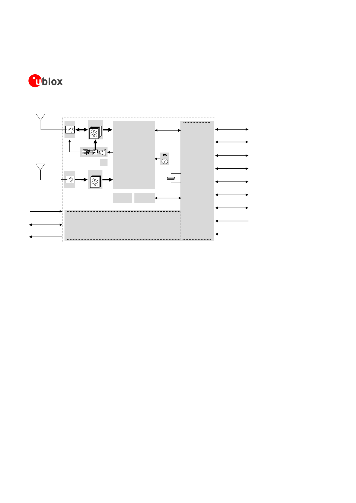
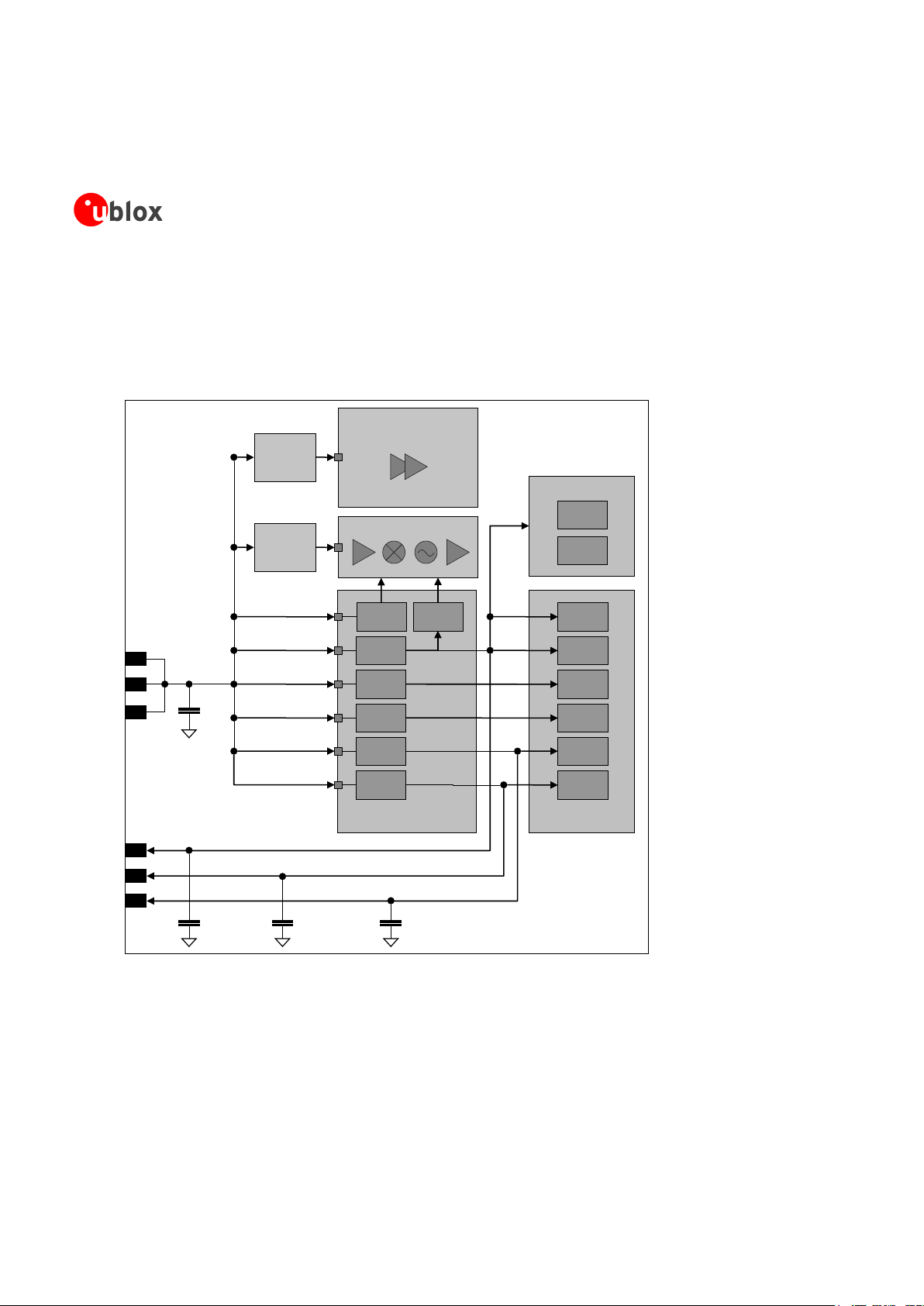
1.2 Architecture
Wireless
Base-band
Processor
Memory
Power Management Unit
26 MHz
32.768 kHz
ANT
Switch & Multi band & mode PA
DDC (for GNSS)
(U)SIM card
UART
SPI
USB
GPIO(s)
Power on
External reset
V_BCKP (RTC)
Vcc (supply)
V_INT (I/O)
Digital audio (I2S)
RF
SWITCH
RF
Transceiver
Duplexers
& Filters
ANT_DIV
RF
SWITCH
Filter
Bank
PA
PMU
Transceiver
PMU
Figure 1: LISA-U2 series block diagram (for available options see Table 2)
1.2.1 Functional blocks
LISA-U2 modules consist of the following internal functional blocks: RF section, Baseband and Power
Management Unit section.
LISA-U2 series RF section
A shielding box contains the RF high-power signal circuitry, including:
Multimode Single Chain Power Amplifier Module used for 3G HSPA/WCDMA and 2G EDGE/GSM operations
Power Management Unit with integrated DC/DC converter for the Power Amplifier Module
The RF antenna pad (ANT) is directly connected to the main antenna switch, which dispatches the RF signals
according to the active mode. For time-duplex 2G operation, the incoming signal at the active Receiver (RX) slot
is applied by the main antenna switch to the duplexer SAW filter bank for out-of-band rejection and then sent to
the appropriate receiver port of the RF transceiver. During the allocated Transmitter (TX) slots, the low level
signal coming from the RF transceiver is enhanced by the power amplifier and then directed to the antenna pad
through the main antenna switch. The 3G transmitter and receiver are active at the same time due to frequency domain duplex operation. The switch integrated in the main antenna switch connects the antenna port to the
duplexer SAW filter bank which separates the TX and RX signal paths. The duplexer itself provides front-end RF
filtering for RX band selection while combining the amplified TX signal coming from the power amplifier.
A separated shielding box contains all the other analog RF components, including:
Antenna Switch and duplexer SAW filter bank for main paths
Antenna Switch and SAW filter bank for diversity receiver
Up to six-band HSPA/WCDMA and quad-band EDGE/GPRS/GSM transceiver
Page 10

LISA-U2 series - System Integration Manual
UBX-13001118 - R19 Early Production Information System description
Page 10 of 175
Power Management Unit with integrated DC/DC converter for the Power Amplifier Module
Voltage Controlled Temperature Compensated 26 MHz Crystal Oscillator (VC-TCXO)
While operating in 3G mode, the RF transceiver performs direct up-conversion and down-conversion of the
baseband I/Q signals, with the RF voltage controlled gain amplifier being used to set the uplink TX power. In the
downlink path, the integrated LNA enhances the RX sensitivity while discrete inter-stage SAW filters additionally
improve the rejection of out-of-band blockers. An internal programmable gain amplifier optimizes the signal
levels before delivering to the analog I/Q to baseband for further digital processing.
For 2G operations, a constant gain direct conversion receiver with integrated LNAs and highly linear RF
quadrature demodulator are used to provide the same I/Q signals to the baseband as well. In transmission mode,
the up-conversion is implemented by means of a digital sigma-delta transmitter or polar modulator depending
on the modulation to be transmitted.
The RF antenna pad for the diversity receiver (ANT_DIV) available on LISA-U230 modules is directly connected to
the antenna switch for the diversity receiver, which dispatches the incoming RF signals to the dedicated SAW
filter bank for out-of-band rejection and then to the diversity receiver port of the RF transceiver.
In all the modes, a fractional-N sigma-delta RF synthesizer and an on-chip 3.296-4.340 GHz voltage controlled
oscillator are used to generate the local oscillator signal. The frequency reference to RF oscillators is provided by
the 26 MHz VC-TCXO. The same signal is buffered to the baseband as a master reference for clock generation
circuits while operating in active mode.
LISA-U2 series modulation techniques
Modulation techniques related to radio technologies supported by LISA-U2 modules, are listed as follows:
GSM GMSK
GPRS GMSK
EDGE GMSK / 8-PSK
WCDMA QPSK
HSDPA QPSK / 16-QAM
HSUPA QPSK / 16-QAM
LISA-U2 series Baseband and Power Management Unit section
Another shielding box of LISA-U2 modules includes all the digital circuitry and the power supplies, basically the
following functional blocks:
Cellular baseband processor, a mixed signal ASIC which integrates:
Microprocessor for controller functions, 2G & 3G upper layer software
DSP core for 2G Layer 1 and audio processing
3G coprocessor and HW accelerator for 3G Layer 1 control software and routines
Dedicated HW for interfaces management
Memory system in a Multi-Chip Package (MCP) integrating two devices:
NOR flash non-volatile memory
DDR SRAM volatile memory
Power Management Unit (PMU), used to derive all the system supply voltages from the module supply VCC
32.768 kHz crystal, connected to the Real Time Clock (RTC) oscillator to provide the clock reference in idle or
power-off mode
Page 11

LISA-U2 series - System Integration Manual
UBX-13001118 - R19 Early Production Information System description
Page 11 of 175
1.3 Pin-out
Table 3 lists the pin-out of the LISA-U2 modules, with pins grouped by function.
Function
Pin
Module
No
I/O
Description
Remarks
Power
VCC
All
61, 62, 63
I
Module supply
input
Clean and stable supply is required: low ripple and
low voltage drop must be guaranteed.
Voltage provided has to be always above the
minimum limit of the operating range.
Consider that there are large current spikes in
connected mode, when a GSM call is enabled.
VCC pins are internally connected, but all the
available pads must be connected to the external
supply in order to minimize power loss due to
series resistance.
See section 1.5.2
GND
All
1, 3, 6, 7,
8, 17, 25,
28, 29, 30,
31, 32, 33,
34, 35, 36,
37, 38, 60,
64, 65, 66,
67, 69, 70,
71, 72, 73,
75, 76
N/A
Ground
GND pins are internally connected but a good
(low impedance) external ground connection can
improve RF performance: all GND pins must be
externally connected to ground.
V_BCKP
All 2 I/O
Real Time Clock
supply
input/output
V_BCKP = 1.8 V (typical) generated by the module
when VCC supply voltage is within valid operating
range.
See section 1.5.4
V_INT
All 4 O
Digital Interfaces
supply output
V_INT = 1.8V (typical) generated by the module
when it is switched-on and the RESET_N (external
reset input pin) is not forced to the low level.
See section 1.5.5
VSIM
All
50 O SIM supply
output
VSIM = 1.80 V typical or 2.90 V typical generated
by the module according to the SIM card type.
See section 1.8
RF
ANT
All
68
I/O
RF input/output
for main Tx/Rx
antenna
50 nominal impedance.
See section 1.7, section 2.4 and section 2.2.1.1
ANT_DIV
LISA-U230
74 I RF input for Rx
diversity antenna
50 Ω nominal impedance
See section 1.7, section 2.4 and section 2.2.1.1
SIM
SIM_IO
All
48
I/O
SIM data
Internal 4.7 k pull-up to VSIM.
Must meet SIM specifications.
See section 1.8
SIM_CLK
All
47 O SIM clock
Must meet SIM specifications.
See section 1.8
SIM_RST
All
49 O SIM reset
Must meet SIM specifications.
See section 1.8
Page 12

LISA-U2 series - System Integration Manual
UBX-13001118 - R19 Early Production Information System description
Page 12 of 175
Function
Pin
Module
No
I/O
Description
Remarks
SPI
SPI_MISO
All
57 O SPI Data Line
Output
Module Output: module runs as an SPI slave.
Shift data on rising clock edge (CPHA=1).
Latch data on falling clock edge (CPHA=1).
Idle high.
See section 1.9.4
SPI_MOSI
All
56 I SPI Data Line
Input
Module Input: module runs as an SPI slave.
Shift data on rising clock edge (CPHA=1).
Latch data on falling clock edge (CPHA=1).
Idle high.
Internal active pull-up to V_INT (1.8 V) enabled.
See section 1.9.4
SPI_SCLK
All
55 I SPI Serial Clock
Input
Module Input: module runs as an SPI slave.
Idle low (CPOL=0).
Internal active pull-down to GND enabled.
See section 1.9.4
SPI_SRDY
All
58 O SPI Slave Ready
Output
Module Output: module runs as an SPI slave.
Idle low.
See section 1.9.4
SPI_MRDY
All
59 I SPI Master Ready
Input
Module Input: module runs as an SPI slave.
Idle low.
Internal active pull- down to GND enabled.
See section 1.9.4
DDC
SCL
All
45 O I2C bus clock line
Fixed open drain. External pull-up required.
See section 1.10
SDA
All
46
I/O
I2C bus data line
Fixed open drain. External pull-up required.
See section 1.10
UART
RxD
All
16 O UART data
output
Circuit 104 (RxD) in ITU-T V.24.
Provide access to the pin for FW update and
debugging if the USB interface is connected to the
application processor.
See section 1.9.2
TxD
All
15 I UART data input
Circuit 103 (TxD) in ITU-T V.24.
Internal active pull-up to V_INT (1.8 V) enabled.
Provide access to the pin for FW update and
debugging if the USB interface is connected to the
application processor.
See section 1.9.2
CTS
All
14 O UART clear to
send output
Circuit 106 (CTS) in ITU-T V.24.
Provide access to the pin for debugging if the USB
interface is connected to the application processor.
See section 1.9.2
RTS
All
13 I UART ready to
send input
Circuit 105 (RTS) in ITU-T V.24.
Internal active pull-up to V_INT (1.8 V) enabled.
Provide access to the pin for debugging if the USB
interface is connected to the application processor.
See section 1.9.2
DSR
All 9 O
UART data set
ready output
Circuit 107 (DSR) in ITU-T V.24.
See section 1.9.2
RI
All
10 O UART ring
indicator output
Circuit 125 (RI) in ITU-T V.24.
See section 1.9.2
DTR
All
12 I UART data
terminal ready
input
Circuit 108/2 (DTR) in ITU-T V.24.
Internal active pull-up to V_INT (1.8 V) enabled.
See section 1.9.2
DCD
All
11 O UART data carrier
detect output
Circuit 109 (DCD) in ITU-T V.24.
See section 1.9.2
Page 13

LISA-U2 series - System Integration Manual
UBX-13001118 - R19 Early Production Information System description
Page 13 of 175
Function
Pin
Module
No
I/O
Description
Remarks
GPIO
GPIO1
All
20
I/O
GPIO
See section 1.12
GPIO2
All
21
I/O
GPIO
See section 1.12
GPIO3
All
23
I/O
GPIO
See section 1.12
GPIO4
All
24
I/O
GPIO
See section 1.12
GPIO5
All
51
I/O
GPIO
See section 1.12
GPIO6
All
39
I/O
GPIO
See section 1.12
GPIO7
All
40
I/O
GPIO
See section 1.12
GPIO8
All
53
I/O
GPIO
See section 1.12
GPIO9
All
54
I/O
GPIO
See section 1.12
GPIO10
All
55
I/O
GPIO
See section 1.12
GPIO11
All
56
I/O
GPIO
See section 1.12
GPIO12
All
57
I/O
GPIO
See section 1.12
GPIO13
All
58
I/O
GPIO
See section 1.12
GPIO14
All
59
I/O
GPIO
See section 1.12
USB
VUSB_DET
All
18 I USB detect input
Input for VBUS (5 V typical) USB supply sense to
enable USB interface.
Provide access to the pin for FW update and
debugging if the USB interface is not connected to
the application processor.
See section 1.9.3
USB_D-
All
26
I/O
USB Data Line D-
90 Ω nominal differential impedance (Z0)
30 Ω nominal common mode impedance (ZCM)
Pull-up or pull-down resistors and external series
resistors as required by USB 2.0 specifications [7]
are part of the USB pad driver and need not be
provided externally.
Provide access to the pin for FW update and
debugging if the USB interface is not connected to
the application processor.
See section 1.9.3
USB_D+
All
27
I/O
USB Data Line
D+
90 Ω nominal differential impedance (Z0)
30 Ω nominal common mode impedance (ZCM)
Pull-up or pull-down resistors and external series
resistors as required by USB 2.0 specifications [7]
are part of the USB pad driver and need not be
provided externally.
Provide access to the pin for FW update and
debugging if the USB interface is not connected to
the application processor.
See section 1.9.3
System
PWR_ON
All
19 I Power-on input
PWR_ON pin has high input impedance.
Do not keep floating in noisy environment:
external pull-up required.
See section 1.6.1
RESET_N
All
22 I External reset
input
Internal 10 kΩ pull-up to V_BCKP.
See section 1.6.3
Page 14

LISA-U2 series - System Integration Manual
UBX-13001118 - R19 Early Production Information System description
Page 14 of 175
Function
Pin
Module
No
I/O
Description
Remarks
Digital
Audio
I2S_CLK
All
43
I/O
First I2S clock
Check device specifications to ensure compatibility
to module supported modes.
See section 1.11.
I2S_RXD
All
44 I First I2S receive
data
Internal active pull-down to GND enabled.
Check device specifications to ensure compatibility
to module supported modes.
See section 1.11.
I2S_TXD
All
42 O First I2S transmit
data
Check device specifications to ensure compatibility
to module supported modes.
See section 1.11.
I2S_WA
All
41
I/O
First I2S word
alignment
Check device specifications to ensure compatibility
to module supported modes.
See section 1.11.
I2S1_CLK
All
53
I/O
Second I2S clock
Check device specifications to ensure compatibility
to module supported modes.
See section 1.11.
I2S1_RXD
All
39 I Second I2S
receive data
Internal active pull-down to GND enabled.
Check device specifications to ensure compatibility
to module supported modes.
See section 1.11.
I2S1_TXD
All
40 O Second I2S
transmit data
Check device specifications to ensure compatibility
to module supported modes.
See section 1.11.
I2S1_WA
All
54
I/O
Second I2S word
alignment
Check device specifications to ensure compatibility
to module supported modes.
See section 1.11.
CODEC_CLK
All
52 O Clock output
Digital clock output for external audio codec
See section 1.11.
Reserved
RSVD
All 5 N/A
RESERVED pin
This pin must be connected to ground
See section 1.13
RSVD
LISA-U200
LISA-U201
LISA-U260
LISA-U270
74
N/A
RESERVED pin
Do not connect
See section 1.13
Table 3: LISA-U2 modules pin definition, grouped by function
Page 15

LISA-U2 series - System Integration Manual
UBX-13001118 - R19 Early Production Information System description
Page 15 of 175
1.4 Operating modes
LISA-U2 series modules have several operating modes. The operating modes are defined in Table 4 and
described in details in Table 5, providing general guidelines for operation.
General Status
Operating Mode
Definition
Power-down
Not-Powered Mode
VCC supply not present or below operating range: module is switched off.
Power-Off Mode
VCC supply within operating range and module is switched off.
Normal Operation
Idle-Mode
Module processor core runs with 32 kHz as reference oscillator.
Active-Mode
Module processor core runs with 26 MHz as reference oscillator.
Connected-Mode
Voice or data call enabled and processor core runs with 26 MHz as reference oscillator.
Table 4: Module operating modes definition
Operating
Mode
Description
Transition between operating modes
Not-Powered
Module is switched off.
Application interfaces are not accessible.
Internal RTC timer operates only if a valid
voltage is applied to V_BCKP pin.
When VCC supply is removed, the module enters not-powered mode.
When in not-powered mode, the module cannot be switched on by a
low pulse on PWR_ON input, by a rising edge on RESET_N input, or
by a preset RTC alarm.
When in not-powered mode, the module can be switched on applying
VCC supply (see 1.6.1) so that the module switches from not-powered
to active-mode.
Power-Off
Module is switched off: normal shutdown by an
appropriate power-off event (see 1.6.2).
Application interfaces are not accessible.
Only the internal RTC timer in operation.
When the module is switched off by an appropriate power-off event
(see 1.6.2), the module enters power-off mode from active-mode.
When in power-off mode, the module can be switched on by a low
pulse on PWR_ON input, by a rising edge on RESET_N input, or by a
preset RTC alarm (see 1.6.1): module switches from power-off to
active-mode.
When VCC supply is removed, the module switches from power-off
mode to not-powered mode.
Idle
Application interfaces are disabled: the module
does not accept data signals from an external
device connected to the module.
The module automatically enters idle-mode
whenever possible if power saving is enabled by
AT+UPSV (see u-blox AT Commands Manual
[2]), reducing current consumption (see 1.5.3.3).
If HW flow control is enabled (default setting)
and AT+UPSV=1 or AT+UPSV=3 has been set,
the UART CTS line indicates when the UART is
enabled (see 1.9.2.2, 1.9.2.3).
If HW flow control is disabled by AT&K0, the
UART CTS line is fixed to ON state (see 1.9.2.2).
Power saving configuration is not enabled by
default: it can be enabled by AT+UPSV (see the
u-blox AT Commands Manual [2]).
The module automatically switches from active-mode to idle-mode
whenever possible if power saving is enabled (see 1.5.3.3, 1.9.2.3,
1.9.3.2, 1.9.4.2 and u-blox AT Commands Manual [2], AT+UPSV).
The module wakes up from idle-mode to active-mode in these events:
Automatic periodic monitoring of the paging channel for the
paging block reception according to network conditions (see
1.5.3.3, 1.9.2.3)
Automatic periodic enable of the UART interface to receive and
send data, if AT+UPSV=1 has been set (see 1.9.2.3)
RTC alarm occurs (see u-blox AT Commands Manual [2],
AT+CALA)
Data received on UART interface, if HW flow control has been
disabled by AT&K0 and AT+UPSV=1 has been set (see 1.9.2.3)
RTS input set ON by the DTE if HW flow control has been
disabled by AT&K0 and AT+UPSV=2 has been set (see 1.9.2.3)
DTR input set ON by DTE if AT+UPSV=3 has been set (see 1.9.2.3)
USB detection, applying 5 V (typ.) to VUSB_DET input (see 1.9.3)
The connected USB host forces a remote wakeup of the module
as USB device (see 1.9.3)
The connected SPI master indicates by the SPI_MRDY input signal
that it is ready for transmission or reception (see 1.9.4)
The connected u-blox GNSS receiver indicates by the GPIO3 pin
that it is ready to send data (see 1.10, 1.12)
Page 16

LISA-U2 series - System Integration Manual
UBX-13001118 - R19 Early Production Information System description
Page 16 of 175
Operating
Mode
Description
Transition between operating modes
Active
The module is ready to accept data signals from
an external device unless power saving
configuration is enabled by AT+UPSV (see
sections 1.9.2.3, 1.9.3.2, 1.9.4.2 and u-blox AT
Commands Manual [2]).
When the module is switched on by an appropriate power-on event
(see 1.6.1), the module enters active-mode from not-powered or
power-off mode.
If power saving configuration is enabled by the AT+UPSV command,
the module automatically switches from active to idle-mode whenever
possible and the module wakes up from idle to active-mode in the
events listed above (see the idle to active transition description).
When a voice call or a data call is initiated, the module switches from
active-mode to connected-mode.
Connected
A voice call or a data call is in progress.
When a voice or a data call is enabled, the
application interfaces are kept enabled and the
module is prepared to accept data from an
external device unless power saving
configuration is enabled by AT+UPSV (see
1.9.2.3, 1.9.3.2, 1.9.4.2 and u-blox AT
Commands Manual [2]).
When a voice call or a data call is initiated, the module enters
connected-mode from active-mode.
If power saving configuration is enabled by the AT+UPSV command,
the module automatically switches from connected to idle-mode
whenever possible in case of PSD data call with internal context
activation, and then it wakes up from idle to connected mode in the
events listed above (see the idle to active transition description).
When a voice call or a data call is terminated, the module returns to
the active-mode.
Table 5: Module operating modes description
Figure 2 describes the transition between the different operating modes.
Switch ON:
• Apply VCC
If power saving is enabled
and there is no activity for
a defined time interval
Any wake up event described
in the module operating
modes summary table above
Incoming/outgoing call or
other dedicated device
network communication
Call terminated,
communication dropped
Remove VCC
Switch ON:
• PWR_ON
• RESET_N
• RTC Alarm
Not
powered
Power off
ActiveConnected Idle
Switch OFF:
• AT+CPWROFF
• PWR_ON
Figure 2: Operating modes transition
Page 17
LISA-U2 series - System Integration Manual
UBX-13001118 - R19 Early Production Information System description
Page 17 of 175
1.5 Power management
1.5.1 Power supply circuit overview
LISA-U2 series modules feature a power management concept optimized for the most efficient use of supplied
power. This is achieved by hardware design utilizing a power efficient circuit topology (Figure 3), and by power
management software controlling the module’s power saving mode.
Baseband Processor
2G/3G
Power Amplifier(s)
Switching
Step-Down
5 x 10 µF
61
VCC
62
VCC
63
VCC
50
VSIM
2
V_BCKP
4
V_INT
Linear
LDO
Linear
LDO
Switching
Step-Down
Linear
LDO
Linear
LDO
Linear
LDO
I/O
EBU
CORE
Analog
SIM
RTC
NOR Flash
DDR SRAM
RF Transceiver
Memory
Power Management Unit
22 µF
220 nF
220 nF
2G/3G PA
PMU
Transceiver
PMU
Figure 3: LISA-U2 series power management simplified block diagram
Page 18

LISA-U2 series - System Integration Manual
UBX-13001118 - R19 Early Production Information System description
Page 18 of 175
Pins with supply function are reported in Table 6, Table 12 and Table 15.
LISA-U2 series modules must be supplied via the VCC pins. There is only one main power supply input, available
on the three VCC pins that must be all connected to the external power supply.
The VCC pins are directly connected to the RF power amplifiers and to the integrated Power Management Unit
(PMU) within the module: all supply voltages needed by the module are generated from the VCC supply by
integrated voltage regulators.
V_BCKP is the Real Time Clock (RTC) supply. When the VCC voltage is within the valid operating range, the
internal PMU supplies the Real Time Clock and the same supply voltage will be available to the V_BCKP pin. If
the VCC voltage is under the minimum operating limit (for example, during not powered mode), the Real Time
Clock can be externally supplied via the V_BCKP pin (see section 1.5.4).
When a 1.8 V or a 3 V SIM card type is connected, LISA-U2 series modules automatically supply the SIM card via
the VSIM pin. Activation and deactivation of the SIM interface with automatic voltage switch from 1.8 to 3 V is
implemented, in accordance to the ISO-IEC 7816-3 specifications.
The same voltage domain used internally to supply the digital interfaces is also available on the V_INT pin, to
allow more economical and efficient integration of the LISA-U2 series modules in the final application.
The integrated Power Management Unit also provides the control state machine for system start up and system
reset control.
1.5.2 Module supply (VCC)
The LISA-U2 series modules must be supplied through the VCC pins by a DC power supply. Voltages must be
stable: during operation, the current drawn from VCC can vary by some orders of magnitude, especially due to
surging consumption profile of the GSM system (described in the section 1.5.3). It is important that the system
power supply circuit is able to support peak power (see LISA-U2 series Data Sheet [1] for the detailed
specifications).
Name
Description
Remarks
VCC
Module power supply input
VCC pins are internally connected, but all the available pads
must be connected to the external supply in order to
minimize the power loss due to series resistance.
Clean and stable supply is required: low ripple and low
voltage drop must be guaranteed.
Voltage provided must always be above the minimum limit of
the operating range.
Consider that during a GSM call there are large current spikes
in connected mode.
GND
Ground
GND pins are internally connected but a good (low
impedance) external ground can improve RF performance: all
available pads must be connected to ground.
Table 6: Module supply pins
VCC pins ESD sensitivity rating is 1 kV (Human Body Model according to JESD22-A114F). Higher
protection level can be required if the line is externally accessible on the application board. Higher
protection level can be achieved by mounting an ESD protection (e.g. EPCOS CA05P4S14THSG varistor
array) on the line connected to this pin, close to accessible point.
The voltage provided to the VCC pins must be within the normal operating range limits as specified in the
LISA-U2 series Data Sheet [1]. Complete functionality of the module is only guaranteed within the specified
minimum and maximum VCC voltage normal operating range.
Page 19
LISA-U2 series - System Integration Manual
UBX-13001118 - R19 Early Production Information System description
Page 19 of 175
The module cannot be switched on if the VCC voltage value is below the specified normal operating
range minimum limit. Ensure that the input voltage at VCC pins is above the minimum limit of the normal
operating range for more than 3 s after the start of the module switch-on sequence.
When LISA-U2 series modules are in operation, the voltage provided to VCC pins can go outside the normal
operating range limits but must be within the extended operating range limits specified in LISA-U2 series Data
Sheet [1]. Occasional deviations from the ETSI specifications may occur when the input voltage at VCC pins is
outside the normal operating range and is within the extended operating range.
LISA-U2 series modules switch off when VCC voltage value drops below the specified extended operating
range minimum limit: ensure that the input voltage at VCC pins never drops below the minimum limit of
the extended operating range when the module is switched on, not even during a GSM transmit burst,
where the current consumption can rise up to maximum peaks of 2.5 A in case of a mismatched antenna
load.
Operation above the normal operating range maximum limit is not recommended and extended
exposure beyond it may affect device reliability.
Stress beyond the VCC absolute maximum ratings can cause permanent damage to the module:
if necessary, voltage spikes beyond VCC absolute maximum ratings must be restricted to values
within the specified limits by using appropriate protection.
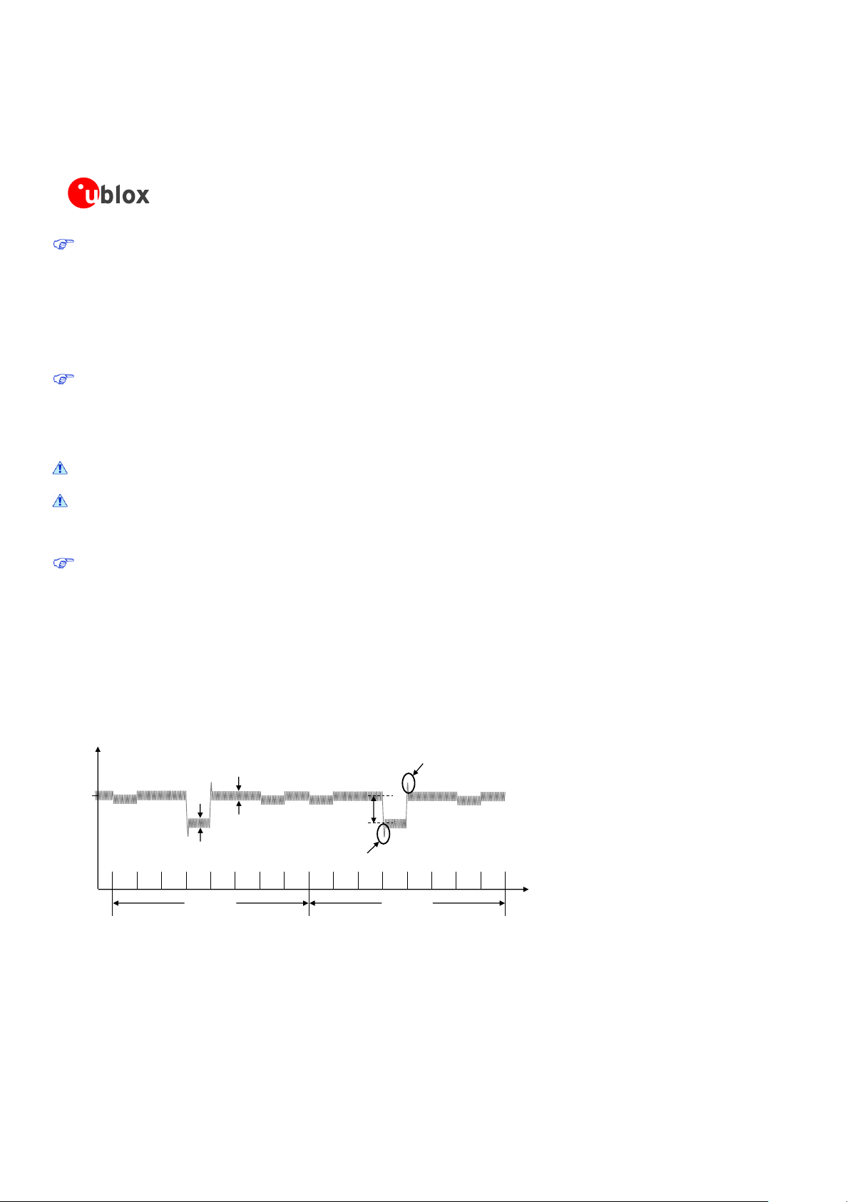
When designing the power supply for the application, pay specific attention to power losses and
transients. The DC power supply must be able to provide a voltage profile to the VCC pins with the
following characteristics:
o Voltage drop during transmit slots must be lower than 400 mV
o No undershoot or overshoot at the start and at the end of transmit slots
o Voltage ripple during transmit slots must be minimized:
lower than 70 mVpp if f
ripple
≤ 200 kHz
lower than 10 mVpp if 200 kHz < f
ripple
≤ 400 kHz
lower than 2 mVpp if f
ripple
> 400 kHz
Time
undershoot
overshoot
ripple
ripple
drop
Voltage
3.8 V
(typ)
RX
slot
unused
slot
unused
slot
TX
slot
unused
slot
unused
slot
MON
slot
unused
slot
RX
slot
unused
slot
unused
slot
TX
slot
unused
slot
unused
slot
MON
slot
unused
slot
GSM frame
4.615 ms
(1 frame = 8 slots)
GSM frame
4.615 ms
(1 frame = 8 slots)
Figure 4: Description of the VCC voltage profile versus time during a GSM call
Page 20
LISA-U2 series - System Integration Manual
UBX-13001118 - R19 Early Production Information System description
Page 20 of 175
Any degradation in power supply performance (due to losses, noise or transients) will directly affect the RF
performance of the module since the single external DC power source indirectly supplies all the digital and
analog interfaces, and also directly supplies the RF power amplifier (PA).
The voltage at the VCC pins must ramp from 2.5 V to 3.2 V within 1 ms. This VCC slope allows a proper
switch on of the module when the voltage rises to the VCC normal operating range from a voltage of less
than 2.25 V. If the external supply circuit cannot raise the VCC voltage from 2.5 V to 3.2 V within 1 ms,
the RESET_N pin should be kept low during VCC rising edge, so that the module will switch on releasing
the RESET_N pin when the VCC voltage stabilizes at its nominal value within the normal operating range.
1.5.2.1 VCC application circuits
LISA-U2 series modules must be supplied through the VCC pins by a proper DC power supply, which can be
selected according to the application requirements (see Figure 5) between the different possible supply sources
types, which most common ones are the following:
Switching regulator
Low Drop-Out (LDO) linear regulator
Rechargeable Lithium-ion (Li-Ion) or Lithium-ion polymer (Li-Pol) battery
Primary (disposable) battery
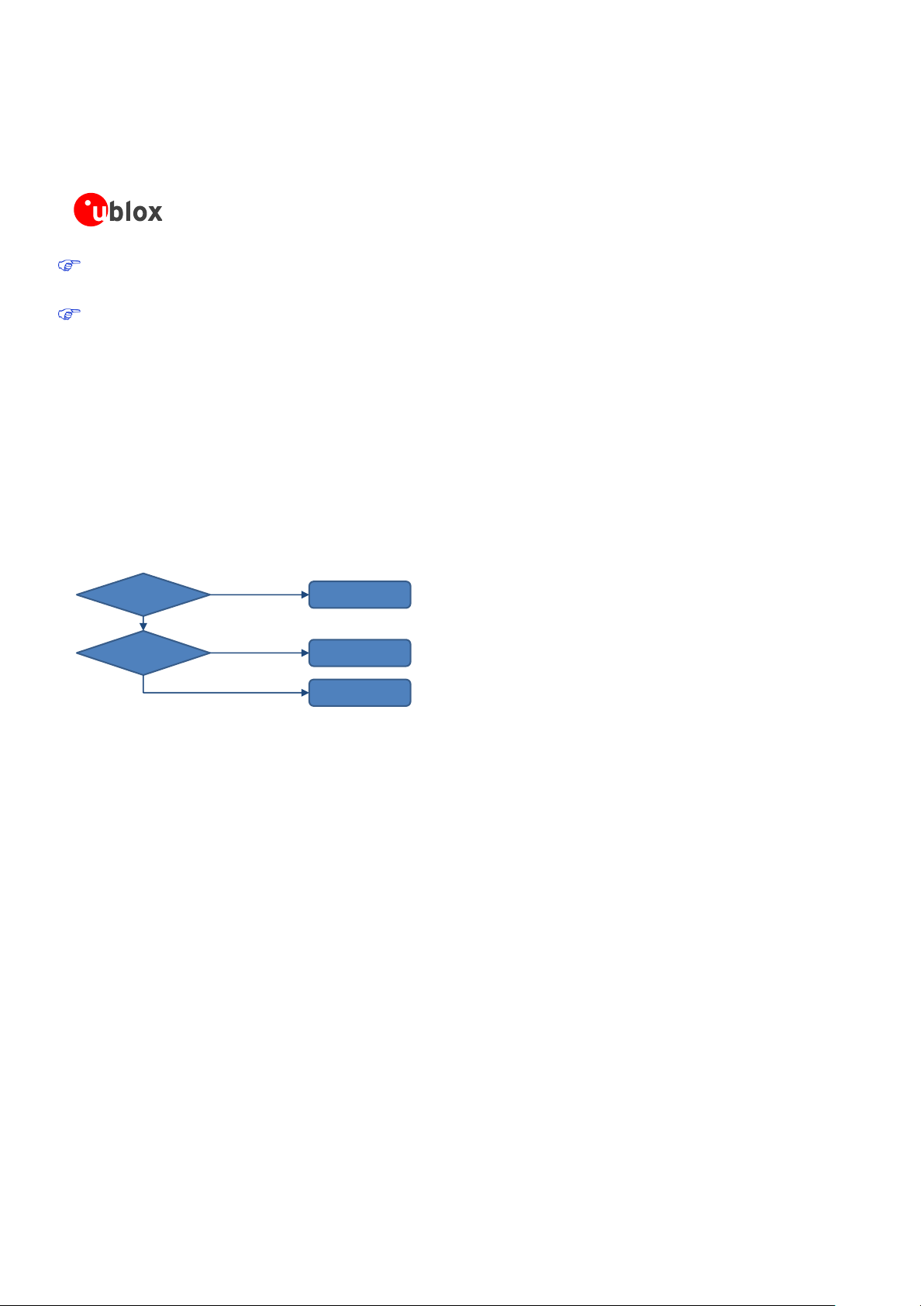
Main Supply
Available?
Battery
Li-Ion 3.7 V
Linear LDO
Regulator
Main Supply
Voltage > 5V?
Switching Step-Down
Regulator
No, portable device
No, less than 5 V
Yes, greater than 5 V
Yes, always available
Figure 5: VCC supply concept selection
The switching step-down regulator is the typical choice when the available primary supply source has a nominal
voltage much higher (e.g. greater than 5 V) than the LISA-U2 series modules operating supply voltage. The use
of switching step-down provides the best power efficiency for the overall application and minimizes current
drawn from the main supply source.
The use of an LDO linear regulator becomes convenient for a primary supply with a relatively low voltage (e.g.
less than 5 V). In this case the typical 90% efficiency of the switching regulator will diminish the benefit of
voltage step-down and no true advantage will be gained in input current savings. On the opposite side, linear
regulators are not recommended for high voltage step-down as they will dissipate a considerable amount of
energy in thermal power.
If LISA-U2 series modules are deployed in a mobile unit where no permanent primary supply source is av ailable,
then a battery will be required to provide VCC. A standard 3-cell Li-Ion or Li-Pol battery pack directly connected
to VCC is the usual choice for battery-powered devices. During charging, batteries with Ni-MH chemistry
typically reach a maximum voltage that is above the maximum rating for VCC, and should therefore be avoided.
The use of primary (not rechargeable) battery is uncommon, since the most cells available are seldom capable of
delivering the burst peak current for a GSM call due to high internal resistance.
Keep in mind that the use of batteries requires the implementation of a suitable charger circuit (not included in
LISA-U2 series modules). The charger circuit should be designed in order to prevent over-voltage on VCC beyond
the upper limit of the absolute maximum rating.
The usage of more than one DC supply at the same time should be carefully evaluated: depending on the supply
source characteristics, different DC supply systems can result as mutually exclusive.
Page 21

LISA-U2 series - System Integration Manual
UBX-13001118 - R19 Early Production Information System description
Page 21 of 175
The usage of a regulator or a battery not able to withstand the maximum VCC peak current consumption stated
in LISA-U2 series Data Sheet [1] is generally not recommended. However, if the selected regulator or battery is
not able to withstand the maximum VCC peak current, it must be able to withstand at least the maximum
average current consumption value specified in the module data sheet Error! Reference source not found..
The additional energy required by the module during a GSM/GPRS Tx slot (when in the worst case the current
consumption can rise up to 2.5 A, as described in section 1.5.3.1) can be provided by an appropriate bypass tank
capacitor or supercapacitor with very large capacitance and very low ESR placed close to the module VCC pins.
Depending on the actual capability of the selected regulator or battery, the required capacitance can be
considerably larger than 1 mF and the required ESR can be in the range of few tens of m. Carefully evaluate
the implementation of this solution since aging and temperature conditions significantly affect the actual
capacitor characteristics.
The following sections highlight some design aspects for each of the supplies listed above.
Switching regulator
The characteristics of the switching regulator connected to VCC pins should meet the following requirements:
Power capability: the switching regulator with its output circuit must be capable of providing a voltage
value to the VCC pins within the specified operating range and must be capable of delivering 2.5 A current
pulses with 1/8 duty cycle to the VCC pins
Low output ripple: the switching regulator together with its output circuit must be capable of providing a
clean (low noise) VCC voltage profile
High switching frequency: for best performance and for smaller applications select a switching frequency
≥ 600 kHz (since L-C output filter is typically smaller for high switching frequency). The use of a switching
regulator with a variable switching frequency or with a switching frequency lower than 600 kHz must be
carefully evaluated since this can produce noise in the VCC voltage profile and therefore negatively impact
GSM modulation spectrum performance. An additional L-C low-pass filter between the switching regulator
output to VCC supply pins can mitigate the ripple on VCC, but adds extra voltage drop due to resistive
losses on series inductors
PWM mode operation: select preferably regulators with Pulse Width Modulation (PWM) mode. While in
connected mode Pulse Frequency Modulation (PFM) mode and PFM/PWM mode transitions must be avoided
to reduce the noise on the VCC voltage profile. Switching regulators able to switch between low ripple
PWM mode and high efficiency burst or PFM mode can be used, provided the mode transition occurs when
the module changes status from idle/active mode to connected mode (where current consumption increases
to a value greater than 100 mA): it is permissible to use a regulator that switches from the PWM mode to
the burst or PFM mode at an appropriate current threshold (e.g. 60 mA)
Output voltage slope: the use of the soft start function provided by some voltage regulator must be
carefully evaluated, since the voltage at the VCC pins must ramp from 2.5 V to 3.2 V within 1 ms to allow a
proper switch-on of the module
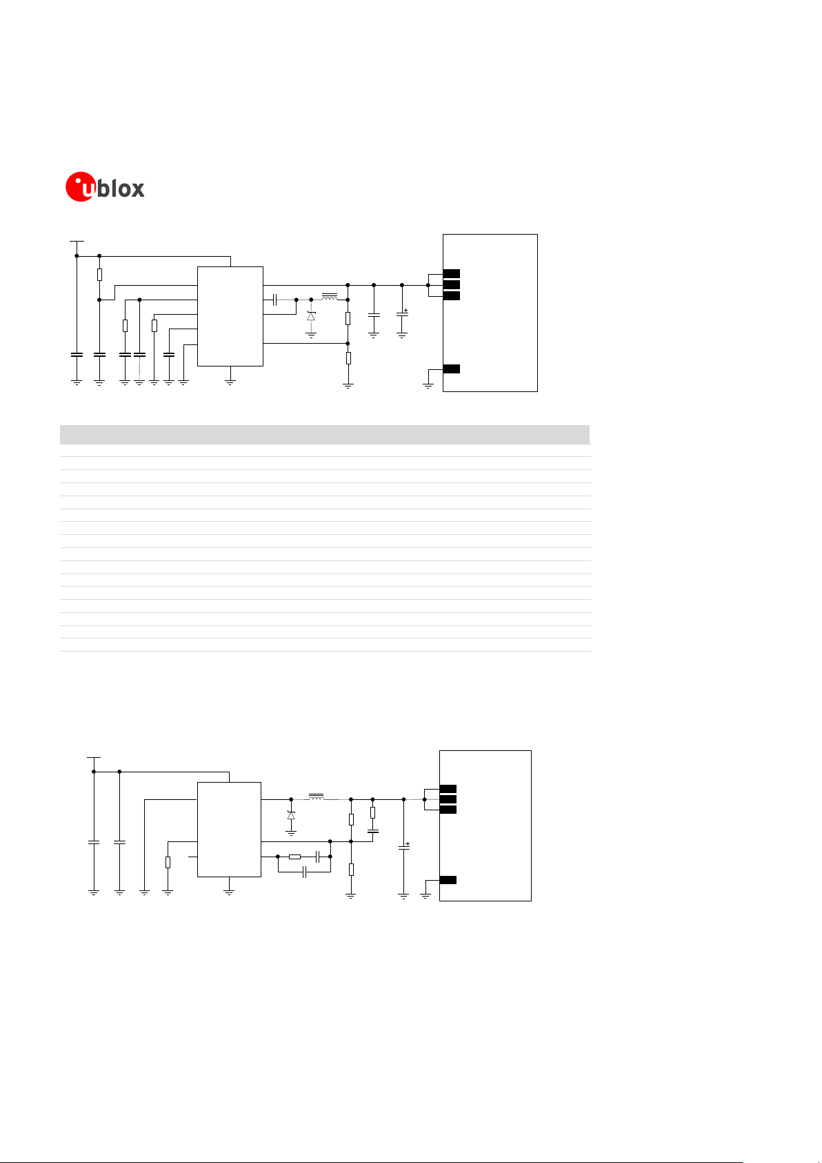
Figure 6 and the components listed in Table 7 show an example of a high reliability power supply circuit, where
the module VCC is supplied by a step-down switching regulator capable of delivering 2.5 A current pulses with
low output ripple and with fixed switching frequency in PWM mode operation greater than 1 MHz. The use of a
switching regulator is suggested when the difference from the available supply rail to the VCC value is high:
switching regulators provide good efficiency transforming a 12 V supply to the typical 3.8 V value of the VCC
supply.
Page 22
LISA-U2 series - System Integration Manual
UBX-13001118 - R19 Early Production Information System description
Page 22 of 175
LISA-U2 series
12V
C5
R3
C4
R2
C2C1
R1
VIN
RUN
VC
RT
PG
SYNC
BD
BOOST
SW
FB
GND
6
7
10
9
5
C612
3
8
11
4
C7 C8
D1
R4
R5
L1
C3
U1
62
VCC
63
VCC
61
VCC
GND
Figure 6: Suggested schematic design for the VCC voltage supply application circuit using a step-down regulator
Reference
Description
Part Number - Manufacturer
C1
10 µF Capacitor Ceramic X7R 5750 15% 50 V
C5750X7R1H106MB - TDK
C2
10 nF Capacitor Ceramic X7R 0402 10% 16 V
GRM155R71C103KA01 - Murata
C3
680 pF Capacitor Ceramic X7R 0402 10% 16 V
GRM155R71H681KA01 - Murata
C4
22 pF Capacitor Ceramic COG 0402 5% 25 V
GRM1555C1H220JZ01 - Murata
C5
10 nF Capacitor Ceramic X7R 0402 10% 16 V
GRM155R71C103KA01 - Murata
C6
470 nF Capacitor Ceramic X7R 0603 10% 25 V
GRM188R71E474KA12 - Murata
C7
22 µF Capacitor Ceramic X5R 1210 10% 25 V
GRM32ER61E226KE15 - Murata
C8
330 µF Capacitor Tantalum D_SIZE 6.3 V 45 mΩ
T520D337M006ATE045 - KEMET
D1
Schottky Diode 40 V 3 A
MBRA340T3G - ON Semiconductor
L1
10 µH Inductor 744066100 30% 3.6 A
744066100 - Wurth Electronics
R1
470 kΩ Resistor 0402 5% 0.1 W
2322-705-87474-L - Yageo
R2
15 kΩ Resistor 0402 5% 0.1 W
2322-705-87153-L - Yageo
R3
22 kΩ Resistor 0402 5% 0.1 W
2322-705-87223-L - Yageo
R4
390 kΩ Resistor 0402 1% 0.063 W
RC0402FR-07390KL - Yageo
R5
100 kΩ Resistor 0402 5% 0.1 W
2322-705-70104-L - Yageo
U1
Step Down Regulator MSOP10 3.5 A 2.4 MHz
LT3972IMSE#PBF - Linear Technology
Table 7: Suggested components for the VCC voltage supply application circuit using a step-down regulator
Figure 7 and the components listed in Table 8 show an example of a low cost power supply circuit, where the
VCC module supply is provided by a step-down switching regulator capable of delivering 2.5 A current pulses,
transforming a 12 V supply input.
LISA-U2 series
12V
R5
C6C1
VCC
INH
FSW
SYNC
OUT
GND
2
6
3
1
7
8
C3
C2
D1
R1
R2
L1
U1
GND
FB
COMP
5
4
R3
C4
R4
C5
62
VCC
63
VCC
61
VCC
Figure 7: Suggested low cost solution for the VCC voltage supply application circuit using step-down regulator
Page 23

LISA-U2 series - System Integration Manual
UBX-13001118 - R19 Early Production Information System description
Page 23 of 175
Reference
Description
Part Number - Manufacturer
C1
22 µF Capacitor Ceramic X5R 1210 10% 25 V
GRM32ER61E226KE15 – Murata
C2
100 µF Capacitor Tantalum B_SIZE 20% 6.3V 15m
T520B107M006ATE015 – Kemet
C3
5.6 nF Capacitor Ceramic X7R 0402 10% 50 V
GRM155R71H562KA88 – Murata
C4
6.8 nF Capacitor Ceramic X7R 0402 10% 50 V
GRM155R71H682KA88 – Murata
C5
56 pF Capacitor Ceramic C0G 0402 5% 50 V
GRM1555C1H560JA01 – Murata
C6
220 nF Capacitor Ceramic X7R 0603 10% 25 V
GRM188R71E224KA88 – Murata
D1
Schottky Diode 25V 2 A
STPS2L25 – STMicroelectronics
L1
5.2 µH Inductor 30% 5.28A 22 m
MSS1038-522NL – Coilcraft
R1
4.7 k Resistor 0402 1% 0.063 W
RC0402FR-074K7L – Yageo
R2
910 Resistor 0402 1% 0.063 W
RC0402FR-07910RL – Yageo
R3
82 Resistor 0402 5% 0.063 W
RC0402JR-0782RL – Yageo
R4
8.2 k Resistor 0402 5% 0.063 W
RC0402JR-078K2L – Yageo
R5
39 k Resistor 0402 5% 0.063 W
RC0402JR-0739KL – Yageo
U1
Step-Down Regulator 8-VFQFPN 3 A 1 MHz
L5987TR – ST Microelectronics
Table 8: Suggested components for low cost solution VCC voltage supply application circuit using a step-down regulator
Low Drop-Out (LDO) linear regulator
The characteristics of the LDO linear regulator connected to the VCC pins should meet the following
requirements:
Power capabilities: the LDO linear regulator with its output circuit must be capable of providing a proper
voltage value to the VCC pins and of delivering 2.5 A current pulses with 1/8 duty cycle
Power dissipation: the power handling capability of the LDO linear regulator must be checked to limit its
junction temperature to the maximum rated operating range (i.e. check the voltage drop from the max input
voltage to the min output voltage to evaluate the power dissipation of the regulator)
Output voltage slope: the use of the soft start function provided by some voltage regulators must be
carefully evaluated, since the voltage at the VCC pins must ramp from 2.5 V to 3.2 V within 1 ms to allow a
proper switch-on of the module
Figure 8 and the components listed in Table 9 show an example of a power supply circuit, where the VCC
module supply is provided by an LDO linear regulator capable of delivering 2.5 A current pulses, with proper
power handling capability. The use of a linear regulator is suggested when the difference from the available
supply rail and the VCC value is low: linear regulators provide high efficiency when transforming a 5 V supply to
a voltage value within the module VCC normal operating range.
It is recommended to configure the LDO linear regulator so that it generates a voltage supply value slightly
below the maximum limit of the module VCC normal operating range (e.g. ~4.1 V as in the circuit described in
Figure 8 and Table 9). This reduces the power on the linear regulator and improves the thermal design of the
supply circuit.
Page 24
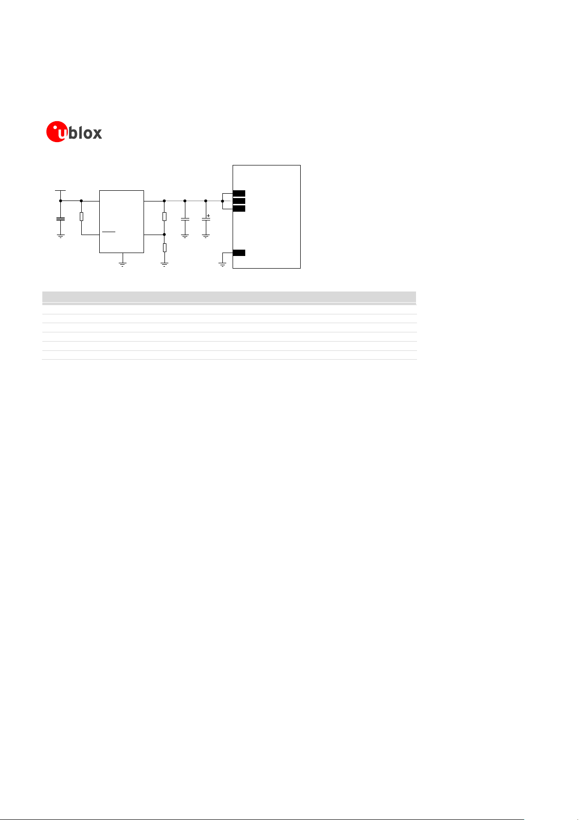
LISA-U2 series - System Integration Manual
UBX-13001118 - R19 Early Production Information System description
Page 24 of 175
5V
C1 R1
IN OUT
ADJ
GND
1
2
4
5
3
C2R2
R3
U1
SHDN
LISA-U2 series
62
VCC
63
VCC
61
VCC
GND
C3
Figure 8: Suggested schematic design for the VCC voltage supply application circuit using an LDO linear regulator
Reference
Description
Part Number - Manufacturer
C1, C2
10 µF Capacitor Ceramic X5R 0603 20% 6.3 V
GRM188R60J106ME47 - Murata
C3
330 µF Capacitor Tantalum D_SIZE 6.3 V 45 mΩ
T520D337M006ATE045 - KEMET
R1
47 kΩ Resistor 0402 5% 0.1 W
RC0402JR-0747KL - Yageo Phycomp
R2
9.1 kΩ Resistor 0402 5% 0.1 W
RC0402JR-079K1L - Yageo Phycomp
R3
3.9 kΩ Resistor 0402 5% 0.1 W
RC0402JR-073K9L - Yageo Phycomp
U1
LDO Linear Regulator ADJ 3.0 A
LT1764AEQ#PBF - Linear Technology
Table 9: Suggested components for VCC voltage supply application circuit using an LDO linear regulator
Rechargeable Li-Ion or Li-Pol battery
Rechargeable Li-Ion or Li-Pol batteries connected to the VCC pins should meet the following requirements:
Maximum pulse and DC discharge current: the rechargeable Li-Ion battery with its output circuit must be
capable of delivering 2.5 A current pulses with 1/8 duty-cycle to the VCC pins and must be capable of
delivering a DC current greater than the module maximum average current consumption to VCC pins. The
maximum pulse discharge current and the maximum DC discharge current are not always reported in
battery data sheets, but the maximum DC discharge current is typically almost equal to the battery capacity
in Amp-hours divided by 1 hour
DC series resistance: the rechargeable Li-Ion battery with its output circuit must be capable of avoiding a
VCC voltage drop greater than 400 mV during transmit bursts
Primary (disposable) battery
The characteristics of a primary (non-rechargeable) battery connected to VCC pins should meet the following
requirements:
Maximum pulse and DC discharge current: the non-rechargeable battery with its output circuit must be
capable of delivering 2.5 A current pulses with 1/8 duty-cycle to the VCC pins and must be capable of
delivering a DC current greater than the module maximum average current consumption at the VCC pins.
The maximum pulse and the maximum DC discharge current is not always reported in battery data sheets,
but the maximum DC discharge current is typically almost equal to the battery capacity in Amp-hours
divided by 1 hour
DC series resistance: the non-rechargeable battery with its output circuit must be capable of avoiding a
VCC voltage drop greater than 400 mV during transmit bursts
Page 25
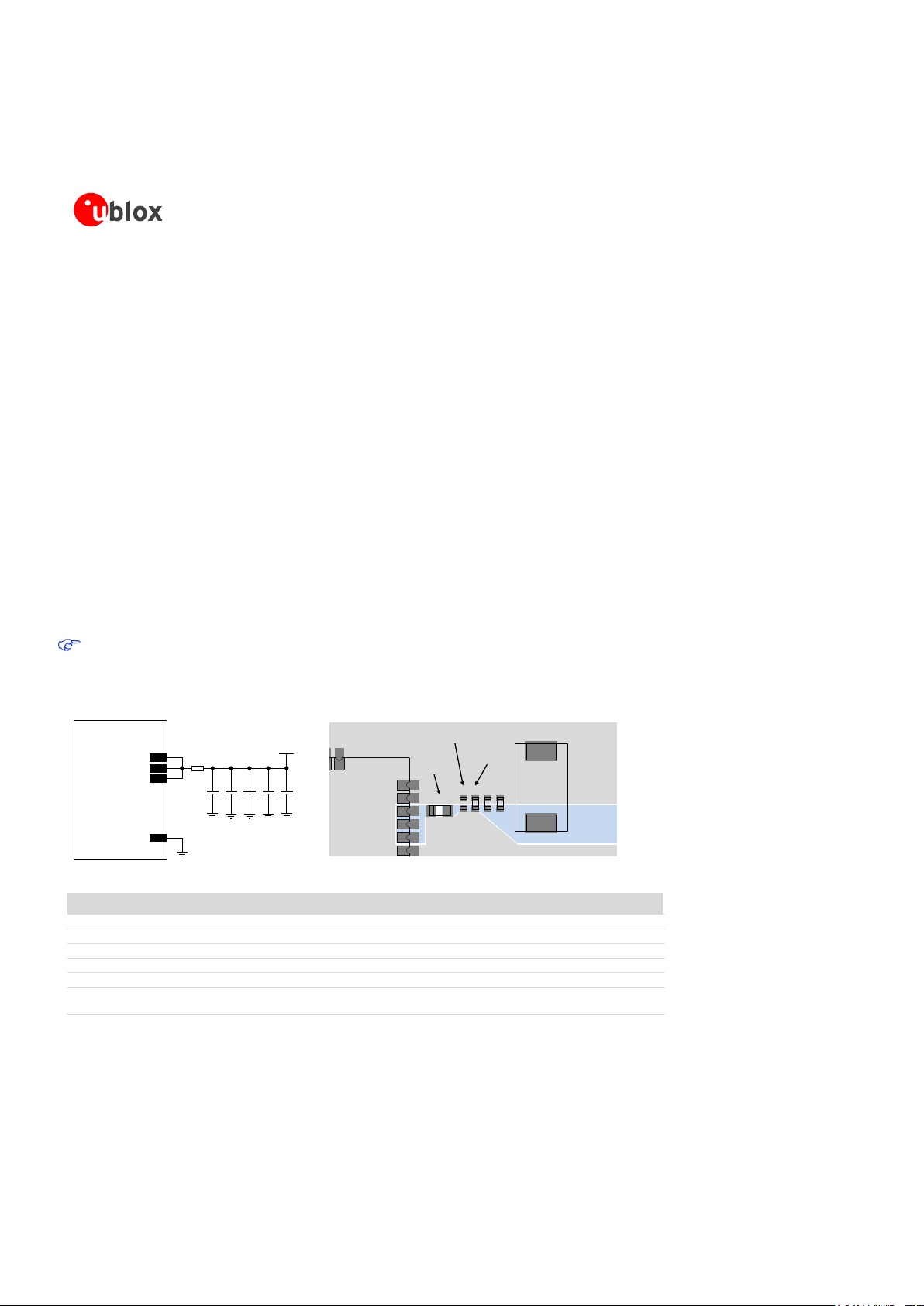
LISA-U2 series - System Integration Manual
UBX-13001118 - R19 Early Production Information System description
Page 25 of 175
Additional recommendations for the VCC supply application circuits
To reduce voltage drops, use a low impedance power source. The resistance of the power supply lines
(connected to the VCC and GND pins of the module) on the application board and battery pack should also be
considered and minimized: cabling and routing must be as short as possible in order to minimize power losses.
It is recommended to properly connect all three VCC pins and all twenty GND pins of the module to the supply
source to minimize series resistance losses.
To avoid voltage drop undershoot and overshoot at the start and end of a transmit burst during a GSM call
(when current consumption on the VCC supply can rise up to as much as 2.5 A in the worst case), place a bypass
capacitor with large capacitance (more than 100 µF) and low ESR near the VCC pins, for example:
330 µF capacitance, 45 mΩ ESR (e.g. KEMET T520D337M006ATE045, Tantalum Capacitor)
The use of very large capacitors (i.e. greater then 1000 µF) on the VCC line and the use of the soft start function
provided by some voltage regulators must be carefully evaluated, since the voltage at the VCC pins must ramp
from 2.5 V to 3.2 V within 1 ms to allow a proper switch on of the module.
To reduce voltage ripple and noise, which should improve RF performance if the application device integrates an
internal antenna, place the following series ferrite bead and bypass capacitors near the VCC pins of the module:
Ferrite bead for GHz band noise (e.g. Murata BLM18EG221SN1) as close as possible to the VCC pins of the
module, implementing the circuit described in Figure 9, to filter EMI in all the GSM / UMTS bands.
68 pF capacitor with Self-Resonant Frequency in the 800/900 MHz range (e.g. Murata GRM1555C1H680J)
at the VCC line where it narrows close to the module (see Figure 9), to filter EMI in lower bands
15 pF capacitor with Self-Resonant Frequency in 1800/1900 MHz range (e.g. Murata GRM1555C1H150J)
at the VCC line where it narrows close to the module (see Figure 9), to filter EMI in higher bands
10 nF capacitor (e.g. Murata GRM155R71C103K) to filter digital logic noise from clocks and data sources
100 nF capacitor (e.g. Murata GRM155R61A104K) to filter digital logic noise from clocks and data sources
Figure 9 shows the complete configuration, but keep in mind that the mounting of each single
component depends on the application design. It is highly recommended to provide the series ferrite bead
and all the VCC bypass capacitors as described in Figure 9 and Table 10 if the application device integrates
an internal antenna.
C1
GND
C2 C4
LISA-U2 series
62
VCC
63
VCC
61
VCC
3V8
C5
+
LISA-U
series
C5
GND plane
VCC line
Capacitor with
SRF ~900 MHz
FB1
C1 C3 C4
FB1
Ferrite Bead
for GHz noise
C2
C3
Capacitor with
SRF ~1900 MHz
Figure 9: Suggested schematic and layout design for the VCC line; highly recommended when using an integrated antenna
Reference
Description
Part Number - Manufacturer
C1
68 pF Capacitor Ceramic C0G 0402 5% 50 V
GRM1555C1H680JA01 - Murata
C2
15 pF Capacitor Ceramic C0G 0402 5% 50 V
GRM1555C1H150JA01 - Murata
C3
10 nF Capacitor Ceramic X7R 0402 10% 16 V
GRM155R71C103KA01 - Murata
C4
100 nF Capacitor Ceramic X7R 0402 10% 16 V
GRM155R71C104KA01 - Murata
C5
330 µF Capacitor Tantalum D_SIZE 6.3 V 45 m
T520D337M006ATE045 - KEMET
FB1
Chip Ferrite Bead EMI Filter for GHz Band Noise
220 at 100 MHz, 260 at 1 GHz, 2000 mA
BLM18EG221SN1 - Murata
Table 10: Suggested components for VCC circuit close to module’ pins; highly recommended when using an integrated antenna
Page 26

LISA-U2 series - System Integration Manual
UBX-13001118 - R19 Early Production Information System description
Page 26 of 175
External battery charging application circuit
LISA-U2 series modules do not have an on-board charging circuit. An example of a battery charger design,
suitable for applications that are battery powered with a Li-Ion (or Li-Polymer) cell, is provided in Figure 10.
In the application circuit, a rechargeable Li-Ion (or Li-Polymer) battery cell, that features proper pulse and DC
discharge current capabilities and proper DC series resistance, is directly connected to the VCC supply input of
LISA-U2 series module. Battery charging is completely managed by the STMicroelectronics L6924U Battery
Charger IC that, from a USB power source (5.0 V typ.), charges as a linear charger the battery, in three phases:
Pre-charge constant current (active when the battery is deeply discharged): the battery is charged with a
low current, set to 10% of the fast-charge current
Fast-charge constant current: the battery is charged with the maximum current, configured by the value
of an external resistor to a value suitable for USB power source (~500 mA)
Constant voltage: when the battery voltage reaches the regulated output voltage (4.2 V), the L6924U
starts to reduce the current until the charge termination is done. The charging process ends when the
charging current reaches the value configured by an external resistor to ~15 mA or when the charging timer
reaches the value configured by an external capacitor to ~9800 s
Using a battery pack with an internal NTC resistor, the L6924U can monitor the battery temperature to protect
the battery from operating under unsafe thermal conditions.
Alternatively the L6924U, providing input voltage range up to 12 V, can charge from an AC wall adapter. When
a current-limited adapter is used, it can operate in quasi-pulse mode, reducing power dissipation.
GND
LISA-U2 series
62
VCC
63
VCC
61
VCC
C8C7C6C5
+
USB
Supply
C3
R4
θ
U1
IUSB
IAC
IEND
TPRG
SD
VIN
VINSNS
MODE
ISEL
C2C1
5V0
TH
GND
VOUT
VOSNS
VREF
R1
R2
R3
Li-Ion/Li-Pol
Battery Pack
D1
B1
C4
Li-Ion/Li-Polymer
Battery Charger IC
C9
FB1
Figure 10: Li-Ion (or Li-Polymer) battery charging application circuit
Reference
Description
Part Number - Manufacturer
B1
Li-Ion (or Li-Polymer) battery pack with 470 NTC
Various manufacturer
C1, C4
1 µF Capacitor Ceramic X7R 0603 10% 16 V
GRM188R71C105KA12 - Murata
C2, C6
10 nF Capacitor Ceramic X7R 0402 10% 16 V
GRM155R71C103KA01 - Murata
C3
1 nF Capacitor Ceramic X7R 0402 10% 50 V
GRM155R71H102KA01 - Murata
C5
330 µF Capacitor Tantalum D_SIZE 6.3 V 45 m
T520D337M006ATE045 - KEMET
C7
100 nF Capacitor Ceramic X7R 0402 10% 16 V
GRM155R61A104KA01 - Murata
C8
15 pF Capacitor Ceramic C0G 0402 5% 50 V
GRM1555C1H150JA01 - Murata
C9
68 pF Capacitor Ceramic C0G 0402 5% 50 V
GRM1555C1H680JA01 - Murata
D1
Low Capacitance ESD Protection
USB0002RP or USB0002DP - AVX
FB1
Chip Ferrite Bead EMI Filter for GHz Band Noise
220 at 100 MHz, 260 at 1 GHz, 2000 mA
BLM18EG221SN1 - Murata
R1, R2
24 k Resistor 0402 5% 0.1 W
RC0402JR-0724KL - Yageo Phycomp
R3
3.3 k Resistor 0402 5% 0.1 W
RC0402JR-073K3L - Yageo Phycomp
R4
1.0 k Resistor 0402 5% 0.1 W
RC0402JR-071K0L - Yageo Phycomp
U1
Single Cell Li-Ion (or Li-Polymer) Battery Charger IC
for USB port and AC Adapter
L6924U - STMicroelectronics
Table 11: Suggested components for Li-Ion (or Li-Polymer) battery charging application circuit
Page 27
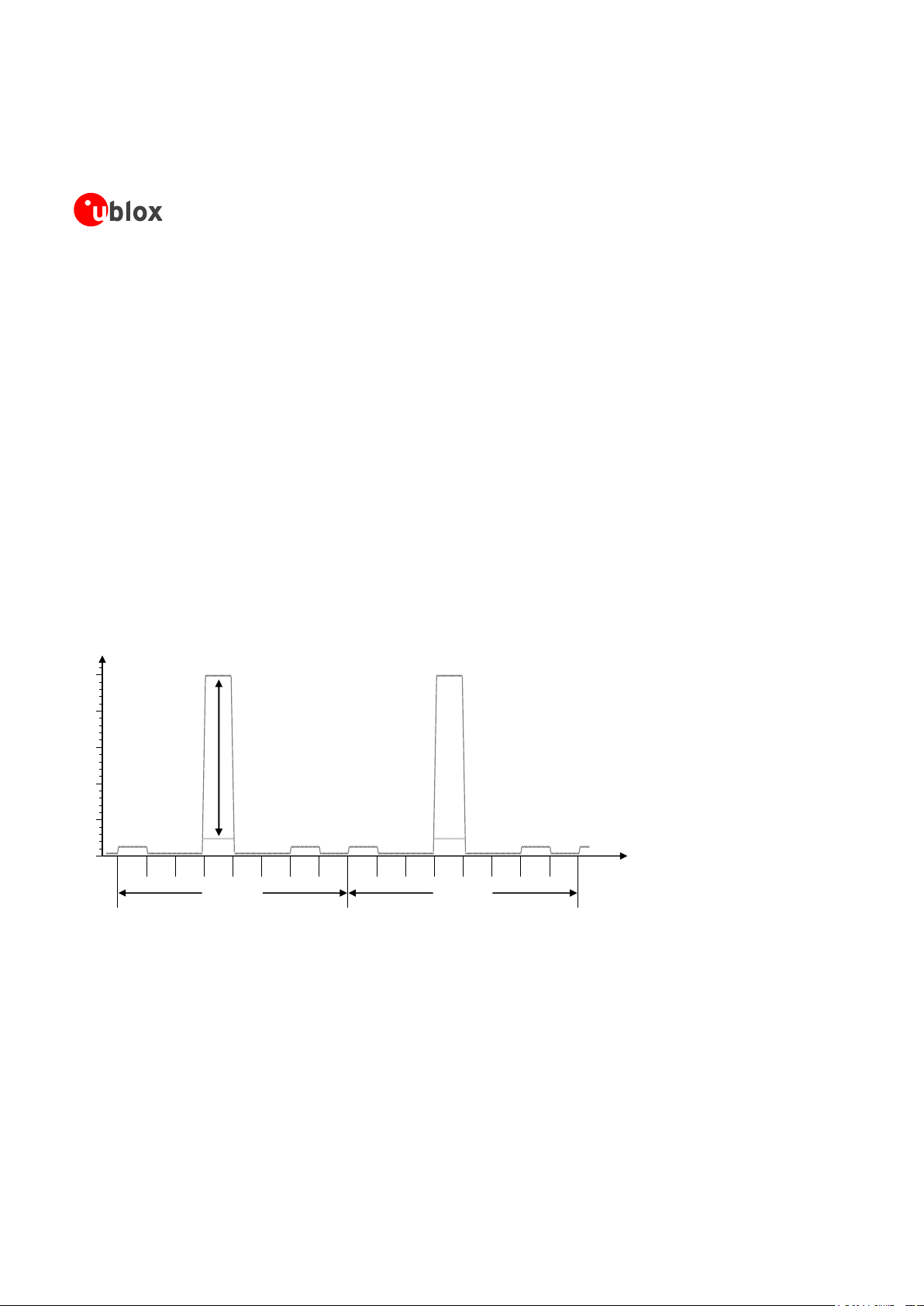
LISA-U2 series - System Integration Manual
UBX-13001118 - R19 Early Production Information System description
Page 27 of 175
1.5.3 Current consumption profiles
During operation, the current drawn by the LISA-U2 series modules through the VCC pins can vary by several
orders of magnitude. This ranges from the high peak of current consumption during GSM transmitting bursts at
maximum power level in 2G connected mode, to continuous high current drawn in UMTS connected mode, to
the low current consumption during power saving in idle-mode.
1.5.3.1 2G connected mode
When a GSM call is established, the VCC consumption is determined by the current consumption profile typical
of the GSM transmitting and receiving bursts.
The current consumption peak during a transmission slot is strictly dependent on the transmitted power, which
is regulated by the network. If the module is transmitting in GSM talk mode in the GSM 850 or in the E-GSM
900 band and at the maximum RF power control level (approximately 2 W or 33 dBm in the allocated transmit
slot/burst) the current consumption can reach up to 2500 mA (with a highly unmatched antenna) for 576.9 µs
(width of the transmit slot/burst) with a periodicity of 4.615 ms (width of 1 frame = 8 slots/burst), so with a 1/8
duty cycle according to GSM TDMA (Time Division Multiple Access). If the module is in GSM connected mode in
the DCS 1800 or in the PCS 1900 band, the current consumption figures are lower than the one in the GSM 850
or in the E-GSM 900 band, due to 3GPP transmitter output power specifications (see LISA-U2 series Data
Sheet [1]).
During a GSM call, current consumption is in the order of 60-130 mA in receiving or in monitor bursts and is
about 10-40 mA in the inactive unused bursts (low current period). The more relevant contribution to determine
the average current consumption is set by the transmitted power in the transmit slot.
An example of current consumption profile of the data module in GSM talk mode is shown in Figure 11.
Time [ms]
RX
slot
unused
slot
unused
slot
TX
slot
unused
slot
unused
slot
MON
slot
unused
slot
RX
slot
unused
slot
unused
slot
TX
slot
unused
slot
unused
slot
MON
slot
unused
slot
GSM frame
4.615 ms
(1 frame = 8 slots)
Current [A]
Peak current depends
on TX power and
actual antenna load
GSM frame
4.615 ms
(1 frame = 8 slots)
1.5
1.0
0.5
0.0
2.5
2.0
Figure 11: VCC current consumption profile versus time during a GSM call (1 TX slot, 1 RX slot)
Page 28
LISA-U2 series - System Integration Manual
UBX-13001118 - R19 Early Production Information System description
Page 28 of 175
When a GPRS connection is established there is a different VCC current consumption profile also determined by
the transmitting and receiving bursts. In contrast to a GSM call, during a GPRS connection more than one slot
can be used to transmit and/or more than one slot can be used to receive. The transmitted power depends on
network conditions, which set the peak current consumption, but following the GPRS specifications the
maximum transmitted RF power is reduced if more than one slot is used to transmit, so the maximum peak of
current consumption is not as high as can be in case of a GSM call.
If the module transmits in GPRS class 12 connected mode in the GSM 850 or in the E-GSM 900 band at the
maximum power control level, the current consumption can reach up to 1600 mA (with unmatched antenna).
This happens for 2.307 ms (width of the 4 transmit slots/bursts) with a periodicity of 4.615 ms (width of 1 frame
= 8 slots/bursts), so with a 1/2 duty cycle, according to GSM TDMA. If the module is in GPRS connected mode in
the DCS 1800 or in the PCS 1900 band, the current consumption figures are lower than in the GSM 850 or in
the E-GSM 900 band, due to 3GPP transmitter output power specifications (see LISA-U2 series Data Sheet [1]).
Figure 12 reports the current consumption profiles in GPRS class 12 connected mode, in the GSM 850 or in the
E-GSM 900 band, with 4 slots used to transmit and 1 slot used to receive.
Time [ms]
RX
slot
unused
slot
TX
slot
TX
slot
TX
slot
TX
slot
MON
slot
unused
slot
RX
slot
unused
slot
TX
slot
TX
slot
TX
slot
TX
slot
MON
slot
unused
slot
GSM frame
4.615 ms
(1 frame = 8 slots)
Current [A]
GSM frame
4.615 ms
(1 frame = 8 slots)
1.5
1.0
0.5
0.0
2.5
2.0
Peak current depends
on TX power and
actual antenna load
Figure 12: VCC current consumption profile versus time during a GPRS/EDGE connection (4TX slots, 1 RX slot)
In case of EDGE connections the VCC current consumption profile is very similar to the GPRS current profile, so
the image shown in Figure 12, representing the current consumption profile in GPRS class 12 connected mode,
is valid for the EDGE class 12 connected mode as well.
Page 29
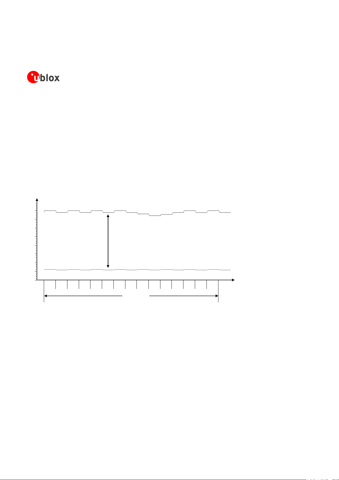
LISA-U2 series - System Integration Manual
UBX-13001118 - R19 Early Production Information System description
Page 29 of 175
1.5.3.2 3G connected mode
During a 3G connection, the module can transmit and receive continuously due to the Frequency Division Duplex
(FDD) mode of operation with the Wideband Code Division Multiple Access (WCDMA). The current consumption
depends again on output RF power, which is always regulated by network commands. These power control
commands are logically divided into a slot of 666 µs, thus the rate of power change can reach a maximum rate
of 1.5 kHz. There are no high current peaks as in the 2G connection, since transmission and reception are
continuously enabled due to FDD WCDMA implemented in the 3G that differs from the TDMA implemented in
the 2G case. In the worst scenario, corresponding to a continuous transmission and reception at maximum
output power (approximately 250 mW or 24 dBm), the current drawn by the module at the VCC pins is in the
order of continuous 500-800 mA (see LISA-U2 series Data Sheet [1] for detailed values). Even at lowest output
RF power (approximately 0.01 µW or -50 dBm), the current still remains in the order of 200 mA due to module
baseband processing and transceiver activity.
An example of current consumption profile of the data module in UMTS/HSxPA continuous transmission mode is
shown in Figure 13.
Time
[ms]
3G frame
10 ms
(1 frame = 15 slots)
Current [mA]
Current consumption
depends on TX power and
actual antenna load
170 mA
1 slot
666 µs
850 mA
0
300
200
100
500
400
600
700
800
Figure 13: VCC current consumption profile versus time during a UMTS/HSPA connection
When a packet data connection is established, the actual current profile depends on the amount of transmitted
packets; there might be some periods of inactivity between allocated slots where current consumption drops
about 100 mA. Alternatively, at higher data rates the transmitted power is likely to increase due to the higher
quality signal required by the network to cope with enhanced data speed.
Page 30
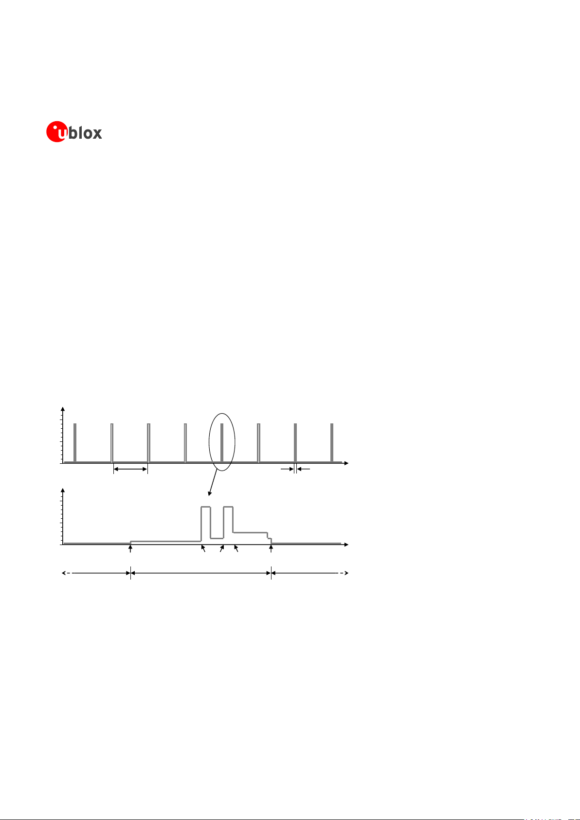
LISA-U2 series - System Integration Manual
UBX-13001118 - R19 Early Production Information System description
Page 30 of 175
1.5.3.3 2G and 3G cyclic idle/active mode (power saving enabled)
The power saving configuration is by default disabled, but it can be enabled using the appropriate AT command
(see the u-blox AT Commands Manual [2], AT+UPSV command). When power saving is enabled, the module
automatically enters idle-mode whenever possible.
When power saving is enabled, the module is registered or attached to a network and a voice or data call is not
enabled, the module automatically enters idle-mode whenever possible, but it must periodically monitor the
paging channel of the current base station (paging block reception), in accordance to GSM system requirements.
When the module monitors the paging channel, it wakes up to active mode, to enable the reception of paging
block. In between, the module switches to idle-mode. This is known as GSM discontinuous reception (DRX).
The module processor core is activated during the paging block reception, and automatically switches its
reference clock frequency from 32 kHz to the 26 MHz used in active-mode.
The time period between two paging block receptions is defined by the network (2G or 3G). This is the paging
period parameter, fixed by the base station through broadcast channel sent to all users on the same serving cell.
In case of 2G network, the time interval between two paging block receptions can be from 470.76 ms (DRX = 2,
i.e. width of 2 GSM multiframes = 2 x 51 GSM frames = 2 x 51 x 4.615 ms) up to 2118.42 ms (DRX = 9, i.e.
width of 9 GSM multiframes = 9 x 51 frames = 9 x 51 x 4.615 ms).
In case of 3G network, the principle is similar but time interval changes from 640 ms (DRX = 6, i.e. the width of
26 x 3G frames = 64 x 10 ms = 640 ms) up to 5120 ms (DRX = 9, i.e. width of 29 x 3G frames = 512 x 10 ms =
5120 ms).
An example of a module current consumption profile is shown in Figure 14: the module is registered with the
network (2G or 3G), automatically enters idle-mode and periodically wakes up to active mode to monitor the
paging channel for paging block reception.
20-30 ms
IDLE MODE ACTIVE MODE IDLE MODE
Active Mode
Enabled
Idle Mode
Enabled
2G case: 0.44-2.09 s
3G case: 0.61-5.09 s
IDLE MODE
20-30 ms
ACTIVE MODE
Time [s]
Current [mA]
100
50
0
Time [ms]
Current [mA]
100
50
0
RX
Enabled
DSP
Enabled
Figure 14: Description of VCC current consumption profile versus time when the module is registered with 2G or 3G networks:
the module is in idle-mode and periodically wakes up to active mode to monitor the paging channel for paging block reception
Page 31

LISA-U2 series - System Integration Manual
UBX-13001118 - R19 Early Production Information System description
Page 31 of 175
1.5.3.4 2G and 3G fixed active mode (power saving disabled)
Power saving configuration is by default disabled, or it can be disabled using the appropriate AT command (see
the u-blox AT Commands Manual [2], AT+UPSV command). When power saving is disabled, the module does
not automatically enter idle-mode whenever possible: the module remains in active mode.
The module processor core is activated during active-mode, and the 26 MHz reference clock frequency is used.
An example of the current consumption profile of the data module when power saving is disabled is shown in
Figure 15: the module is registered with the network, active-mode is maintained, and the receiver and the DSP
are periodically activated to monitor the paging channel for paging block reception.
ACTIVE MODE
2G case: 0.47-2.12 s
3G case: 0.64-5.12 s
Paging period
Time [s]
Current [mA]
100
50
0
Time [ms]
Current [mA]
100
50
0
RX
Enabled
DSP
Enabled
Figure 15: Description of the VCC current consumption profile versus time when power saving is disabled: the active-mode is
always held, and the receiver and the DSP are periodically activated to monitor the paging channel for paging block reception
Page 32

LISA-U2 series - System Integration Manual
UBX-13001118 - R19 Early Production Information System description
Page 32 of 175
1.5.4 RTC Supply (V_BCKP)
The V_BCKP pin connects the supply for the Real Time Clock (RTC) and Power-On / Reset internal logic. This
supply domain is internally generated by a linear regulator integrated in the Power Management Unit. The
output of this linear regulator is always enabled when the main voltage supply provided to the module through
VCC is within the valid operating range, with the module switched-off or powered-on.
V_BCKP supply output pin provides internal short circuit protection to limit start-up current and protect the
device in short circuit situations. No additional external short circuit protection is required.
Name
Description
Remarks
V_BCKP
Real Time Clock supply
V_BCKP output voltage = 1.8 V (typical)
Generated by the module to supply Real Time Clock when
VCC supply voltage is within valid operating range.
Table 12: Real Time Clock supply pin
The V_BCKP pin ESD sensitivity rating is 1 kV (Human Body Model according to JESD22-A114F). Higher
protection level could be required if the line is externally accessible on the application board. Higher
protection level can be achieved by mounting an ESD protection (e.g. EPCOS CA05P4S14THSG varistor
array) on the line connected to this pin, close to accessible point.
The RTC provides the time reference (date and time) of the module, also in power-off mode, when the V_BCKP
voltage is within its valid range (specified in the Input characteristics of Supply/Power pins table in LISA-U2 series
Data Sheet [1]). The RTC timing is normally used to set the wake-up interval during idle-mode periods between
network paging, but is able to provide programmable alarm functions by means of the internal 32.768 kHz
clock.
The RTC can be supplied from an external back-up battery through the V_BCKP, when the main voltage supply
is not provided to the module through VCC. This lets the time reference (date and time) run until the V_BCKP
voltage is within its valid range, even when the main supply is not provided to the module.
The RTC oscillator does not necessarily stop operation (i.e. the RTC counting does not necessarily stop) when
V_BCKP voltage value drops below the specified operating range minimum limit (1.00 V): the RTC value read
after a system restart could be not reliable, as explained in Table 13.
V_BCKP voltage value
RTC value reliability
Notes
1.00 V < V_BCKP < 1.90 V
RTC oscillator does not stop operation
RTC value read after a restart of the system is reliable
V_BCKP within operating range
0.05 V < V_BCKP < 1.00 V
RTC oscillator does not necessarily stop operation
RTC value read after a restart of the system is not reliable
V_BCKP below operating range
0.00 V < V_BCKP < 0.05 V
RTC oscillator stops operation
RTC value read after a restart of the system is reliable
V_BCKP below operating range
Table 13: RTC value reliability as function of V_BCKP voltage value
Consider that the module cannot switch on if a valid voltage is not present on VCC even when the RTC is
supplied through V_BCKP (meaning that VCC is mandatory to switch-on the module).
The RTC has very low power consumption, but is highly temperature dependent. For example at 25°C , with the
V_BCKP voltage equal to the typical output value, the power consumption is approximately 2 µA (see the Input
characteristics of Supply/Power pins table in the LISA-U2 series Data Sheet [1] for the detailed specification),
whereas at 70°C and an equal voltage the power consumption increases to 5-10 µA.
Page 33

LISA-U2 series - System Integration Manual
UBX-13001118 - R19 Early Production Information System description
Page 33 of 175
The internal regulator for V_BCKP is optimized for low leakage current and very light loads. It is not
recommended to use V_BCKP to supply external loads.
If V_BCKP is left unconnected and the module main voltage supply is removed from VCC, the RTC is supplied
from the bypass capacitor mounted inside the module. However, this capacitor is not able to provide a long
buffering time: within few milliseconds the voltage on V_BCKP will go below the valid range (1 V min). This has
no impact on cellular connectivity, as all the functionalities of the module do not rely on date and time setting.
Leave V_BCKP unconnected if the RTC is not required when the VCC supply is removed. The date and
time will not be updated when VCC is disconnected. If VCC is always supplied, then the internal regulator
is supplied from the main supply and there is no need for an external component on V_BCKP.
If RTC is required to run for a time interval of T [s] at 25°C when VCC supply is removed, place a capacitor with a
nominal capacitance of C [µF] at the V_BCKP pin. Choose the capacitor using the following formula:
C [µF] = (Current_Consumption [µA] x T [s]) / Voltage_Drop [V]
= 2.50 x T [s] for LISA-U2 series
For example, a 100 µF capacitor (such as the Murata GRM43SR60J107M) can be placed at V_BCKP to provide a
long buffering time. This capacitor will hold V_BCKP voltage within its valid range for around 50 s at 25°C, after
the VCC supply is removed. If a very long buffering time is required, a 70 mF super-capacitor (e.g. Seiko
Instruments XH414H-IV01E) can be placed at V_BCKP, with a 4.7 k series resistor to hold the V_BCKP voltage
within its valid range for approximately 10 hours at 25°C, after the VCC supply is removed. The purpose of the
series resistor is to limit the capacitor charging current due to the large capacitor specifications, and also to let a
fast rise time of the voltage value at the V_BCKP pin after VCC supply has been provided. These capacitors will
allow the time reference to run during battery disconnection.
LISA-U2 series
C1
(a)
2
V_BCKP
R2
LISA-U2 series
C2
(superCap)
(b)
2
V_BCKP
D3
LISA-U2 series
B3
(c)
2
V_BCKP
Figure 16: Real time clock supply (V_BCKP) application circuits: (a) using a 100 µF capacitor to let the RTC run for ~50 s after VCC
removal; (b) using a 70 mF capacitor to let RTC run for ~10 hours after VCC removal; (c) using a non-rechargeable battery
Reference
Description
Part Number - Manufacturer
C1
100 µF Tantalum Capacitor
GRM43SR60J107M - Murata
R2
4.7 kΩ Resistor 0402 5% 0.1 W
RC0402JR-074K7L - Yageo Phycomp
C2
70 mF Capacitor
XH414H-IV01E - Seiko Instruments
Table 14: Example of components for V_BCKP buffering
If longer buffering time is required to allow the time reference to run during a disconnection of the VCC supply,
then an external battery can be connected to V_BCKP pin. The battery should be able to provide a proper
nominal voltage and must never exceed the maximum operating voltage for V_BCKP (specified in the Input
characteristics of Supply/Power pins table in LISA-U2 series Data Sheet [1]). The connection of the battery to
V_BCKP should be done with a suitable series resistor for a rechargeable battery, or with an appropriate series
diode for a non-rechargeable battery. The purpose of the series resistor is to limit the battery charging current
due to the battery specifications, and also to allow a fast rise time of the voltage value at the V_BCKP pin after
Page 34

LISA-U2 series - System Integration Manual
UBX-13001118 - R19 Early Production Information System description
Page 34 of 175
the VCC supply has been provided. The purpose of the series diode is to avoid a current flow from the module
V_BCKP pin to the non-rechargeable battery.
Combining a LISA-U2 series cellular module with a u-blox GNSS receiver, the VCC supply of the GNSS receiver is
controlled by the cellular module by means of the “GNSS supply enable” function provided by the GPIO2 of the
cellular module. In this case the V_BCKP supply output of the LISA-U2 series cellular module can be connected
to the V_BCKP backup supply input pin of the GNSS receiver to provide the supply for the GNSS real time clock
and backup RAM when the VCC supply of the cellular module is within its operating range and the VCC supply
of the GNSS receiver is disabled. This enables the u-blox GNSS receiver to recover from a power breakdown with
either a hotstart or a warmstart (depending on the duration of the GNSS VCC outage) and to maintain the
configuration settings saved in the backup RAM. See the section 1.10 for more details regarding the application
circuit with a u-blox GNSS receiver.
Page 35

LISA-U2 series - System Integration Manual
UBX-13001118 - R19 Early Production Information System description
Page 35 of 175
1.5.5 Interface supply (V_INT)
The same voltage domain used internally to supply the digital interfaces is also available on the V_INT pin. The
internal regulator that generates the V_INT supply is a switching step down converter that is directly supplied
from VCC. The voltage regulator output is set to 1.8 V (typical) when the module is switched on and is disabled
when the module is switched off or when the RESET_N pin is forced the low level. The switching regulator
operates in Pulse Width Modulation (PWM) for high output current mode but automatically switches to Pulse
Frequency Modulation (PFM) at low output loads for greater efficiency, e.g. when the module is in idle-mode
between paging periods.
V_INT supply output pin provides internal short circuit protection to limit start -up current and protect the device
in short circuit situations. No additional external short circuit protection is required.
Name
Description
Remarks
V_INT
Digital Interfaces supply output
V_INT = 1.8V (typical) generated by the module when it is
switched-on and the RESET_N (external reset input pin) is
not forced to the low level.
V_INT is the internal supply for digital interfaces.
The user may draw limited current from this supply rail.
Table 15: Interface supply pin
The V_INT pin ESD sensitivity rating is 1 kV (Human Body Model according to JESD22-A114F). Higher
protection level could be required if the line is externally accessible on the application board. Higher
protection level can be achieved by mounting an ESD protection (e.g. EPCOS CA05P4S14THSG varistor
array) on the line connected to this pin, close to accessible point.
Since it supplies internal digital circuits (see Figure 3), V_INT is not suited to directly supply any sensitive analog
circuit: the voltage ripple can range from 15 mVpp during active mode (PWM), to 70 mVpp in idle-mode (PFM).
V_INT can be used to supply external digital circuits operating at the same voltage level as the digital
interface pins, i.e. 1.8 V (typical). It is not recommended to supply analog circuitry without adequate
filtering for digital noise.
Do not apply loads which might exceed the limit for maximum available current from V_INT supply, as
this can cause malfunctions in internal circuitry supplies to the same domain. The detailed electrical
characteristics are described in LISA-U2 series Data Sheet [1].
V_INT can only be used as an output; do not connect any external regulator on V_INT. If not used, this
pin should be left unconnected.
The V_INT digital interfaces supply output is mainly used to:
Pull-up DDC (I
2
C) interface signals (see section 1.10.2 for more details)
Pull-up SIM detection signal (see section 1.8 for more details)
Supply voltage translators to connect digital interfaces of the module to a 3.0 V device (see sections 1.9.2.4,
1.9.4.4 for more details)
Supply a 1.8 V u-blox 6 or subsequent GNSS receiver (see section 1.10.2 for more details)
Indicate when the module is switched on and the RESET_N external hardware reset input is not forced low
(see sections 1.6.1.5, 1.6.2 and 1.6.3 for more details)
Page 36

LISA-U2 series - System Integration Manual
UBX-13001118 - R19 Early Production Information System description
Page 36 of 175
1.6 System functions
1.6.1 Module power-on
When the LISA-U2 series modules are in the not-powered mode (i.e. switched off with the VCC module supply
not applied), they can be switched on by:
Rising edge on the VCC pin to a valid voltage as module supply (i.e. applying module supply)
Alternately, the RESET_N pin can be held to the low level during the VCC rising edge, so that the module
switches on releasing the RESET_N pin when the VCC module supply voltage stabilizes at its proper nominal
value within the normal operating range
The status of the PWR_ON input pin of LISA-U2 series modules while applying the VCC module supply is not
relevant: during this phase the PWR_ON pin can be set high or low by the external circuit.
When the LISA-U2 series modules are in the power-off mode (i.e. switched off by means of the AT+CPWROFF
command, with valid VCC module supply applied), they can be switched on by:
Low pulse on the PWR_ON pin (i.e. forcing to the low level the pin normally high by external pull-up)
Rising edge on the RESET_N pin (i.e. releasing from low level the pin, normally high by internal pull-up)
RTC alarm (i.e. pre-programmed scheduled time by AT+CALA command)
Name
Description
Remarks
PWR_ON
Power-on input
PWR_ON pin has high input impedance.
Do not keep floating in noisy environment: external pull-up
required.
Table 16: Power-on pin
The PWR_ON pin ESD sensitivity rating is 1 kV (Human Body Model according to JESD22-A114F). Higher
protection level could be required if the line is externally accessible on the application board. Higher
protection level can be achieved by mounting an ESD protection (e.g. EPCOS CA05P4S14THSG varistor
array) on the line connected to this pin, close to accessible point.
1.6.1.1 Rising edge on VCC
Applying a proper supply to VCC pins, the module supply supervision circuit controls the subsequent activation
of the power up state machines: the module is switched on when the voltage rises up to the VCC normal
operating range minimum limit starting from a voltage value lower than 2.25 V (see LISA-U2 series Data
Sheet [1] for the VCC normal operating range minimum limit).
The voltage at VCC pins must ramp from 2.5 V to 3.2 V within 1 ms to properly switch on the module.
If the external supply circuit is not able to provide this VCC voltage slope, keep the RESET_N input low
during the VCC rising edge, so that the module switches on, releasing the RESET_N pin when the VCC
voltage stabilizes at its nominal value within the normal operating range.
The status of the PWR_ON input pin during the VCC apply phase is not relevant: LISA-U2 modules switch on
when a proper rising edge on the VCC pin is applied, during this phase the PWR_ON pin can be set high or low
by the external circuit.
Page 37

LISA-U2 series - System Integration Manual
UBX-13001118 - R19 Early Production Information System description
Page 37 of 175
1.6.1.2 Low pulse on PWR_ON
When the module is in power-off mode, i.e. it has been properly switched off as described in the section 1.6.2
(e.g. by the AT+CPWROFF command) and a voltage within the operating range is maintained at the VCC pins,
the module can be switched on by means of the PWR_ON input pin: a falling edge must be provided on the
PWR_ON pin, which must be then held low for an appropriate time period as specified in LISA-U2 series Data
Sheet [1].
The electrical characteristics of the PWR_ON input pin are different from the other digital I/O interfaces; the
detailed electrical characteristics are described in LISA-U2 series Data Sheet [1].
The PWR_ON pin has high input impedance and is weakly pulled to the high level on the module. Avoid
keeping it floating in a noisy environment. To hold the high logic level stable, the PWR_ON pin must be
connected to a pull-up resistor (e.g. 100 kΩ) biased by the V_BCKP supply pin of the module.
Following are some typical examples of application circuits to turn the module on using the PWR_ON input pin.
Connecting the PWR_ON input to an external device (e.g. application processor), use an open drain output on
the external device with an external pull-up resistor (e.g. 100 kΩ) biased by V_BCKP supply pin of the module.
A push-pull output of an application processor can also be used: in this case the pull-up can be used to pull the
PWR_ON level high when the application processor is switched off. If the high-level voltage of the push-pull
output pin of the application processor is greater than the maximum input voltage operating range of the
V_BCKP pin (see the V_BCKP Input characteristics of Supply/Power pins table in LISA-U2 series Data Sheet [1]),
the V_BCKP supply cannot be used to bias the pull-up resistor: the supply rail of the application processor or the
VCC supply could be used, but this will increase the V_BCKP (RTC supply) current consumption when the
module is in not-powered mode (VCC supply not present). Using a push-pull output of the external device, take
care to fix the proper level in all the possible scenarios to avoid an inappropriate switch-on of the module.
Open
Drain
Output
Application
processor
LISA-U2 series
Rext
2
V_BCKP
19
PWR_ON
Figure 17: PWR_ON application circuits using an open drain output of an application processor
Reference
Description
Remarks
Rext
100 kΩ Resistor 0402 5% 0.1 W
External pull-up resistor
Table 17: Example of pull-up resistor for the PWR_ON application circuit
Page 38

LISA-U2 series - System Integration Manual
UBX-13001118 - R19 Early Production Information System description
Page 38 of 175
1.6.1.3 Rising edge on RESET_N
When the module is in power-off mode (i.e. switched off with VCC maintained), the module can be switched on
by means of the RESET_N input pin alternatively to the PWR_ON input pin: the RESET_N signal must be forced
low for at least 50 ms and then released to generate a rising edge that starts the module power-on sequence.
RESET_N input pin can also be used to perform an “external” or “hardware” reset of the module, as described
in the section 1.6.3.
Electrical characteristics of the LISA-U2 series RESET_N input are slightly different from the other digital I/O
interfaces: the pin provides different input voltage thresholds. Detailed electrical characteristics are described in
LISA-U2 series Data Sheet [1].
RESET_N is pulled high to V_BCKP by an integrated pull-up resistor also when the module is in power-off
mode. Therefore an external pull-up is not required on the application board.
The simplest way to switch on the module by means of the RESET_N input pin is to use a push button that
shorts the RESET_N pin to ground: the module will be switched on at the release of the push button, since the
RESET_N will be forced to the high level by the integrated pull-up resistor, generating a rising edge.
If RESET_N is connected to an external device (e.g. an application processor on an application board) an open
drain output can be directly connected without any external pull-up. A push-pull output can be used too: in this
case make sure that the high level voltage of the push -pull circuit is below the maximum voltage operating
range of the RESET_N pin (specified in the RESET_N pin characteristics table in LISA-U2 series Data Sheet [1]).
To avoid unwanted power-on or reset of the module make sure to fix the proper level at the RESET_N input pin
in all possible scenarios.
Some typical examples of application circuits using the RESET_N input pin are described in the section 1.6.3.
1.6.1.4 Real Time Clock (RTC) alarm
When the module is in power-off mode (i.e. switched off with VCC maintained), it can be switched on by means
of an RTC alarm previously programmed (see the u-blox AT Commands Manual [2], AT+CALA command)
alternatively to the PWR_ON and RESET_N pins: the RTC system will initiate the power-on sequence.
1.6.1.5 Additional considerations
The module is switched on when the VCC voltage rises up to the normal operating range (i.e. applying supply
properly, as described in section 1.6.1.1): the module is commonly switched on in this way for the first time.
Then, the module must be properly switched off as described in section 1.6.2, e.g. by AT+CPWROFF command.
When the module is in power-off mode, i.e. it has been properly switched off as described in the section 1.6.2
(e.g. by the AT+CPWROFF command) and a voltage within the operating range is maintained at the VCC pins,
the module can be switched on by a proper start-up event (i.e. by PWR_ON as described in Figure 18 and
section 1.6.1.2, or by RESET_N as described in section 1.6.1.3, or by RTC alarm as described in section 1.6.1.4).
Page 39

LISA-U2 series - System Integration Manual
UBX-13001118 - R19 Early Production Information System description
Page 39 of 175
Figure 18 shows the modules power-on sequence from the power-off mode, describing the following phases:
The external supply is still applied to the VCC inputs as it is assumed that the module has been previously
switched off by means of the AT+CPWROFF command: the V_BCKP output is internally enabled as proper
VCC is present, the RESET_N of LISA-U2 series is set to high logic level due to internal pull-up to V_BCKP,
the PWR_ON is set to high logic level due to external pull-up connected to V_BCKP or VCC.
The PWR_ON input pin is set low for a valid time period, representing the start-up event.
All the generic digital pins of the modules are tri-stated until the switch-on of their supply source (V_INT):
any external signal connected to the generic digital pins must be tri-stated or set low at least until the
activation of the V_INT supply output to avoid latch-up of circuits and allow a proper boot of the module.
The V_INT generic digital interfaces supply output is enabled by the integrated power management unit.
The internal reset signal is held low by the integrated power management unit: the baseband processor core
and all the digital pins of the modules are held in reset state, which is reported for each pin of the module in
the pin description table of LISA-U2 series Data Sheet [1].
When the internal reset signal is released by the integrated power management unit, the processor core
starts to configure the digital pins of the modules to each default operational state.
The duration of these pins’ configuration phase differs within generic digital interfaces (3 s typical) and USB
interface due to specific host / device enumeration timings (5 s typical, see the section 1.9.3.1). The host
application processor should not send any AT command over the AT interfaces (USB, UART) of the modules
until the end of these interfaces’ configuration phase to allow a proper boot of the module.
After the interfaces’ configuration phase, the application can start sending AT commands, and the following
starting procedure is suggested to check the effective completion of the module internal boot sequence:
send AT and wait for the response with a 30 s timeout, iterate it 4 times without resetting or removing the
VCC supply of the module, and then run the application.
VCC
V_BCKP
PWR_ON
V_INT
Internal Rese t
System State
BB Pads State
Interna l Rese t → Ope rational Operational
Tristate / Floa ting
Interna l Rese t
OFF
ON
Start-up
event
0 ms
~35 ms
~3 s
PWR_ON
can be set high
Start of interface
configuration
Generic digital interface s
are configured
Figure 18: LISA-U2 series power-on sequence description
The Internal Reset signal is not available on a module pin, but the application can monitor the V_INT pin
to sense the start of the power-on sequence.
Any external signal connected to the UART interface, SPI/IPC interface, I
2
S interfaces and GPIOs must be
tri-stated when the module is in power-down mode, when the external reset is forced low and during the
module power-on sequence (at least for 3 s after the start-up event), to avoid latch-up of circuits and let a
proper boot of the module. If the external signals connected to the cellular module cannot be tri-stated,
insert a multi channel digital switch (e.g. Texas Instruments SN74CB3Q16244, TS5A3159, or TS5A63157)
between the two-circuit connections and set to high impedance during module power down mode, when
external reset is forced low and during power on sequence.
Page 40

LISA-U2 series - System Integration Manual
UBX-13001118 - R19 Early Production Information System description
Page 40 of 175
1.6.2 Module power-off
The power-off sequence of LISA-U2 series modules can be correctly started, so that the current parameter
settings are saved in the module’s non-volatile memory and a proper network detach is performed, in one of
these ways:
AT+CPWROFF command (more details in u-blox AT Commands Manual [2])
Low pulse on the PWR_ON pin for at least 1 s
An over-temperature or an under-temperature shutdown occurs when the temperature measured within the
cellular module reaches the dangerous area, if the optional Smart Temperature Supervisor feature is enabled and
configured by the dedicated AT command. For more details see the section 3.15 and to the u-blox AT
Commands Manual [2], +USTS AT command.
An abrupt under-voltage shutdown occurs on LISA-U2 modules when the VCC supply is removed, but in this
case the current parameter settings are not saved in the module’s non-volatile memory and a proper network
detach cannot be performed.
It is highly recommended to avoid an abrupt removal of the VCC supply: the power off sequence of the
module must be properly started as described above (e.g. by means of the AT+CPWROFF command), and
a proper VCC supply must be maintained at least until the end of the power off sequence, which occurs
when the generic digital interfaces supply output (V_INT) is switched off by the module.
An abrupt hardware shutdown occurs on LISA-U2 series modules when a low level is applied to the RESET_N
pin. In this case, the current parameter settings are not saved in the module’s non-volatile memory and a proper
network detach is not performed.
It is highly recommended to avoid an abrupt hardware shutdown of the module by forcing a low level on
the RESET_N input pin during module normal operation: the RESET_N line should be set low only if reset
or shutdown via AT commands fails or if the module does not reply to a specific AT command after a time
period longer than the one defined in the u-blox AT Commands Manual [2].
Page 41

LISA-U2 series - System Integration Manual
UBX-13001118 - R19 Early Production Information System description
Page 41 of 175
Figure 19 describes the module’s power-off sequence, properly started by sending the AT+CPWROFF command,
allowing storage of current parameter settings in the module’s non-volatile memory and a proper network
detach:
When the +CPWROFF AT command is sent, the module starts the switch-off routine.
The module replies OK on the AT interface: the switch-off routine is in progress.
At the end of the switch-off routine, all the digital pins are tri-stated and all the internal voltage regulators
are turned off, including the generic digital interfaces supply (V_INT), except the RTC supply (V_BCKP).
Then, the module remains in power-off mode as long as a switch on event does not occur (e.g. applying a
proper low level to the PWR_ON input, or applying a proper low level to the RESET_N input), and enters
not-powered mode if the supply is removed from the VCC pins.
VCC
V_BCKP
PWR_ON
RESET_N
V_INT
Internal Reset
System State
BB Pins State Operational
OFF
Tristate / Floa ting
ON
Operational → Tristate
AT+CP WROFF
sent to the module
OK
replied by the module
VCC
can be removed
Figure 19: LISA-U2 series Power-off sequence description
The Internal Reset signal is not available on a module pin, but the application can monitor the V_INT pin
to sense the end of the LISA-U2 series power-off sequence.
The duration of each phase in the LISA-U2 series modules’ switch-off routines can largely vary from the
values reported in Figure 19 (e.g. from tens of milliseconds up to tens of seconds), depending on the
application / network settings and the concurrent module activities.
If the AT command +CPWROFF is issued to switch off the module over a multiplexer channel, the
completion of the module power-off sequence could require additionally up to 2.5 s, after the module OK
reply. Therefore, if the Application Processor (AP) controls the VCC supply of the module, the AP should
disable the multiplexer protocol and then issue the AT+CPWROFF command over the used AT interface,
or otherwise the AP should issue the AT+CPWROFF command over a multiplexer channel and wait
additionally 2.5 s after OK reception before removing the module VCC supply.
Tristated pins are always subject to floating caused by noise: to prevent unwanted effects, fix them with
proper pull-up or pull down resistors to stable voltage rails to fix their level when the module is in Power
down state.
Any external signal connected to the UART interface, SPI/IPC interface, I
2
S interfaces and GPIOs must be
tri-stated when the module is in power-down mode, when the external reset is forced low and during the
module power-on sequence (at least for 3 s after the start-up event), to avoid latch-up of circuits and
allow a proper boot of the module. If the external signals connected to the cellular module cannot be tristated, insert a multi channel digital switch (e.g. Texas Instruments SN74CB3Q16244, TS5A3159, or
TS5A63157) between the two-circuit connections and set to high impedance during module power down
mode, when external reset is forced low and during power-on sequence.
Page 42

LISA-U2 series - System Integration Manual
UBX-13001118 - R19 Early Production Information System description
Page 42 of 175
1.6.3 Module reset
LISA-U2 series modules can be properly reset (rebooted) by:
AT+CFUN command (see the u-blox AT Commands Manual [2] for more details).
This command causes an “internal” or “software” reset of the module, causing an asynchronous reset of the
module baseband processor, excluding the integrated Power Management Unit and the RTC internal block. The
V_INT interfaces supply is enabled and each digital pin is set in its internal reset state (reported in the pin
description table in LISA-U2 series Data Sheet [1]), the V_BCKP supply and the RTC block are enabled.
Forcing an “internal” or “software” reset, the current parameter settings are saved in the module’s non -volatile
memory and a proper network detach is performed: this is the proper way to reset the modules.
An abrupt hardware reset occurs on LISA-U2 series modules when a low level is applied on the RESET_N input
pin for a specific time period. In this case, the current parameter settings are not saved in the module’s
non-volatile memory and a proper network detach is not performed.
It is highly recommended to avoid an abrupt “external” or “hardware” reset of the module by forcing a
low level on the RESET_N input pin during the module normal operation: the RESET_N line should be set
low only if reset or shutdown via AT commands fails or if the module does not provide a reply to a specific
AT command after a time period longer than the one defined in the u-blox AT Commands Manual [2].
When a low level is applied to the RESET_N input, it causes an “external” or “hardware” reset of the module,
with an asynchronous abrupt reset of the entire module, including the integrated Power Management Unit,
except for the RTC internal block. The V_INT interfaces supply is switched off and all the digital pins of the
modules are tri-stated, but the V_BCKP supply and the RTC block are enabled.
Forcing an “external” or “hardware” reset, the current parameter settings are not saved in the module’s
non-volatile memory and a proper network detach is not performed.
When RESET_N is released from the low level, the module automatically starts its power-on sequence from the
reset state. The same procedure is followed for the module reset via AT command after having performed the
network detach and the parameter saving in non-volatile memory.
Name
Description
Remarks
RESET_N
External reset input
Internal 10 k pull-up to V_BCKP
Table 18: Reset pin
The RESET_N pin ESD sensitivity rating is 1 kV (Human Body Model according to JESD22-A114F). Higher
protection level could be required if the line is externally accessible on the application board. Higher
protection level can be achieved by mounting an ESD protection (e.g. EPCOS CA05P4S14THSG varistor
array) on the line connected to this pin, close to accessible point.
For more details about RESET_N circuit precautions for ESD immunity, see section 2.5.3.
The electrical characteristics of RESET_N are different from the other digital I/O interfaces. The detailed electrical
characteristics are described in LISA-U2 series Data Sheet [1].
RESET_N is pulled high by an integrated 10 k pull-up resistor to V_BCKP. Therefore an external pull-up is not
required on the application board.
Following are some typical examples of application circuits using the RESET_N input pin.
The simplest way to reset the module is to use a push button that shorts the RESET_N pin to ground.
Page 43

LISA-U2 series - System Integration Manual
UBX-13001118 - R19 Early Production Information System description
Page 43 of 175
If RESET_N is connected to an external device (e.g. an application processor on an application board) an open
drain output can be directly connected without any external pull-up. A push-pull output can be used too: in this
case make sure that the high level voltage of the push-pull circuit is below the maximum voltage operating
range of the RESET_N pin (specified in the RESET_N pin characteristics table in LISA-U2 series Data Sheet [1]).
To avoid unwanted reset of the module make sure to fix the proper level at the RESET_N input pin in all possible
scenarios.
As ESD immunity test precaution, a 47 pF bypass capacitor (e.g. Murata GRM1555C1H470JA01), a proper series
chip ferrite bead noise/EMI suppression filter (e.g. Murata BLM15HD182SN1) and a 220 nF bypass capacitor (e.g.
Murata GRM155R60J224KE01) must be added as close as possible to the RESET_N pin of LISA-U2 series
modules to avoid a module reset caused by an electrostatic discharge applied to the application board (for more
details, see section 2.5.3).
LISA-U2 series
2
V_BCKP
22
RESET_N
Reset
push button
ESD
Open
Drain
Output
Application
processor
LISA-U2 series
2
V_BCKP
22
RESET_N
Rint
Rint
EMI1
C1
EMI2
C3
C2
C4
Figure 20: RESET_N application circuits using a push button and an open drain output of an application processor
Reference
Description
Remarks
ESD
Varistor for ESD protection.
CT0402S14AHSG - EPCOS
C1, C3
47 pF Capacitor Ceramic C0G 0402 5% 50 V
GRM1555C1H470JA01 - Murata
C2, C4
220 nF Capacitor Ceramic X5R 0402 10% 6.3 V
GRM155R60J224KE01 - Murata
EMI1, EMI2
Chip Ferrite Bead Noise/EMI Suppression Filter
1800 Ω at 100 MHz, 2700 Ω at 1 GHz
BLM15HD182SN1 - Murata
Rint
10 kΩ Resistor 0402 5% 0.1 W
Internal pull-up resistor
Table 19: Example of ESD protection components for the RESET_N application circuit
Any external signal connected to the UART interface, SPI/IPC interface, I
2
S interfaces and GPIOs must be
tri-stated when the module is in power-down mode, when the external reset is forced low and during the
module power-on sequence (at least for 3 s after the start-up event), to avoid latch-up of circuits and
allow a proper boot of the module. If the external signals connected to the cellular module cannot be tristated, insert a multi channel digital switch (e.g. Texas Instruments SN74CB3Q16244, TS5A3159, or
TS5A63157) between the two-circuit connections and set to high impedance during module power down
mode, when external reset is forced low and during power-on sequence.
Page 44

LISA-U2 series - System Integration Manual
UBX-13001118 - R19 Early Production Information System description
Page 44 of 175
1.7 RF connection
The ANT pin, provided by all LISA-U2 modules, represents the main RF input/output used to transmit and receive
the 2G and 3G RF signal: the main antenna must be connected to this pad. The ANT pin has a nominal
characteristic impedance of 50 and must be connected to the antenna through a 50 transmission line to
allow transmission and reception of radio frequency (RF) signals in the 2G and 3G operating bands.
The ANT_DIV pin, provided by LISA-U230 modules, represents the RF input for the integrated diversity receiver
implemented for both 2G and 3G cases: the antenna for the Rx diversity must be connected to this pad. The
ANT_DIV pin has a nominal characteristic impedance of 50 and must be connected to the antenna for the Rx
diversity through a 50 transmission line to allow reception of radio frequency (RF) signals, improving the
cellular link quality and reliability on all 2G and 3G operating bands except the 2G DCS 1800.
Name
Module
Description
Remarks
ANT
All
RF input/output for main Tx/Rx antenna
Zo = 50 nominal characteristic impedance.
ANT_DIV
LISA-U230
RF input for Rx diversity antenna
Zo = 50 nominal characteristic impedance.
Table 20: Antenna pins
ESD immunity rating of ANT port is 1000 V (according to IEC 61000-4-2). Higher protection level could be
required if the line is externally accessible on the application board (for further details see section 2.5.3).
Choose an antenna with optimal radiating characteristics for the best electrical performance and overall module
functionality. An internal antenna, integrated on the application board, or an external antenna, connected to the
application board through a proper 50 connector, can be used. See section 2.4 and section 2.2.1.1 for further
details regarding antenna guidelines.
The recommendations of the antenna producer for correct installation and deployment (PCB
layout and matching circuitry) must be followed.
If an external antenna is used, the PCB-to-RF-cable transition must be implemented using either a suitable 50
connector, or an RF-signal solder pad (including GND) that is optimized for 50 characteristic impedance.
If antenna supervisor functionality is required, the main antenna connected to the ANT pin should have a built in
DC diagnostic resistor to ground to get proper detection functionality (See section 2.4.4).
Connect the Rx diversity antenna to the ANT_DIV pin of LISA-U230 modules unless the 2G and 3G Rx
diversity feature is disabled by AT command (see the u-blox AT Commands Manual [2], +URXDIV
command). The same pin (74) is marked RSVD (reserved) on the other modules that do not implement Rx
diversity: in this case the RSVD pin can be left unconnected.
Page 45

LISA-U2 series - System Integration Manual
UBX-13001118 - R19 Early Production Information System description
Page 45 of 175
1.8 (U)SIM interface
High-speed SIM/ME interface is implemented as well as automatic detection of the required SIM supporting
voltage.
Both 1.8 V and 3 V SIM types are supported: activation and deactivation with automatic voltage switch from
1.8 V to 3 V is implemented, according to ISO-IEC 7816-3 specifications. The SIM driver supports the PPS
(Protocol and Parameter Selection) procedure for baud-rate selection, according to the values determined by the
SIM Card.
The VSIM supply output pin provides internal short circuit protection to limit start-up current and protect the
device in short circuit situations. No additional external short circuit protection is required.
Name
Description
Remarks
VSIM
SIM supply
1.80 V typical or 2.90 V typical
Automatically generated by the module
SIM_CLK
SIM clock
3.25 MHz clock frequency
SIM_IO
SIM data
Open drain, internal 4.7 k pull-up resistor to VSIM
SIM_RST
SIM reset
Table 21: SIM Interface pins
A low capacitance (i.e. less than 10 pF) ESD protection (e.g. Infineon ESD8V0L2B-03L or AVX USB0002RP)
must be placed near the SIM card holder on each line (VSIM, SIM_IO, SIM_CLK, SIM_RST). The SIM
interface pins ESD sensitivity rating is 1 kV (Human Body Model according to JESD22-A114F): higher
protection level is required if the lines are connected to an SIM card connector, since they are externally
accessible on the application board.
For more details about the general precautions for ESD immunity about SIM interface pins, see section
2.5.3.
The following SIM services are supported:
Abbreviated Dialing Numbers (ADN)
Fixed Dialing Numbers (FDN)
Last Dialed Numbers (LDN)
Service Dialing Numbers (SDN)
SIM Application Toolkit and USIM Application Toolkit (USAT) are supported.
The GPIO5 pin is configured as an external interrupt to detect the SIM card mechanical / physical presence. The
pin is configured as input with an internal active pull-down enabled, and it can sense SIM card presence only if
properly connected to the mechanical switch of a SIM card holder as described in section 1.8.1.4 and 1.8.1.5:
Low logic level at GPIO5 input pin is recognized as SIM card not present
High logic level at GPIO5 input pin is recognized as SIM card present
The SIM card detection function provided by GPIO5 pin is an optional feature that can be implemented / used or
not according to the application requirements. An Unsolicited Result Code (URC) can be generated each time
that there is a change of status (for more details see the “simind” value of the <descr> parameter of +CIND and
+CMER commands in the u-blox AT Commands Manual [2]).
All the LISA-U2 series modules provide the additional function “SIM card hot insertion/removal” on the GPIO5
pin, which can be enabled using the AT+UDCONF=50 command.
For more details on SIM detection function see section 1.12 as well as the u-blox AT Commands Manual [2],
+UGPIOC, +UDCONF=50 commands.
Page 46

LISA-U2 series - System Integration Manual
UBX-13001118 - R19 Early Production Information System description
Page 46 of 175
1.8.1 (U)SIM application circuits
1.8.1.1 SIM cards, SIM connectors and SIM chips selection
The ISO/IEC 7816, the ETSI TS 102 221 and the ETSI TS 102 671 specifications define the physical, electrical and
functional characteristics of Universal Integrated Circuit Cards (UICC) which contains the Subscriber Identification
Module (SIM) integrated circuit that securely stores all the information needed to identify and authenticate
subscribers over the GSM network.
Removable UICC / SIM card contacts mapping is defined by ISO/IEC 7816 and ETSI TS 102 221as follows:
Contact C1 = VCC (Supply) It must be connected to VSIM
Contact C2 = RST (Reset) It must be connected to SIM_RST
Contact C3 = CLK (Clock) It must be connected to SIM_CLK
Contact C4 = AUX1 (Auxiliary contact) It must be left not connected
Contact C5 = GND (Ground) It must be connected to GND
Contact C6 = VPP (Programming supply) It must be connected to VSIM
Contact C7 = I/O (Data input/output) It must be connected to SIM_IO
Contact C8 = AUX2 (Auxiliary contact) It must be left not connected
A removable SIM card can have 6 contacts (C1 = VCC, C2 = RST, C3 = CLK, C5 = GND, C6 = VPP, C7 = I/O) or
8 contacts, providing also the auxiliary contacts C4 = AUX1 and C8 = AUX2 for USB interfaces and other uses.
Only 6 contacts are required and must be connected to the module SIM card interface as described above , since
LISA-U2 modules do not support the additional auxiliary features (contacts C4 = AUX1 and C8 = AUX2).
Removable SIM cards are suitable for applications where the SIM changing is required during the product
lifetime.
A SIM card holder can have 6 or 8 positions if a mechanical card presence detector is not provided, or it can
have 6+2 or 8+2 positions if two additional pins corresponding to the normally-open mechanical switch
integrated in the SIM connector for the mechanical card presence detection a re provided: select a SIM connector
providing 6+2 or 8+2 positions if the optional SIM detection feature is required by the custom application,
otherwise a connector without integrated mechanical presence switch can be selected.
Solderable UICC / SIM chip contacts mapping (M2M UICC Form Factor) is defined by ETSI TS 102 671 as follows:
Package Pin 8 = UICC Contact C1 = VCC (Supply) It must be connected to VSIM
Package Pin 7 = UICC Contact C2 = RST (Reset) It must be connected to SIM_RST
Package Pin 6 = UICC Contact C3 = CLK (Clock) It must be connected to SIM_CLK
Package Pin 5 = UICC Contact C4 = AUX1 (Auxiliary contact) It must be left not connected
Package Pin 1 = UICC Contact C5 = GND (Ground) It must be connected to GND
Package Pin 2 = UICC Contact C6 = VPP (Programming supply) It must be connected to VSIM
Package Pin 3 = UICC Contact C7 = I/O (Data input/output) It must be connected to SIM_IO
Package Pin 4 = UICC Contact C8 = AUX2 (Auxiliary contact) It must be left not connected
A solderable SIM chip has 8 contacts and can provide also the auxiliary contacts C4 = AUX1 and C8 = AUX2 for
USB interfaces and other uses, but only 6 contacts are required and must be connected to the module SIM card
interface as described above, since LISA-U2 modules do not support the additional auxiliary features (contacts C4
= AUX1 and C8 = AUX2).
Solderable SIM chips are suitable for M2M applications where it is not required to change the SIM once installed.
Page 47

LISA-U2 series - System Integration Manual
UBX-13001118 - R19 Early Production Information System description
Page 47 of 175
1.8.1.2 Single SIM card without detection
A removable SIM card placed in a SIM card holder must be connected to the SIM card interface of LISA-U2
modules as described in Figure 21, where the optional SIM detection feature is not implemented (see the circuit
described in Figure 23 if the SIM detection feature is required).
Follow these guidelines connecting the module to a SIM connector without the SIM presence detection:
Connect the UICC / SIM contacts C1 (VCC) and C6 (VPP) to the VSIM pin of the module
Connect the UICC / SIM contact C7 (I/O) to the SIM_IO pin of the module
Connect the UICC / SIM contact C3 (CLK) to the SIM_CLK pin of the module
Connect the UICC / SIM contact C2 (RST) to the SIM_RST pin of the module
Connect the UICC / SIM contact C5 (GND) to ground
Provide a 100 nF bypass capacitor (e.g. Murata GRM155R71C104K) at the SIM supply line (VSIM), close to
the corresponding pad of the SIM connector, to prevent digital noise
Provide a bypass capacitor of about 22 pF to 47 pF (e.g. Murata GRM1555C1H330J) on each SIM line
(VSIM, SIM_CLK, SIM_IO, SIM_RST), very close to each specific pad of the SIM connector, to prevent RF
coupling especially in case the RF antenna is placed closer than 10 - 30 cm from the SIM card holder
Provide a very low capacitance (i.e. less than 10 pF) ESD protection (e.g. Tyco Electronics PESD0402-140) on
each externally accessible SIM line, close to each specific pad of the SIM connector: ESD sensitivity rating of
the SIM interface pins is 1 kV (Human Body Model according to JESD22-A114), so that, according to the
EMC/ESD requirements of the custom application, higher protection level can be required if the lines are
externally accessible on the application device
Limit capacitance and series resistance on each SIM signal (SIM_CLK, SIM_IO, SIM_RST) to match the
requirements for the SIM interface (27.7 ns is the maximum allowed rise time on the SIM_CLK line, 1.0 µs is
the maximum allowed rise time on the SIM_IO and SIM_RST lines)
LISA-U2 series
50
VSIM
48
SIM_IO
47
SIM_CLK
49
SIM_RST
4
V_INT
51
GPIO5
SIM CARD
HOLDER
C5C6C
7
C1C2C
3
SIM Card
Bottom View
(contacts side)
C1
VPP (C6)
VCC (C1)
IO (C7)
CLK (C3)
RST (C2)
GND (C5)
C2 C3 C5
J1
C4
D1 D2 D3 D4
C
8
C
4
Figure 21: Application circuit for the connection to a single removable SIM card, with SIM detection not implemented
Reference
Description
Part Number - Manufacturer
C1, C2, C3, C4
33 pF Capacitor Ceramic COG 0402 5% 25 V
GRM1555C1H330JZ01 - Murata
C5
100 nF Capacitor Ceramic X7R 0402 10% 16 V
GRM155R71C104KA01 - Murata
D1, D2, D3, D4
Very Low Capacitance ESD Protection
PESD0402-140 - Tyco Electronics
J1
SIM Card Holder
6 positions, without card presence switch
Various Manufacturers,
C707 10M006 136 2 - Amphenol
Table 22: Example of components for the connection to a single removable SIM card, with SIM detection not implemented
Page 48

LISA-U2 series - System Integration Manual
UBX-13001118 - R19 Early Production Information System description
Page 48 of 175
1.8.1.3 Single SIM chip
A solderable SIM chip (M2M UICC Form Factor) must be connected the SIM card interface of LISA-U2 modules
as described in Figure 22, where the optional SIM detection feature is not implemented (see the circuit described
in Figure 23 if the SIM detection feature is required).
Follow these guidelines connecting the module to a solderable SIM chip without the SIM presence detection:
Connect the UICC / SIM contacts C1 (VCC) and C6 (VPP) to the VSIM pin of the module
Connect the UICC / SIM contact C7 (I/O) to the SIM_IO pin of the module
Connect the UICC / SIM contact C3 (CLK) to the SIM_CLK pin of the module
Connect the UICC / SIM contact C2 (RST) to the SIM_RST pin of the module
Connect the UICC / SIM contact C5 (GND) to ground
Provide a 100 nF bypass capacitor (e.g. Murata GRM155R71C104K) at the SIM supply line (VSIM) close to
the specific pad of the SIM chip, to prevent digital noise
Provide a bypass capacitor of about 22 pF to 47 pF (e.g. Murata GRM1555C1H330J) on each SIM line
(VSIM, SIM_CLK, SIM_IO, SIM_RST), to prevent RF coupling especially in case the RF antenna is placed
closer than 10 - 30 cm from the SIM card holder
Limit capacitance and series resistance on each SIM signal (SIM_CLK, SIM_IO, SIM_RST) to match the
requirements for the SIM interface (27.7 ns is the maximum allowed rise time on the SIM_CLK line, 1.0 µs is
the maximum allowed rise time on the SIM_IO and SIM_RST lines)
LISA-U2 series
50
VSIM
48
SIM_IO
47
SIM_CLK
49
SIM_RST
4
V_INT
51
GPIO5
SIM CHIP
SIM Chip
Bottom View
(contacts side)
C1
VPP (C6)
VCC (C1)
IO (C7)
CLK (C3)
RST (C2)
GND (C5)
C2 C3 C5
U1
C4
2
8
3
6
7
1
C1 C5
C2 C6
C3 C7
C4 C8
8
7
6
5
1
2
3
4
Figure 22: Application circuit for the connection to a single solderable SIM chip, with SIM detection not implemented
Reference
Description
Part Number - Manufacturer
C1, C2, C3, C4
33 pF Capacitor Ceramic COG 0402 5% 25 V
GRM1555C1H330JZ01 - Murata
C5
100 nF Capacitor Ceramic X7R 0402 10% 16 V
GRM155R71C104KA01 - Murata
U1
SIM chip (M2M UICC Form Factor)
Various Manufacturers
Table 23: Example of components for the connection to a single solderable SIM chip, with SIM detection not implemented
1.8.1.4 Single SIM card with detection
A removable SIM card placed in a SIM card holder must be connected to the SIM card interface of LISA-U2
modules as described in Figure 23, where the optional SIM card detection feature is implemented so that the
module detects by means of the GPIO5 if a SIM card is present in the connector. The SW1 and SW2 pins of the
SIM card holder are connected to a normally-open mechanical switch integrated in the SIM connector. The
following cases are available:
SIM card not present: the GPIO5 signal is forced low by the pull-down resistor connected to ground (i.e. the
switch integrated in the SIM connector is open)
SIM card present: the GPIO5 signal is forced high by the pull-up resistor connected to V_INT (i.e. the switch
integrated in the SIM connector is closed)
Page 49

LISA-U2 series - System Integration Manual
UBX-13001118 - R19 Early Production Information System description
Page 49 of 175
Follow these guidelines connecting the module to a SIM connector implementing the SIM presence detection:
Connect the UICC / SIM contacts C1 (VCC) and C6 (VPP) to the VSIM pin of the module
Connect the UICC / SIM contact C7 (I/O) to the SIM_IO pin of the module
Connect the UICC / SIM contact C3 (CLK) to the SIM_CLK pin of the module
Connect the UICC / SIM contact C2 (RST) to the SIM_RST pin of the module
Connect the UICC / SIM contact C5 (GND) to ground
Connect one pin of the mechanical switch integrated in the SIM connector (e.g. the SW2 pin as described in
Figure 23) to the GPIO5 input pin of the module
Connect the other pin of the mechanical switch integrated in the SIM connector (e.g. the SW1 pin as
described in Figure 23) to the V_INT 1.8 V supply output of the module by means of a strong (e.g. 1 k)
pull-up resistor, as the R1 resistor in Figure 23
Provide a weak (e.g. 470 k) pull-down resistor at the SIM detection line, as the R2 resistor in Figure 23
Provide a 100 nF bypass capacitor (e.g. Murata GRM155R71C104K) at the SIM supply line (VSIM), close to
the specific pad of the SIM connector, to prevent digital noise
Provide a bypass capacitor of about 22 pF to 47 pF (e.g. Murata GRM1555C1H330J) on each SIM line
(VSIM, SIM_CLK, SIM_IO, SIM_RST), very close to each specific pad of the SIM connector, to prevent RF
coupling especially in case the RF antenna is placed closer than 10 - 30 cm from the SIM card holder
Provide a very low capacitance (i.e. less than 10 pF) ESD protection (e.g. Tyco Electronics PESD0402-140) on
each externally accessible SIM line, close to each specific pad of the SIM connector: ESD sensitivity rating of
the SIM interface pins is 1 kV (Human Body Model according to JESD22-A114), so that, according to the
EMC/ESD requirements of the custom application, higher protection level can be required if the lines are
externally accessible on the application device
Limit capacitance and series resistance on each SIM signal (SIM_CLK, SIM_IO, SIM_RST) to match the
requirements for the SIM interface (27.7 ns is the maximum allowed rise time on the SIM_CLK line, 1.0 µs is
the maximum allowed rise time on the SIM_IO and SIM_RST lines)
LISA-U2 series
50
VSIM
48
SIM_IO
47
SIM_CLK
49
SIM_RST
4
V_INT
51
GPIO5
SIM CARD
HOLDER
C5C6C
7
C1C2C
3
SIM Card
Bottom View
(contacts side)
C1
VPP (C6)
VCC (C1)
IO (C7)
CLK (C3)
RST (C2)
GND (C5)
C2 C3 C5
J1
C4
SW1
SW2
D1 D2 D3 D4 D5 D6
R2
R1
C
8
C
4
Figure 23: Application circuit for the connection to a single removable SIM card, with SIM detection implemented
Reference
Description
Part Number - Manufacturer
C1, C2, C3, C4
33 pF Capacitor Ceramic COG 0402 5% 25 V
GRM1555C1H330JZ01 - Murata
C5
100 nF Capacitor Ceramic X7R 0402 10% 16 V
GRM155R71C104KA01 - Murata
D1, D2, D3,
D4, D5, D6
Very Low Capacitance ESD Protection
PESD0402-140 - Tyco Electronics
R1
1 k Resistor 0402 5% 0.1 W
RC0402JR-071KL - Yageo Phycomp
R2
470 k Resistor 0402 5% 0.1 W
RC0402JR-07470KL- Yageo Phycomp
J1
SIM Card Holder
6 + 2 positions, with card presence switch
Various Manufacturers,
CCM03-3013LFT R102 - C&K Components
Table 24: Example of components for the connection to a single removable SIM card, with SIM detection implemented
Page 50

LISA-U2 series - System Integration Manual
UBX-13001118 - R19 Early Production Information System description
Page 50 of 175
1.8.1.5 Dual SIM card connection
Two SIM cards / chips can be connected to the module’s SIM interface, as described in the circuit of Figure 24.
LISA-U2 modules do not support the usage of two SIMs at the same time, but two SIMs can be populated on
the application board providing a proper switch to connect only the first SIM or only the second SIM per time to
the SIM interface of the modules as described in Figure 24.
All LISA-U2 series modules support SIM hot insertion / removal on the GPIO5 pin: if the feature is enabled using
the specific AT commands, the switch from first SIM to the second SIM can be properly done when a Low logic
level is present on the GPIO5 pin (‘SIM not inserted’ = SIM interface not enabled), without the necessity of a
module re-boot, so that the SIM interface will be re-enabled by the module to use the second SIM when an High
logic level will be re-applied on the GPIO5 pin. (For more details see section 1.12 and to the u-blox AT
Commands Manual [2], +UGPIOC, +UDCONF=50 commands.)
In the application circuit represented in Figure 24, the application processor will drive the SIM switch using its
own GPIO to properly select the SIM that is used by the module. Another GPIO may be used to handle the SIM
hot insertion / removal function of LISA-U2 series modules, which can also be handled by other external circuits
or by the cellular module GPIO according to the application requirements.
The dual SIM connection circuit described in Figure 24 can be implemented for SIM chips as well, providing
proper connection between SIM switch and SIM chip as described in Figure 22.
If it is required to switch between more than two SIMs, a circuit similar to the one described in Figure 24 can be
implemented: for example, in case of four SIM circuits, using a proper 4-pole 4-throw switch (or, alternatively,
four 1-pole 4-throw switches) instead of the suggested 4-pole 2-throw switch.
Follow these guidelines connecting the module to two SIM connectors:
Use a proper low on resistance (i.e. few ohms) and low on capacitance (i.e. few pF) 2-throw analog switch
(e.g. Fairchild FSA2567) as SIM switch to ensure high-speed data transfer according to SIM requirements.
Connect the contacts C1 (VCC) and C6 (VPP) of the two UICC / SIM to the VSIM pin of the module by
means of a proper 2-throw analog switch (e.g. Fairchild FSA2567).
Connect the contact C7 (I/O) of the two UICC / SIM to the SIM_IO pin of the module by means of a proper
2-throw analog switch (e.g. Fairchild FSA2567).
Connect the contact C3 (CLK) of the two UICC / SIM to the SIM_CLK pin of the module by means of a
proper 2-throw analog switch (e.g. Fairchild FSA2567).
Connect the contact C2 (RST) of the two UICC / SIM to the SIM_RST pin of the module by means of a
proper 2-throw analog switch (e.g. Fairchild FSA2567).
Connect the contact C5 (GND) of the two UICC / SIM to ground.
Provide a 100 nF bypass capacitor (e.g. Murata GRM155R71C104K) at the SIM supply line (VSIM), close to
the related pad of the two SIM connectors, to prevent digital noise.
Provide a bypass capacitor of about 22 pF to 47 pF (e.g. Murata GRM1555C1H470J) on each SIM line
(VSIM, SIM_CLK, SIM_IO, SIM_RST), very close to each related pad of the two SIM connectors, to prevent
RF coupling especially in case the RF antenna is placed closer than 10 - 30 cm from the SIM card holders.
Provide a very low capacitance (i.e. less than 10 pF) ESD protection (e.g. Tyco Electronics PESD0402-140) on
each externally accessible SIM line, close to each related pad of the two SIM connectors, according to the
EMC/ESD requirements of the custom application.
Limit capacitance and series resistance on each SIM signal (SIM_CLK, SIM_IO, SIM_RST) to match the
requirements for the SIM interface (27.7 ns is the maximum allowed rise time on the SIM_CLK line, 1.0 µs is
the maximum allowed rise time on the SIM_IO and SIM_RST lines).
Page 51

LISA-U2 series - System Integration Manual
UBX-13001118 - R19 Early Production Information System description
Page 51 of 175
LISA-U2 series
C1
FIRST
SIM CARD
VPP (C6)
VCC (C1)
IO (C7)
CLK (C3)
RST (C2)
GND (C5)
C2 C3 C5
J1
C4
D1 D2 D3 D4
GND
U1
50
VSIM
VSIM
1VSIM
2VSIM
VCC
C11
4PDT
Analog
Switch
3V8
48
SIM_IO
DAT
1DAT
2DAT
47
SIM_CLK
CLK
1CLK
2CLK
49
SIM_RST
RST
1RST
2RST
SEL
SECOND
SIM CARD
VPP (C6)
VCC (C1)
IO (C7)
CLK (C3)
RST (C2)
GND (C5)
J2
C6 C7 C8 C10
C9
D5 D6 D7 D8
Application
Processor
GPIO
R1
Figure 24: Application circuit for the connection to two removable SIM cards, with SIM detection implemented
Reference
Description
Part Number - Manufacturer
C1 – C4, C6 – C9
33 pF Capacitor Ceramic C0G 0402 5% 25 V
GRM1555C1H330JZ01 - Murata
C5, C10, C11
100 nF Capacitor Ceramic X7R 0402 10% 16 V
GRM155R71C104KA01 - Murata
D1 – D8
Very Low Capacitance ESD Protection
PESD0402-140 - Tyco Electronics
R1
47 kΩ Resistor 0402 5% 0.1 W
RC0402JR-0747KL- Yageo Phycomp
J1, J2
SIM Card Holder
6 positions, without card presence switch
Various Manufacturers,
C707 10M006 136 2 - Amphenol
U1
4PDT Analog Switch,
with Low On-Capacitance and Low On-Resistance
FSA2567 - Fairchild Semiconductor
Table 25: Example of components for the connection to two removable SIM cards, with SIM detection implemented
Page 52

LISA-U2 series - System Integration Manual
UBX-13001118 - R19 Early Production Information System description
Page 52 of 175
1.9 Serial communication
LISA-U2 modules provide the following serial communication interfaces where AT command interface and
Packet-Switched / Circuit-Switched Data communication are concurrently available:
One asynchronous serial interface (UART) that provides complete RS-232 functionality conforming to
ITU-T V.24 Recommendation [3], with limited data rate
One Inter Processor Communication (IPC) interface that includes a synchronous SPI-compatible interface,
with maximum data rate of 26 Mb/s
One high-speed USB 2.0 compliant interface, with maximum data rate of 480 Mb/s.
The LISA-U2 modules are designed to operate as an HSPA cellular modem, which represents the data circuitterminating equipment (DCE) as described by the ITU-T V.24 Recommendation [3]. A customer application
processor connected to the module through one of the interfaces represents the data terminal equipment (DTE).
All the interfaces listed above are controlled and operated with:
AT commands according to 3GPP TS 27.007 [4]
AT commands according to 3GPP TS 27.005 [5]
AT commands according to 3GPP TS 27.010 [6]
u-blox AT commands
For the complete list of supported AT commands and their syntax see u-blox AT Commands Manual [2].
The module firmware can be upgraded over all the serial interfaces listed above by means of AT command (for
more details see section 3.1 as well as the u-blox AT Commands Manual [2], +UFWUPD command).
The module firmware can be upgraded over the following serial interfaces using the u-blox EasyFlash tool:
The UART interface (only the RxD and TxD lines are needed)
The USB interface (all the provided lines VUSB_DET, USB_D+ and USB_D- are needed)
To directly enable PC (or similar) connection to the module for firmware upgrade using the u-blox
EasyFlash tool, provide direct access on the application board to the VUSB_DET, USB_D+ and USB_D-
lines of the module (or to the RxD and TxD lines). Also provide access to the PWR_ON or the RESET_N
pins, or enable the DC supply connected to the VCC pin to start the module firmware upgrade (see
Firmware Update Application Note [17]).
The following sub-sections describe the serial interfaces configuration and provide a detailed description of each
interface for the application circuits.
Page 53

LISA-U2 series - System Integration Manual
UBX-13001118 - R19 Early Production Information System description
Page 53 of 175
1.9.1 Serial interfaces configuration
UART, USB and SPI/IPC serial interfaces are available as AT command interface and for Packet-Switched / CircuitSwitched Data communication. The serial interfaces are configured as described in Table 26 (for information
about further settings, see the u-blox AT Commands Manual [2]).
Interface
AT Settings
Comments
UART interface
Enabled
Multiplexing mode can be enabled by AT+CMUX command providing following channels:
Channel 0: control channel
Channel 1 – 5: AT commands / data connection
Channel 6: GNSS tunneling
Channel 7: SAP (SIM Access Profile)
AT+IPR=0
One-shot autobauding enabled by default
AT+ICF=0
One-shot frame format recognition enabled by default
AT&K3
HW flow control enabled
AT&S1
DSR line set ON in data mode and set OFF in command mode5
AT&D1
Upon an ON-to-OFF transition of DTR, the DCE enters online command mode and issues an OK
result code5
AT&C1
Circuit 109 changes in accordance with the Carrier detect status; ON if the Carrier is detected,
OFF otherwise
USB interface
Enabled
6 CDCs are available, configured as described in the following list:
USB1: AT commands / data connection
USB2: AT commands / data connection
USB3: AT commands / data connection
USB4: GPS tunneling
USB5: Primary TraceLog
USB6: Secondary TraceLog
USB7: SAP (SIM Access Profile)
AT&K3
HW flow control enabled
AT&S1
DSR line set ON in data mode and set OFF in command mode5
AT&D1
Upon an ON-to-OFF transition of DTR, the DCE enters online command mode and issues an OK
result code5
AT&C1
Circuit 109 changes in accordance with the Carrier detect status; ON if the Carrier is detected,
OFF otherwise
SPI interface
Enabled
Multiplexing mode can be enabled by AT+CMUX command providing following channels:
Channel 0: control channel
Channel 1 – 5: AT commands / data connection
Channel 6: GNSS tunneling
Channel 7: SAP (SIM Access Profile)
AT&K3
HW flow control enabled
AT&S1
DSR line set ON in data mode and set OFF in command mode5
AT&D1
Upon an ON-to-OFF transition of DTR, the DCE enters online command mode and issues an OK
result code5
AT&C1
Circuit 109 changes in accordance with the Carrier detect status; ON if the Carrier is detected,
OFF otherwise
Table 26: Default serial interfaces configuration
5
Refer to the u-blox AT Commands Manual [2] for the definition of the interface data mode, command mode and online command mode.
Page 54

LISA-U2 series - System Integration Manual
UBX-13001118 - R19 Early Production Information System description
Page 54 of 175
1.9.2 Asynchronous serial interface (UART)
The UART interface is a 9-wire unbalanced asynchronous serial interface that provides AT commands interface,
PSD and CSD data communication.
The module firmware can be upgraded over the UART interface using the u-blox EasyFlash tool or by means of
AT command (for more details see section 3.1 and Firmware update application note [17]).
UART interface provides RS-232 functionality conforming to the ITU-T V.24 Recommendation (more details
available in ITU Recommendation [3]), with CMOS compatible signal levels: 0 V for low data bit or ON state, and
1.8 V for high data bit or OFF state. For detailed electrical characteristics see LISA-U2 series Data Sheet [1].
The LISA-U2 modules are designed to operate as an HSPA cellular modem, which represents the data circuit-
terminating equipment (DCE) as described by the ITU-T V.24 Recommendation [3]. A customer application
processor connected to the module through the UART interface represents the data terminal equipment (DTE).
The signal names of the LISA-U2 modules UART interface conform to the ITU-T V.24 Recommendation [3].
UART interfaces include the following lines:
Name
Description
Remarks
DSR
Data set ready
Module output
Circuit 107 (Data set ready) in ITU-T V.24
RI
Ring Indicator
Module output
Circuit 125 (Calling indicator) in ITU-T V.24
DCD
Data carrier detect
Module output
Circuit 109 (Data channel received line signal detector) in ITU-T V.24
DTR
Data terminal ready
Module input
Circuit 108/2 (Data terminal ready) in ITU-T V.24
Internal active pull-up to V_INT (1.8 V) enabled.
RTS
Ready to send
Module hardware flow control input
Circuit 105 (Request to send) in ITU-T V.24
Internal active pull-up to V_INT (1.8 V) enabled.
CTS
Clear to send
Module hardware flow control output
Circuit 106 (Ready for sending) in ITU-T V.24
TxD
Transmitted data
Module data input
Circuit 103 (Transmitted data) in ITU-T V.24
Internal active pull-up to V_INT (1.8 V) enabled.
RxD
Received data
Module data output
Circuit 104 (Received data) in ITU-T V.24
GND
Ground
Table 27: UART interface signals
The UART interface pins ESD sensitivity rating is 1 kV (Human Body Model according to JESD22-A114F).
Higher protection level could be required if the lines are externally accessible on the application board.
Higher protection level can be achieved by mounting an ESD protection (e.g. EPCOS CA05P4S14THSG
varistor array) on the lines connected to these pins, close to accessible points.
Page 55

LISA-U2 series - System Integration Manual
UBX-13001118 - R19 Early Production Information System description
Page 55 of 175
1.9.2.1 UART features
All flow control handshakes are supported by the UART interface and can be set by appropriate AT commands
(see u-blox AT Commands Manual [2], &K, +IFC, \Q AT commands): hardware flow control (RTS/CTS), software
flow control (XON/XOFF), or none flow control.
Hardware flow control is enabled by default.
One-shot autobauding is supported: the baud rate detection is performed once, at module start up. Then the
module works at the fixed baud rate (the detected one) and the baud rate can only be changed via the
appropriate AT command (+IPR, for more details see the u-blox AT Commands Manual [2]). In particular:
If automatic baud rate detection is configured in the active memory profile, the baud rate is detected once
at the module power-on
The factory-programmed setting enables the automatic baud rate detection (<rate> value is 0)
Since autobauding is implemented as “one shot” autobauding, any setting of +IPR=0 should be avoided; the
only exception is if the baud rate is fixed in the stored NVRAM profile. In this case, the module starts without
autobauding and the host needs to reactivate it.
If the system starts in autobauding (i.e. the +IPR is 0), the first “at” sequence provided to the module detects the
baud rate. For example the first command sent from the DTE at any rate can be: AT+CPIN="1234".Characters
different than “AT” are ignored during the baud rate detection since the “at” or “AT” sequence triggers the
hardware detection sequence. “At” or “aT” sequences are invalid: both detection characters must be lowercase
or uppercase.
The module generates a response for the DTE once autobauding detection is successful, the command is
accepted and the command response is available. Therefore, even if the detection was previously successful, it is
only possible to assume that the detection phase was successful after a response.
If the DTE does not receive any response after some time, it must retry (the timeout value should be adjustable
inside the DTE application). In any case, use a very simple command as the first command, for which the
execution time is short and almost constant (e.g. ATE). Note that the only way to recover from a detection failure
is the detection reattempt, since the AT interface is only available after a successful detection.
One-shot autobauding is enabled by factory programmed setting.
The only way to recover from a detection failure is the detection reattempt, since the AT interface is only
available after a successful detection.
The following baud rates can be configured by AT command:
1200 b/s
2400 b/s
4800 b/s
9600 b/s
19200 b/s
38400 b/s
57600 b/s
115200 b/s, default value when the one-shot autobauding is disabled
230400 b/s
460800 b/s
921600 b/s
460800 b/s and 921600 b/s baud rates cannot be automatically detected by one-shot autobauding.
Page 56

LISA-U2 series - System Integration Manual
UBX-13001118 - R19 Early Production Information System description
Page 56 of 175
One-shot automatic frame recognition is supported and enabled in conjunction with the one-shot automatic
baud rate detection only: when the one-shot autobauding is active, the one-shot automatic frame recognition is
enabled overruling the frame format setting. The frame format recognition is performed once and then, after
the successful recognition of the frame format, the automatic frame recognition is disabled, as the automatic
baud rate detection.
One-shot automatic frame recognition is enabled by default, as the one-shot autobauding.
The following frame formats can be configured by AT command:
8N1 (8 data bits, No parity, 1 stop bit), default frame configuration with fixed baud rate
8E1 (8 data bits, even parity, 1 stop bit)
8O1 (8 data bits, odd parity, 1 stop bit)
8N2 (8 data bits, No parity, 2 stop bits)
7E1 (7 data bits, even parity, 1 stop bit)
7O1 (7 data bits, odd parity, 1 stop bit)
The 8N2 frame format cannot be automatically detected by one-shot automatic frame recognition.
The 8N1frame format, which is the default configuration with fixed baud rate, is described in the Figure 25.
D0 D1 D2 D3 D4 D5 D6 D7
Start of 1-Byte
transfer
Start Bit
(Always 0)
Possible Start of
next transfer
Stop Bit
(Always 1)
t
bit
= 1/(Baudrate)
Normal Transfer, 8N1
Figure 25: Description of UART default frame format (8N1) with fixed baud rate
Page 57

LISA-U2 series - System Integration Manual
UBX-13001118 - R19 Early Production Information System description
Page 57 of 175
1.9.2.2 UART signal behavior
See Table 5 for a description of operating modes and states referred to in this section.
At the switch on of the module, before the initialization of the UART interface, as described in the power-on
sequence reported in the Figure 18, each pin is first tri-stated and then is set to its specific internal reset state
that is reported in the pin description table in LISA-U2 series Data Sheet [1]. At the end of the boot sequence,
the UART interface is initialized, the module is by default in active mode and the UART interface is enabled. T he
configuration and the behavior of the UART signals after the boot sequence are described below.
For a complete description of data and command mode, see the u-blox AT Commands Manual [2].
RxD signal behavior
The module data output line (RxD) is set by default to OFF state (high level) at UART initialization. The module
holds RxD in OFF state until no data is transmitted by the module.
TxD signal behavior
The module data input line (TxD) is set by default to OFF state (high level) at UART initialization. The TxD line is
then held by the module in the OFF state if the line is not activated by the DTE: an active pull -up is enabled
inside the module on the TxD input.
CTS signal behavior
The module hardware flow control output (CTS line) is set to the ON state (low level) at UART initialization.
If the hardware flow control is enabled, as it is by default, the CTS line indicates when the UART interface is
enabled (data can be sent and received). The module drives the CTS line to the ON state or to the OFF state
when it is either able or not able to accept data from the DTE over the UART (see 1.9.2.3 for more details).
If hardware flow control is enabled, then when the CTS line is OFF it does not necessarily mean that the
module is in low power idle-mode, but only that the UART is not enabled, as the module could be forced
to stay in active-mode for other activities, e.g. related to the network or related to other interfaces.
When the multiplexer protocol is active, the CTS line state is mapped to FCon / FCoff MUX command for
flow control issues outside the power saving configuration while the physical CTS line is still used as a
power state indicator. For more details, see Mux Implementation Application Note [15].
The CTS hardware flow control setting can be configured by AT commands (for more details, see u-blox AT
Commands Manual [2], AT&K, AT\Q, AT+IFC, AT+UCTS AT command).
If the hardware flow control is not enabled, the CTS line after the UART initialization behaves as follows:
on LISA-U2 modules "01", "x2" and "68" product versions, the CTS line is always held in the ON state
on LISA-U2 modules "03" product version onward, the CTS line is by default set in the ON state, but can be
configured in the OFF state by the AT+UCTS command
When the power saving configuration is enabled and the hardware flow-control is not implemented in the
DTE/DCE connection, data sent by the DTE can be lost: the first character sent when the module is in the
low power idle-mode will not be a valid communication character (see 1.9.2.3 for more details).
Page 58

LISA-U2 series - System Integration Manual
UBX-13001118 - R19 Early Production Information System description
Page 58 of 175
RTS signal behavior
The hardware flow control input (RTS line) is set by default to the OFF state (high level) at UART initialization.
The RTS line is then held by the module in the OFF state if the line is not activated by the DTE: an active pull-up
is enabled inside the module on the RTS input.
If the HW flow control is enabled (for more details see the u-blox AT Commands Manual [2] AT&K, AT\Q,
AT+IFC command description) the RTS line is monitored by the module to detect permission from the DTE to
send data to the DTE itself. If the RTS line is set to OFF state, any on-going data transmission from the module is
immediately interrupted or any subsequent transmission forbidden until the RTS line changes to ON state.
The DTE must be able to still accept a certain number of characters after the RTS line has been set to OFF
state: the module guarantees the transmission interruption within 2 characters from RTS state change.
If AT+UPSV=2 is set and HW flow control is disabled, the RTS line is monitored by the module to manage the
power saving configuration:
When an OFF-to-ON transition occurs on the RTS input line, the UART is enabled and the module is forced
to active-mode: after 20 ms from the transition the switch is completed and data can be received without
loss. The module cannot enter idle-mode and the UART is keep enabled as long as the RTS input line is held
in the ON state
If RTS is set to OFF state by the DTE, the UART is immediately disabled (held in low power mode) and the
module automatically enters idle-mode whenever possible
For more details on the power saving configuration controlled by the RTS input line see section 1.9.2.3 and
u-blox AT Commands Manual [2], AT+UPSV command.
DSR signal behavior
If AT&S0 is set, the DSR module output line is set by default to ON state (low level) at UART initialization and is
then always held in the ON state.
If AT&S1 is set, the DSR module output line is set by default to OFF state (high level) at UART initialization. The
DSR line is then set to the OFF state when the module is in command mode or in online command mode and is
set to the ON state when the module is in data mode (see the u-blox AT Commands Manual [2] for the
definition of the interface data mode, command mode and online command mode).
The above behavior is valid for both Packet-Switched and Circuit-Switched Data transfer.
DTR signal behavior
The DTR module input line is set by default to OFF state (high level) at UART initialization. The DTR line is then
held by the module in the OFF state if the line is not activated by the DTE: an active pull-up is enabled inside the
module on the DTR input. Module behavior according to DTR status depends on the AT command
configuration (see u-blox AT Commands Manual [2], &D AT command).
Except for “01” product version, if AT+UPSV=3 is set, the DTR line is monitored by the module to manage the
power saving configuration:
When an OFF-to-ON transition occurs on the DTR input line, the UART is enabled and the module is forced
to active-mode: after 20 ms from the transition the switch is completed and data can be received without
loss. The module cannot enter idle-mode and the UART is keep enabled as long as the DTR input line is held
in the ON state
If DTR is set to OFF state by the DTE, the UART is immediately disabled (held in low power mode) and the
module automatically enters idle-mode whenever possible
For more details on the power saving configuration controlled by the DTR input line see section 1.9.2.3 and
u-blox AT Commands Manual [2], AT+UPSV command.
Page 59

LISA-U2 series - System Integration Manual
UBX-13001118 - R19 Early Production Information System description
Page 59 of 175
DCD signal behavior
If AT&C0 is set, the DCD module output line is set by default to ON state (low level) at UART initialization and is
then always held in the ON state.
If AT&C1 is set, the DCD module output line is set by default to OFF state (high level) at UART initialization. The
DCD line is then set by the module in accordance with the carrier detect status: ON if the carrier is detected, OFF
otherwise. In case of voice call DCD is set to ON state when the call is established. For a data call there are the
following scenarios (see the u-blox AT Commands Manual [2] for the definition of the interface data mode,
command mode and online command mode):
PSD data call: Before activating the PPP protocol (data mode) a dial-up application must provide the
ATD*99***<context_number># to the module: with this command the module switches from command
mode to data mode and can accept PPP packets. The module sets the DCD line to the ON state, then
answers with a CONNECT to confirm the ATD*99 command. The DCD ON is not related to the context
activation but with the data mode
CSD data call: To establish a data call the DTE can send the ATD<number> command to the module which
sets an outgoing data call to a remote modem (or another data module). Data can be transparent (non
reliable) or non transparent (with the reliable RLP protocol). When the remote DCE accepts the data call, the
module DCD line is set to ON and the CONNECT <communication baudrate> string is returned by the
module. At this stage the DTE can send characters through the serial line to the data module which sends
them through the network to the remote DCE attached to a remote DTE
In case of a voice call DCD is set to ON state on all the serial communication interfaces supporting the AT
command interface. (including MUX virtual channels, if active).
DCD is set to ON during the execution of a command requiring input data from the DTE (all the
commands where a prompt is issued; see AT commands +CMGS, +CMGW, +USOWR, +USODL,
+UDWNFILE in u-blox AT Commands Manual [2]). The DCD line is set to ON state as soon as the switch to
binary/text input mode is completed and the prompt is issued; DCD line is set to OFF as soon as the input
mode is interrupted or completed.
DCD line is kept to ON state even during the online command mode to indicate that the data call is still
established even if suspended, while if the module enters command mode DSR line is set to OFF state. For
more details see the DSR signal behavior description.
In case of scenarios for which the DCD line setting is requested for different reasons (e.g. SMS texting
during online command mode), the DCD line changes to guarantee the correct behavior for all the
scenarios. For instance, in case of SMS texting in online command mode, if the data call is released, the
DCD line will be kept to ON till the SMS command execution is complet ed (even if the data call release
would request the DCD setting to OFF).
Page 60

LISA-U2 series - System Integration Manual
UBX-13001118 - R19 Early Production Information System description
Page 60 of 175
RI signal behavior
The RI module output line is set by default to the OFF state (high level) at UART initialization. Then, during an
incoming call, the RI line is switched from OFF state to ON state with a 4:1 duty cycle and a 5 s period (ON for
1 s, OFF for 4 s, see Figure 26), until the DTE attached to the module sends the ATA string and the mod ule
accepts the incoming data call. The RING string sent by the module (DCE) to the serial port at constant time
intervals is not correlated with the switch of the RI line to the ON state.
Figure 26: RI behavior during an incoming call
The RI line can notify an SMS arrival. When the SMS arrives, the RI line switches from OFF to ON for 1 s (see
Figure 27), if the feature is enabled by the proper AT command (see the u-blox AT Commands Manual [2],
AT+CNMI command).
Figure 27: RI behavior at SMS arrival
This behavior allows the DTE to stay in power saving mode until the DCE related event requests service.
In case of SMS arrival, if several events occur coincidently or in quick succession each event triggers the RI line
independently, although the line will not be deactivated between each event. As a result, the RI line may stay to
ON for more than 1 s.
If an incoming call is answered within less than 1 s (with ATA or if autoanswering is set to ATS0=1) than the RI
line will be set to OFF earlier.
As a result:
RI line monitoring cannot be used by the DTE to determine the number of received SMSes.
In case of multiple events (incoming call plus SMS received), the RI line cannot be used to discriminate the
two events, but the DTE must rely on the subsequent URCs and interrogate the DCE with the proper
commands.
The RI line can additionally notify all the URCs and all the incoming data (PPP, Direct Link, sockets, FTP) on all
LISA-U2 series modules except for “01” product version, if the feature is enabled by the proper AT command
(see the u-blox AT Commands Manual [2], AT+URING command): the RI line is asserted when one of the
configured events occur and it remains asserted for 1 s unless another configured event will happen, with the
same behavior described in Figure 27.
SMS arrives
time [s]
0
RI ON
RI OFF
1s
SMS
time [s]
0
RI ON
RI OFF
1s
1s
time [s]
151050
RI ON
RI OFF
Call incomes
1s
time [s]
151050
RI ON
RI OFF
Call incomes
Page 61

LISA-U2 series - System Integration Manual
UBX-13001118 - R19 Early Production Information System description
Page 61 of 175
1.9.2.3 UART and power-saving
The power saving configuration is controlled by the AT+UPSV command (for the complete description see the
u-blox AT Commands Manual [2]). When power saving is enabled, the module automatically enters low power
idle-mode whenever possible; otherwise the active-mode is maintained by the module (see section 1.4 for the
definition and description of module operating modes).
The AT+UPSV command configures both the module power saving and also the UART behavior in relation to the
power saving. The conditions for the module entering idle-mode also depend on the UART power saving
configuration.
The AT+UPSV command can set these different power saving configurations:
AT+UPSV=0, power saving disabled: module forced on active-mode and UART interface enabled (default)
AT+UPSV=1, power saving enabled: module cyclic active / idle-mode and UART enabled / disabled
AT+UPSV=2, power saving enabled and controlled by the UART RTS input line
AT+UPSV=3, power saving enabled and controlled by the UART DTR input line
The AT+UPSV=3 power saving configuration is not supported by “01” product version
The different power saving configurations that can be set by the +UPSV AT command are described in details in
the following subsections. UART interface communication process in the different power saving configurations,
in relation with HW flow control settings and RTS input line status, is summarized in Table 28. For more details
on the +UPSV AT command description, see the u-blox AT commands Manual [2].
AT+UPSV
HW flow control
RTS line
DTR line
Communication during idle-mode and wake up
0
Enabled (AT&K3)
ON
ON or OFF
Data sent by the DTE is correctly received by the module.
Data sent by the module is correctly received by the DTE.
0
Enabled (AT&K3)
OFF
ON or OFF
Data sent by the DTE should be buffered by the DTE and will be correctly
received by the module when RTS is set to ON.
Data sent by the module is buffered by the module and will be correctly
received by the DTE when it is ready to receive data (i.e. RTS line will be ON).
0
Disabled (AT&K0)
ON or OFF
ON or OFF
Data sent by the DTE is correctly received by the module.
Data sent by the module is correctly received by the DTE if it is ready to receive
data, otherwise the data is lost.
1
Enabled (AT&K3)
ON
ON or OFF
Data sent by the DTE should be buffered by the DTE and will be correctly
received by the module when active-mode is entered.
Data sent by the module is correctly received by the DTE.
1
Enabled (AT&K3)
OFF
ON or OFF
Data sent by the DTE is buffered by the DTE and will be correctly received by
the module when active-mode is entered.
Data sent by the module is buffered by the module and will be correctly
received by the DTE when it is ready to receive data (i.e. RTS line will be ON).
1
Disabled (AT&K0)
ON or OFF
ON or OFF
The first character sent by the DTE is lost, but after ~20 ms the UART and the
module are waked up: recognition of subsequent characters is guaranteed
after the complete UART / module wake-up.
Data sent by the module is correctly received by the DTE if it is ready to receive
data, otherwise data is lost.
Page 62

LISA-U2 series - System Integration Manual
UBX-13001118 - R19 Early Production Information System description
Page 62 of 175
AT+UPSV
HW flow control
RTS line
DTR line
Communication during idle-mode and wake up
2
Enabled (AT&K3)
ON or OFF
ON or OFF
Not Applicable: HW flow control cannot be enabled with AT+UPSV=2.
2
Disabled (AT&K0)
ON
ON or OFF
Data sent by the DTE is correctly received by the module.
Data sent by the module is correctly received by the DTE if it is ready to receive
data, otherwise data is lost.
2
Disabled (AT&K0)
OFF
ON or OFF
Data sent by the DTE is lost by LISA-U2 modules.
The first character sent by the DTE is lost by LISA-U2 modules, but after
~20 ms the UART and the module are waked up: recognition of subsequent
characters is guaranteed after the complete UART / module wake-up.
Data sent by the module is correctly received by the DTE if it is ready to receive
data, otherwise data is lost.
3
Enabled (AT&K3)
ON
ON
Data sent by the DTE is correctly received by the module.
Data sent by the module is correctly received by the DTE.
3
Enabled (AT&K3)
ON
OFF
Data sent by the DTE is lost by the module.
Data sent by the module is correctly received by the DTE.
3
Enabled (AT&K3)
OFF
ON
Data sent by the DTE is correctly received by the module.
Data sent by the module is buffered by the module and will be correctly
received by the DTE when it is ready to receive data (i.e. RTS line will be ON).
3
Enabled (AT&K3)
OFF
OFF
Data sent by the DTE is lost by the module.
Data sent by the module is buffered by the module and will be correctly
received by the DTE when it is ready to receive data (i.e. RTS line will be ON).
3
Disabled (AT&K0)
ON or OFF
ON
Data sent by the DTE is correctly received by the module.
Data sent by the module is correctly received by the DTE if it is ready to receive
data, otherwise data is lost.
3
Disabled (AT&K0)
ON or OFF
OFF
Data sent by the DTE is lost by the module.
Data sent by the module is correctly received by the DTE if it is ready to receive
data, otherwise data is lost.
Table 28: UART and power-saving summary
AT+UPSV=0: power saving disabled, fixed active-mode
The module does not enter idle-mode and the UART interface is enabled (data can be sent and received): the
CTS line is always held in the ON state after UART initialization. This is the default configuration.
AT+UPSV=1: power saving enabled, cyclic idle/active mode
When the DTE issues the AT+UPSV=1 command, the UART is immediately disabled.
Afterwards, the UART of LISA-U2 series modules is periodically enabled to receive or send data and, if data has
not been received or sent over the UART, the interface is automatically disabled whenever possible according to
the timeout configured by the second parameter of the +UPSV AT command.
The module automatically enters the low power idle-mode whenever possible but it wakes up to active-mode
according to the UART periodic wake up so that the module cyclically enters the low power idle-mode and the
active-mode. Additionally, the module wakes up to active-mode according to any required activity related to the
network or any other required activity related to the functions / interfaces of the module.
The UART is enabled, and the module does not enter low power idle-mode, in the following cases:
During the periodic UART wake up to receive or send data
If the module needs to transmit some data over the UART (e.g. URC)
If a character is sent by the DTE with HW flow control disabled, the first character sent causes the system
wake-up due to the “wake up via data reception” feature described in the following subsection, and the
UART will be then kept enabled after the last data received according to the timeout set by the second
parameter of the AT+UPSV=1 command
The module, outside an active call, periodically wakes up from idle-mode to active-mode to monitor the paging
channel of the current base station (paging block reception), according to 2G or 3G discontinuous reception
(DRX) specification.
Page 63

LISA-U2 series - System Integration Manual
UBX-13001118 - R19 Early Production Information System description
Page 63 of 175
The time period between two paging receptions is defined by the current base station (i.e. by the network):
If the module is registered with a 2G network, the paging reception period can vary from ~0.47 s (DRX = 2,
i.e. 2 x 51 2G-frames) up to ~2.12 s (DRX = 9, i.e. 9 x 51 2G-frames)
If the module is registered with a 3G network, the paging reception period can vary from 0.64 s (DRX = 6,
i.e. 26 3G-frames) up to 5.12 s (DRX = 9, i.e. 29 3G-frames)
The time period of the UART enable/disable cycle is configured differently when the module is registered with a
2G network compared to when the module is registered with a 3G network:
2G: the UART is enabled concurrently to a paging reception, and then, as data has not been received or
sent, the UART is disabled until the first paging reception that occurs after a timeout of 2.0 s, and therefore
the interface is enabled again
3G: the UART is asynchronously enabled to paging receptions, as the UART is enabled for ~20 ms, and then,
if data are not received or sent, the UART is disabled for 2.5 s, and afterwards the interface is enabled again
Not registered: when a module is not registered with a network, the UART is enabled for ~20 ms, and then,
if data has not been received or sent, the UART is disabled for 2.5 s and afterwards the interface is enabled
again
The module active-mode duration outside an active call depends on:
Network parameters, related to the time interval for the paging block reception (minimum of ~11 ms)
Duration of UART enable time in absence of data reception (~20 ms)
The time period from the last data received at the serial port during the active-mode: the module does not
enter idle-mode until a timeout expires. The second parameter of the +UPSV AT command configures this
timeout, from 40 2G-frames (i.e. 40 x 4.615 ms = 184 ms) up to 65000 2G-frames (i.e. 65000 x 4.615 ms =
300 s). Default value is 2000 2G-frames (i.e. 2000 x 4.615 ms = 9.2 s)
The active-mode duration can be extended indefinitely since every subsequent character received during the
active-mode, resets and restarts the timer.
The timeout is ignored immediately after AT+UPSV=1 has been sent, so that the UART interface is disabled
and the module may enter idle-mode immediately after the AT+UPSV=1 is sent
The hardware flow-control output (CTS line) indicates when the UART interface is enabled (data can be sent and
received over the UART), if HW flow control is enabled, as illustrated in Figure 28.
time [s]
CTS ON
CTS OFF
UART disabled
~10 ms (min)
UART enabled
~9.2 s (default)
UART enabled
Data input
0.47- 2.10 s
Figure 28: CTS behavior with power saving enabled (AT+UPSV=1) and HW flow control enabled: the CTS output line indicates
when the UART interface of the module is enabled (CTS = ON = low level) or disabled (CTS = OFF = high level)
Page 64

LISA-U2 series - System Integration Manual
UBX-13001118 - R19 Early Production Information System description
Page 64 of 175
AT+UPSV=2: power saving enabled and controlled by the RTS line
This configuration can only be enabled with the module hardware flow control disabled by AT&K0 command.
The UART interface is immediately disabled after the DTE sets the RTS line to OFF.
Then, the module automatically enters idle-mode whenever possible according to any required activity related to
the network or any other required activity related to the functions / interfaces of the module.
The UART is disabled as long as the RTS line is held to OFF, but the UART is enabled in case the module needs to
transmit some data over the UART (e.g. URC).
When an OFF-to-ON transition occurs on the RTS input line, the UART is re-enabled and the module, if it was in
idle-mode, switches from idle to active-mode after ~20 ms: this is the UART and module “wake up time”.
If the RTS line is set to ON by the DTE the module is not allowed to enter the low power idle-mode and the
UART is kept enabled.
AT+UPSV=3: power saving enabled and controlled by the DTR line
The AT+UPSV=3 configuration can be enabled regardless the flow control setting on UART. In particular, the HW
flow control can be enabled (AT&K3) or disabled (AT&K0) on UART during this configuration.
The UART interface is immediately disabled after the DTE sets the DTR line to OFF.
Then, the module automatically enters idle-mode whenever possible according to any required activity related to
the network or any other required activity related to the functions / interfaces of the module.
The UART is disabled as long as the DTR line is set to OFF, but the UART is enabled in case the module needs to
transmit some data over the UART (e.g. URC).
When an OFF-to-ON transition occurs on the DTR input line, the UART is re-enabled and the module, if it was in
idle-mode, switches from idle to active mode after 20 ms: this is the UART and module “wake up time”.
If the DTR line is set to ON by the DTE, the module is not allowed to enter idle-mode and the UART is kept
enabled until the DTR line is set to OFF.
When the AT+UPSV=3 configuration is enabled, the DTR input line can still be used by the DTE to control the
module behavior according to AT&D command configuration (see u-blox AT Commands Manual [2]).
The CTS output line indicates the UART power saving state as illustrated in Figure 28, if HW flow control
is enabled with AT+UPSV=3.
The AT+UPSV=3 power saving configuration is not supported by “01” product version.
Wake up via data reception
The UART wake up via data reception consists of a special configuration of the module TXD input line that
causes the system wake-up when a low-to-high transition occurs on the TXD input line. In particular, the UART
is enabled and the module switches from the low power idle-mode to active-mode within ~20 ms from the first
character received: this is the system “wake up time”.
As a consequence, the first character sent by the DTE when the UART is disabled (i.e. the wake up character) is
not a valid communication character even if the wake up via data reception configuration is active, because it
cannot be recognized, and the recognition of the subsequent characters is guaranteed only after the complete
system wake-up (i.e. after ~20 ms).
The UART wake up via data reception configuration is active in the following case:
the TXD input line is configured to wake up the system via data reception only if AT+UPSV=1 is set with
hardware flow control disabled
Page 65

LISA-U2 series - System Integration Manual
UBX-13001118 - R19 Early Production Information System description
Page 65 of 175
The UART wake up via data reception configuration is not active on the TXD input, and therefore all the data
sent by the DTE is lost, if:
o AT+UPSV=2 is set with HW flow control disabled, and the RTS line is set OFF
o AT+UPSV=3 is set, regardless HW flow control setting, and the DTR line is set OFF
Figure 29 and Figure 30 show examples of common scenarios and timing constraints:
AT+UPSV=1 power saving configuration is active and the timeout from last data received to idle-mode start
is set to 2000 frames (AT+UPSV=1,2000)
Hardware flow control is disabled
Figure 29 shows the case where the module UART is disabled and only a wake-up is forced. In this scenario the
only character sent by the DTE is the wake-up character; as a consequence, the DCE module UART is disabled
when the timeout from last data received expires (2000 frames without data reception, as the default case).
OFF
ON
DCE UART is enabled for 2000 GSM frames (~9.2 s)
time
Wake up time: ~20 ms
time
TXD input
Wake up character
Not recognized by DCE
UART
OFF
ON
Figure 29: Wake-up via data reception without further communication
DCE UART is enabled for 2000 GSM frames (~9.2s)
after the last data rece ived
time
Wake up time: ~20 ms
time
Wake up character
Not recognized by DCE
Valid characters
Recognized by DCE
OFF
ON
TXD input
UART
OFF
ON
Figure 30: Wake-up via data reception with further communication
Page 66

LISA-U2 series - System Integration Manual
UBX-13001118 - R19 Early Production Information System description
Page 66 of 175
Figure 30 shows the case where in addition to the wake-up character further (valid) characters are sent. The
wake up character wakes-up the module UART. The other characters must be sent after the “wake up time” of
~20 ms. If this condition is satisfied, the module (DCE) recognizes characters. The module will disable the UART
after 2000 GSM frames from the latest data reception.
The “wake-up via data reception” feature cannot be disabled.
In command mode
6
, if autobauding is enabled and the DTE does not implement HW flow control, the DTE
must always send a character to the module before the “AT” prefix set at the beginning of each
command line: the first character is ignored if the module is in active-mode, or it represents the wake-up
character if the module is in idle-mode.
In command mode
6
, if autobauding is disabled, the DTE must always send a dummy “AT” before each
command line: the first character is not ignored if the module is in active-mode (i.e. the module replies
“OK”), or it represents the wake up character if the module is in low power idle-mode (i.e. the module
does not reply).
No wake-up character or dummy “AT” is required from the DTE during a voice or data call since the
module UART interface continues to be enabled and does not need to be woken -up. Furthermore in data
mode6 a dummy “AT” would affect the data communication.
Additional considerations
The LISA-U2 series modules are forced to stay in active-mode if the USB is connected and not suspended, and
therefore the AT+UPSV=1, AT+UPSV=2 or AT+UPSV=3 settings are overruled but they have effect on the UART
behavior: they configure UART interface power saving, so that UART is enabled / disabled according to the
AT+UPSV=1, AT+UPSV=2 or AT+UPSV=3 settings.
To set the AT+UPSV=1, AT+UPSV=2 or AT+UPSV=3 configuration over the USB interface of LISA-U2 modules,
the autobauding must be previously disabled on the UART by the +IPR AT command over the used AT interface
(the USB), and this +IPR AT command configuration must be saved in the module’ non-volatile memory (see
u-blox AT Commands Manual [2]). Then, after the subsequent module re-boot, AT+UPSV=1, AT+UPSV=2 or
AT+UPSV=3 can be issued over the used AT interface (the USB): all the AT profiles are updated accordingly.
6
Refer to the u-blox AT Commands Manual [2] for the definition of the interface data mode, command mode and online command mode.
Page 67

LISA-U2 series - System Integration Manual
UBX-13001118 - R19 Early Production Information System description
Page 67 of 175
1.9.2.4 UART application circuits
Providing the full RS-232 functionality (using the complete V.24 link)
If RS-232 compatible signal levels are needed, to provide full RS-232 (9 lines) functionality two different external
voltage translators (e.g. Maxim MAX3237E and Texas Instruments SN74AVC4T774) can be used. The Texas
Instruments chips provide the translation from 1.8 V to 3.3 V, while the Maxim chip provides the translation
from 3.3 V to RS-232 compatible signal level.
If a 1.8V application processor is used, for complete RS-232 functionality conforming to ITU Recommendation [3]
in DTE/DCE serial communication, the complete UART interface of the module (DCE) must be connected to a
1.8V DTE as described in Figure 31.
TxD
Application processor
(1.8V DTE)
RxD
RTS
CTS
DTR
DSR
RI
DCD
GND
LISA-U2 series
(1.8V DCE)
15
TXD
12
DTR
16
RXD
13
RTS
14
CTS
9
DSR
10
RI
11
DCD
GND
0 Ω
0 Ω
TP
TP
0 Ω
0 Ω
TP
TP
Figure 31: UART interface application circuit with complete V.24 link in DTE/DCE serial communication (1.8V DTE)
If a 3.0 V Application Processor is used, appropriate unidirectional voltage translators must be provided using the
module V_INT output as 1.8 V supply, as described in Figure 32.
4
V_INT
TxD
Application processor
(3.0V DTE)
RxD
RTS
CTS
DTR
DSR
RI
DCD
GND
LISA-U2 series
(1.8V DCE)
15
TXD
12
DTR
16
RXD
13
RTS
14
CTS
9
DSR
10
RI
11
DCD
GND
0 Ω
0 Ω
TP
TP
0 Ω
0 Ω
TP
TP
1V8
B1 A1
GND
U1
B3A3
VCCBVCCA
Unidirectional
Voltage Translator
C1
C2
3V0
DIR3
DIR2 OE
DIR1
VCC
B2 A2
B4A4
DIR4
1V8
B1 A1
GND
U2
B3A3
VCCBVCCA
Unidirectional
Voltage Translator
C3
C4
3V0
DIR1
DIR3 OE
B2 A2
B4A4
DIR4
DIR2
Figure 32: UART interface application circuit with complete V.24 link in DTE/DCE serial communication (3.0 V DTE)
Reference
Description
Part Number - Manufacturer
C1, C2, C3, C4
100 nF Capacitor Ceramic X7R 0402 10% 16 V
GRM155R61A104KA01 - Murata
U1, U2
Unidirectional Voltage Translator
SN74AVC4T774 - Texas Instruments
Table 29: Component for UART application circuit with complete V.24 link in DTE/DCE serial communication (3.0 V DTE)
Page 68

LISA-U2 series - System Integration Manual
UBX-13001118 - R19 Early Production Information System description
Page 68 of 175
Providing the TxD, RxD, RTS, CTS and DTR lines only (not using the complete V.24 link)
If the functionality of the DSR, DCD and RI lines is not required, or the lines are not available:
Leave DSR, DCD and RI lines of the module unconnected and floating
If RS-232 compatible signal levels are needed, two different external voltage translators (e.g. Maxim MAX3237E
and Texas Instruments SN74AVC4T774) can be used. The Texas Instruments chips provide the translation from
1.8 V to 3.3 V, while the Maxim chip provides the translation from 3.3 V to RS-232 compatible signal level.
Figure 35 describes the circuit that should be implemented as if a 1.8 V Application Processor is used, given that
the DTE will behave properly regardless DSR input setting.
TxD
Application processor
(1.8V DTE)
RxD
RTS
CTS
DTR
DSR
RI
DCD
GND
LISA-U2 series
(1.8V DCE)
15
TXD
12
DTR
16
RXD
13
RTS
14
CTS
9
DSR
10
RI
11
DCD
GND
0 Ω
0 Ω
TP
TP
0 Ω
0 Ω
TP
TP
Figure 33: UART interface application circuit with partial V.24 link (6-wire) in the DTE/DCE serial communication (1.8V DTE)
If a 3.0 V Application Processor is used, appropriate unidirectional voltage translators must be prov ided using the
module V_INT output pin as 1.8 V supply, as described in Figure 34, given that the DTE will behave properly
regardless DSR input setting.
4
V_INT
TxD
Application processor
(3.0V DTE)
RxD
RTS
CTS
DTR
DSR
RI
DCD
GND
LISA-U2 series
(1.8V DCE)
15
TXD
12
DTR
16
RXD
13
RTS
14
CTS
9
DSR
10
RI
11
DCD
GND
0 Ω
0 Ω
TP
TP
0 Ω
0 Ω
TP
TP
1V8
B1 A1
GND
U1
B3A3
VCCBVCCA
Unidirectional
Voltage Translator
C1
C2
3V0
DIR3
DIR2 OE
DIR1
VCC
B2 A2
B4A4
DIR4
1V8
B1 A1
GND
U2
VCCBVCCA
Unidirectional
Voltage Translator
C3
3V0
DIR1
OE
B2 A2
DIR2
C4
Figure 34: UART interface application circuit with partial V.24 link (6-wire) in DTE/DCE serial communication (3.0 V DTE)
Reference
Description
Part Number - Manufacturer
C1, C2, C3, C4
100 nF Capacitor Ceramic X7R 0402 10% 16 V
GRM155R61A104KA01 - Murata
U1
Unidirectional Voltage Translator
SN74AVC4T774 - Texas Instruments
U2
Unidirectional Voltage Translator
SN74AVC2T245 - Texas Instruments
Table 30: Component for UART application circuit with partial V.24 link (6-wire) in DTE/DCE serial communication (3.0 V DTE)
Page 69

LISA-U2 series - System Integration Manual
UBX-13001118 - R19 Early Production Information System description
Page 69 of 175
If only TxD, RxD, RTS, CTS and DTR lines are provided (as implemented in Figure 33 and in Figure 34) and if
HW flow-control is enabled (AT&K3, default setting), the power saving can be activated as it can be done when
the complete UART link is provided (9-wire, as implemented in Figure 31 and in Figure 32), i.e. in these ways:
AT+UPSV=1: the module automatically enters the low power idle-mode whenever possible and the UART
interface is periodically enabled, as described in section 1.9.2.3, reaching low current consumption.
With this configuration, when the module is in idle-mode, the data transmitted by the DTE will be buffered
by the DTE and will be correctly received by the module when active-mode is entered.
AT+UPSV=3: the module automatically enters the low power idle-mode whenever possible and the UART
interface is enabled by the DTR line, as described in section 1.9.2.3, reaching very low current consumption.
With this configuration, not supported by “01” product version, when the module is in idle-mode, the UART
is re-enabled 20 ms after DTR has been set ON, and the recognition of subsequent characters is guaranteed
until the module is in active-mode
If the HW flow-control is disabled (AT&K0), it is recommended to enable the power saving in one of these ways:
AT+UPSV=2: the module automatically enters the low power idle-mode whenever possible and the UART
interface is enabled by the RTS line, as described in section 1.9.2.3, reaching very low current consumption.
With this configuration, when the module is in idle-mode, the UART is re-enabled 20 ms after RTS has been
set ON, and the recognition of subsequent characters is guaranteed until the module is in active-mode.
AT+UPSV=3: the module automatically enters the low power idle-mode whenever possible and the UART
interface is enabled by the DTR line, as described in section 1.9.2.3, reaching very low current consumption.
With this configuration, not supported by “01” product version, when the module is in idle-mode, the UART
is re-enabled 20 ms after DTR has been set ON, and the recognition of subsequent characters is guaranteed
until the module is in active-mode.
Providing the TxD, RxD, RTS and CTS lines only (not using the complete V.24 link)
If the functionality of the DSR, DCD, RI and DTR lines is not required, or the lines are not available:
Connect the module DTR input line to GND, to robustly fix the logic level
Leave DSR, DCD and RI lines of the module unconnected and floating
If RS-232 compatible signal levels are needed, the Maxim 13234E voltage level translator can be used. This chip
translates voltage levels from 1.8 V (module side) to the RS-232 standard.
Figure 35 describes the circuit that should be implemented as if a 1.8 V Application Processor is used.
TxD
Application processor
(1.8V DTE)
RxD
RTS
CTS
DTR
DSR
RI
DCD
GND
LISA-U2 series
(1.8V DCE)
15
TXD
12
DTR
16
RXD
13
RTS
14
CTS
9
DSR
10
RI
11
DCD
GND
0 Ω
0 Ω
TP
TP
0 Ω
0 Ω
TP
TP
Figure 35: UART interface application circuit with partial V.24 link (5-wire) in the DTE/DCE serial communication (1.8V DTE)
Page 70

LISA-U2 series - System Integration Manual
UBX-13001118 - R19 Early Production Information System description
Page 70 of 175
If a 3.0 V Application Processor is used, appropriate unidirectional voltage translators must be provided using the
module V_INT output as 1.8 V supply, as described in Figure 36.
4
V_INT
TxD
Application processor
(3.0V DTE)
RxD
RTS
CTS
DTR
DSR
RI
DCD
GND
LISA-U2 series
(1.8V DCE)
15
TXD
12
DTR
16
RXD
13
RTS
14
CTS
9
DSR
10
RI
11
DCD
GND
0 Ω
0 Ω
TP
TP
0 Ω
0 Ω
TP
TP
1V8
B1 A1
GND
U1
B3A3
VCCBVCCA
Unidirectional
Voltage Translator
C1
C2
3V0
DIR3
DIR2 OE
DIR1
VCC
B2 A2
B4A4
DIR4
Figure 36: UART interface application circuit with partial V.24 link (5-wire) in DTE/DCE serial communication (3.0 V DTE)
Reference
Description
Part Number - Manufacturer
C1, C2
100 nF Capacitor Ceramic X7R 0402 10% 16 V
GRM155R61A104KA01 - Murata
U1
Unidirectional Voltage Translator
SN74AVC4T774 - Texas Instruments
Table 31: Component for UART application circuit with partial V.24 link (5-wire) in DTE/DCE serial communication (3.0 V DTE)
If only TxD, RxD, RTS and CTS lines are provided, as implemented in Figure 35 and in Figure 36, and if HW
flow-control is enabled (AT&K3, default setting), the power saving can be activated in this way:
AT+UPSV=1: the module automatically enters the low power idle-mode whenever possible and the UART
interface is periodically enabled, as described in section 1.9.2.3, reaching low current consumption.
With this configuration, when the module is in idle-mode, data transmitted by the DTE will be buffered by
the DTE and will be correctly received by the module when active-mode is entered.
If the HW flow-control is disabled (AT&K0), it is recommended to enable the power saving in this way:
AT+UPSV=2: the module automatically enters the low power idle-mode whenever possible and the UART
interface is enabled by the RTS line, as described in section 1.9.2.3, reaching very low current consumption.
With this configuration, when the module is in idle-mode, the UART is re-enabled 20 ms after RTS has been
set ON, and the recognition of subsequent characters is guaranteed until the module is in active-mode.
Providing the TxD and RxD lines only (not using the complete V24 link)
If the functionality of the CTS, RTS, DSR, DCD, RI and DTR lines is not required in the application, or the lines
are not available:
Connect the module RTS input line to GND or to the CTS output line of the module: since the module
requires RTS active (low electrical level) if HW flow-control is enabled (AT&K3, that is the default setting),
the pin can be connected using a 0 Ω series resistor to GND or to the active module CTS (low electrical level)
when the module is in active mode, the UART interface is enabled and the HW flow-control is enabled
Connect the module DTR input line to GND, to robustly fix the logic level
Leave DSR, DCD and RI lines of the module unconnected and floating
Page 71

LISA-U2 series - System Integration Manual
UBX-13001118 - R19 Early Production Information System description
Page 71 of 175
If RS-232 compatible signal levels are needed, the Maxim 13234E voltage level translator can be used. This chip
translates voltage levels from 1.8 V (module side) to the RS-232 standard.
Figure 37 describes the circuit that should be implemented as if a 1.8 V Application Processor is used.
TxD
Application processor
(1.8V DTE)
RxD
RTS
CTS
DTR
DSR
RI
DCD
GND
LISA-U2 series
(1.8V DCE)
15
TXD
12
DTR
16
RXD
13
RTS
14
CTS
9
DSR
10
RI
11
DCD
GND
0 Ω
0 Ω
TP
TP
0 Ω
TP
TP
Figure 37: UART interface application circuit with partial V.24 link (3-wire) in the DTE/DCE serial communication (1.8V DTE)
If a 3.0 V Application Processor is used, appropriate unidirectional voltage translators must be provided using the
module V_INT output as 1.8 V supply, as described in Figure 38.
4
V_INT
TxD
Application processor
(3.0V DTE)
RxD
DTR
DSR
RI
DCD
GND
LISA-U2 series
(1.8V DCE)
15
TXD
12
DTR
16
RXD
9
DSR
10
RI
11
DCD
GND
0 Ω
0 Ω
TP
TP
1V8
B1 A1
GND
U1
VCCBVCCA
Unidirectional
Voltage Translator
C1
C2
3V0
DIR1
DIR2 OE
VCC
B2 A2
RTS
CTS
13
RTS
14
CTS
0 Ω
TP
TP
Figure 38: UART interface application circuit with partial V.24 link (3-wire) in DTE/DCE serial communication (3.0 V DTE)
Reference
Description
Part Number - Manufacturer
C1, C2
100 nF Capacitor Ceramic X7R 0402 10% 16 V
GRM155R61A104KA01 - Murata
U1
Unidirectional Voltage Translator
SN74AVC2T245 - Texas Instruments
Table 32: Component for UART application circuit with partial V.24 link (3-wire) in DTE/DCE serial communication (3.0 V DTE)
If only TxD and RxD lines are provided, as described in Figure 37 or in Figure 38, and HW flow-control is
disabled (AT&K0), the power saving must be enabled in this way:
AT+UPSV=1: the module automatically enters the low power idle-mode whenever possible and the UART
interface is periodically enabled, as described in section 1.9.2.3, reaching low current consumption.
With this configuration, when the module is in idle-mode, the UART is re-enabled 20 ms after the first data
reception, and the recognition of subsequent characters is guaranteed until the module is in active-mode.
If only TxD and RxD lines are provided, data delivered by the DTE can be lost with these settings:
o HW flow-control enabled in the module (AT&K3, that is the default setting)
o Module power saving enabled by AT+UPSV=1
o HW flow-control disabled in the DTE
Page 72

LISA-U2 series - System Integration Manual
UBX-13001118 - R19 Early Production Information System description
Page 72 of 175
In this case the first character sent when the module is in idle-mode will be a wake-up character and will
not be a valid communication character (see section 1.9.2.3 for the complete description).
If power saving is enabled the application circuit with the TxD and RxD lines only is not recommended.
During command mode the DTE must send to the module a wake-up character or a dummy “AT” before
each command line (see section 1.9.2.3 for the complete description), but during data mode the wake-up
character or the dummy “AT” would affect the data communication.
Additional considerations
If a 3.0 V Application Processor (DTE) is used, the voltage scaling from any 3.0 V output of the DTE to the
apposite 1.8 V input of the module (DCE) can be implemented, as an alternative low-cost solution, by means of
an appropriate voltage divider. Consider the value of the pull-up integrated at the input of the module (DCE) for
the correct selection of the voltage divider resistance values and mind that any DTE signal connected to the
module has to be tri-stated or set low when the module is in power-down mode and during the module poweron sequence (at least until the activation of the V_INT supply output of the module), to avoid latch-up of circuits
and allow a proper boot of the module (see the remark below).Moreover, the voltage scaling from any 1.8 V
output of the cellular module (DCE) to the apposite 3.0 V input of the Application Processor (DTE) can be
implemented by means of an appropriate low-cost non-inverting buffer with open drain output. The noninverting buffer should be supplied by the V_INT supply output of the cellular module. Consider the value of the
pull-up integrated at each input of the DTE (if any) and the baud rate required by the application for the
appropriate selection of the resistance value for the external pull-up biased by the application processor supply
rail.
If the module USB interface is connected to the application processor, it is highly recommended to provide
direct access to RxD, TxD, CTS and RTS lines of the module for execution of firmware upgrade over
UART using the u-blox EasyFlash tool and for debug purpose: testpoints can be added on the lines to
accommodate the access and a 0 Ω series resistor must be mounted on each line to detach the module
pin from any other connected device. Otherwise, if the USB interface is not connected to the application
processor, it is highly recommended to provide direct access to VUSB_DET, USB_D+, USB_D- lines for
execution of firmware upgrade over USB and for debug purpose. In both cases, provide as well access to
RESET_N pin, or to the PWR_ON pin, or enable the DC supply connected to the VCC pin to start the
module firmware upgrade (see Firmware Update Application Note [17]).
If the UART interface is not used, all the UART interface pins can be left unconnected, but it is highly
recommended to provide direct access to the RxD, TxD, CTS and RTS lines for execution of firmware
upgrade using the u-blox EasyFlash tool and for debug purpose.
Any external signal connected to the UART interface must be tri-stated when the module is in
power-down mode, when the external reset is forced low and during the module power-on sequence (at
least for 3 s after the start-up event), to avoid latch-up of circuits and allow a proper boot of the module.
If the external signals connected to the cellular module cannot be tri-stated, insert a multi channel digital
switch (e.g. Texas Instruments SN74CB3Q16244, TS5A3159, or TS5A63157) between the two-circuit
connections and set to high impedance during module power down mode, when external reset is forced
low and during power-on sequence.
Page 73

LISA-U2 series - System Integration Manual
UBX-13001118 - R19 Early Production Information System description
Page 73 of 175
1.9.3 USB interface
LISA-U2 modules provide a high-speed USB interface at 480 Mb/s compliant with the Universal Serial Bus
Revision 2.0 specification [7]. It acts as a USB device and can be connected to any USB host such as a PC or other
Application Processor.
The USB-device shall look for all upper-SW-layers like any other serial device. This means that LISA-U2 modules
emulate all serial control logical lines.
Name
Description
Remarks
VUSB_DET
USB detect input
Apply 5 V typical to enable USB
USB_D+
USB Data Line D+
90 Ω nominal differential characteristic impedance (Z0)
30 Ω nominal common mode characteristic impedance (ZCM)
Pull-up or pull-down resistors and external series resistors as
required by the USB 2.0 high-speed specification [7] are part
of the USB pad driver and need not be provided externally.
USB_D-
USB Data Line D-
90 Ω nominal differential characteristic impedance (Z0)
30 Ω nominal common mode characteristic impedance (ZCM)
Pull-up or pull-down resistors and external series resistors as
required by the USB 2.0 high-speed specification [7] are part
of the USB pad driver and need not be provided externally.
Table 33: USB pins
The USB interface pins ESD sensitivity rating is 1 kV (Human Body Model according to JESD22-A114F).
Higher protection level could be required if the lines are externally accessible on the application board.
Higher protection level can be achieved by mounting a very low capacitance (i.e. less or equal to 1 pF) ESD
protection (e.g. Tyco Electronics PESD0402-140 ESD protection device) on the lines connected to these
pins, close to accessible points.
1.9.3.1 USB features
LISA-U2 modules include a High-Speed USB 2.0 compliant interface with maximum data rate of 480 Mb/s
between the module and a host processor.
The module itself acts as a USB device and can be connected to any USB host such as a Personal Computer or an
embedded application microprocessor for AT commands, data communication, FW upgrade by means of the
FOAT feature, FW upgrade by means of the u-blox EasyFlash tool and for diagnostic purpose.
The USB_D+/USB_D- lines carry the USB serial bus data and signaling, while the VUSB_DET input pin senses
the VBUS USB supply presence (nominally +5 V at the source) to detect the host connection and enable the
interface.
The USB interface of the module is enabled only if a valid voltage is detected by the VUSB_DET input (see the
LISA–U2 series Data Sheet [1]). Neither the USB interface, nor the whole module is supplied by the VUSB_DET
input: the VUSB_DET senses the USB supply voltage and absorbs few microamperes.
LISA-U2 series modules can provide the following functions over the USB interface:
CDC-ACM for AT commands and data communication
CDC-ACM for GNSS tunneling
CDC-ACM for diagnostic
CDC-ACM for SAP (SIM Access Profile)
CDC-ECM for Ethernet-over-USB
CDC-ECM for Ethernet-over-USB function is not supported by "01", "x2" and "68" product versions.
Page 74

LISA-U2 series - System Integration Manual
UBX-13001118 - R19 Early Production Information System description
Page 74 of 175
Each USB profile of LISA-U2 module identifies itself by its VID (Vendor ID) and PID (Product ID) combination,
included in the USB device descriptor according to the USB 2.0 specifications [7].
If the USB interface is connected to the host before the module switch on, or if the module is reset with the USB
interface connected to the host, the VID and PID are automatically updated runtime, after the USB detection.
First, VID and PID are the following:
VID = 0x058B
PID = 0x0041
This VID and PID combination identifies a USB profile where no USB functions are available: AT commands must
not be sent to the module over the USB profile identified by this VID and PID combination.
Then, after a time period (roughly 5 s, depending on the host / device enumeration timings), the VID and PID are
updated to the following ones, which are related to the LISA-U2 module default USB profile:
VID = 0x1546
PID = 0x1102
The default configuration of the USB interface provides 7 USB CDC-ACM modem COM ports:
USB1: AT and data
USB2: AT and data
USB3: AT and data
USB4: GNSS tunneling
USB5: Primary Log (diagnostic purpose)
USB6: Secondary Log (diagnostic purpose)
USB7: SAP (SIM Access Profile)
The user can concurrently use the AT command interface on one CDC, and Packet-Switched / Circuit-Switched
Data communication on another CDC.
Figure 39 (left side) summarizes the USB end-points available with the default USB profile configuration.
The USB interface of the LISA-U2 series can be configured by the AT+UUSBCONF command (for more details see
the u-blox AT Commands Manual [2]) to select a different set of USB functions, available in a mutually exclusive
way, and including 1 CDC-ECM for Ethernet-over-USB and 4 CDC-ACM modem COM ports enumerated as
follows:
USB1: AT and data
USB2: GNSS tunneling
USB3: Primary Log (diagnostic purpose)
USB4: SAP (SIM Access Profile)
The default profile of the USB interface cannot be changed on "01", "x2" and "68" product versions
In the case of the USB profile with the set of functions described above, the VID and PID combination is the
following:
VID = 0x1546
PID = 0x1104
Figure 39 (right side) summarizes the USB end-points available with this alternative USB profile configuration.
Page 75

LISA-U2 series - System Integration Manual
UBX-13001118 - R19 Early Production Information System description
Page 75 of 175
Default profile configuration
Interface 0 Abstract Control Model
EndPoint Transfer: Interrupt
Interface 1 Data
EndPoint Transfer: Bulk
EndPoint Transfer: Bulk
Function AT and Data
Interface 2 Abstract Control Model
EndPoint Transfer: Interrupt
Interface 3 Da ta
EndPoint Transfer: Bulk
EndPoint Transfer: Bulk
Function AT and Data
Interface 4 Abstract Control Model
EndPoint Transfer: Interrupt
Interface 5 Data
EndPoint Transfer: Bulk
EndPoint Transfer: Bulk
Function AT and Data
Interface 6 Abstract Control Model
EndPoint Transfer: Interrupt
Interface 7 Data
EndPoint Transfer: Bulk
EndPoint Transfer: Bulk
Function GNSS tunneling
Interface 8 Abstract Control Model
EndPoint Transfer: Interrupt
Interface 9 Data
EndPoint Transfer: Bulk
EndPoint Transfer: Bulk
Function Primary Log
Interface 10 Abstract Control Model
EndPoint Transfer: Interrupt
Interface 11 Data
EndPoint Transfer: Bulk
EndPoint Transfer: Bulk
Function Secondary Log
Interface 12 Abstract Control Model
EndPoint Transfer: Interrupt
Interface 13 Data
EndPoint Transfer: Bulk
EndPoint Transfer: Bulk
Function SAP
Alternative profile configuration
Interface 0 Abstract Control Model
EndPoint Transfer: Interrupt
Interface 1 Data
EndPoint Transfer: Bulk
EndPoint Transfer: Bulk
Function AT and Data
Interface 2 Abstract Control Model
EndPoint Transfer: Interrupt
Interface 3 Da ta
EndPoint Transfer: Bulk
EndPoint Transfer: Bulk
Function GNSS tunneling
Interface 4 Abstract Control Model
EndPoint Transfer: Interrupt
Interface 5 Data
EndPoint Transfer: Bulk
EndPoint Transfer: Bulk
Function Primary Log
Interface 6 Abstract Control Model
EndPoint Transfer: Interrupt
Interface 7 Data
EndPoint Transfer: Bulk
EndPoint Transfer: Bulk
Function SAP
Ethernet Networking Control Model
EndPoint Transfer: Interrupt
Function Ethernet
Interface 8
Interface 9 Data On / Off
EndPoint Transfer: Bulk
EndPoint Transfer: Bulk
Figure 39: LISA-U2 series end-points summary for the default and alternative USB profile configuration
For more details on the configuration of the USB interface of LISA-U2 modules, see the u-blox AT
Commands Manual [2], +UUSBCONF AT command.
The module firmware can be upgraded over the USB interface using the u-blox EasyFlash tool or by means of AT
command (for more details see section 3.12 and Firmware update application note [17]).
Page 76

LISA-U2 series - System Integration Manual
UBX-13001118 - R19 Early Production Information System description
Page 76 of 175
The USB drivers are available for the following operating system platforms:
Windows XP
Windows Vista
Windows 7
Windows 8
Windows 8.1
Windows CE 5.0
Windows Embedded CE 6.0
Windows Embedded Compact 7
Windows Embedded Automotive 7
Windows Mobile 5
Windows Mobile 6
Windows Mobile 6.1
Windows Mobile 6.5
LISA-U2 modules are compatible with standard Linux/Android USB kernel drivers.
1.9.3.2 USB and power saving
The modules automatically enter the USB suspended state when the device has observed no bus traffic for a
specific time period according to the USB 2.0 specification [7]. In suspended state, the module maintains any
USB internal status as device. In addition, the module enters the suspended state when the hub port it is
attached to is disabled. This is referred to as USB selective suspend.
If the USB is suspended and a power saving configuration is enabled by the AT+UPSV command, the module
automatically enters the low power idle-mode whenever possible but it wakes up to active-mode according to
any required activity related to the network (e.g. the periodic paging reception described in section 1.5.3.3) or
any other required activity related to the functions / interfaces of the module.
The USB exits suspend mode when there is bus activity. If the USB is connected and not suspended, the module
is forced to stay in active-mode, therefore the AT+UPSV settings are overruled but they have effect on the power
saving configuration of the other interfaces.
The modules are capable of USB remote wake-up signaling: i.e. it may request the host to exit suspend mode or
selective suspend by using electrical signaling to indicate remote wake-up, for example due to incoming call,
URCs, data reception on a socket. The remote wake-up signaling notifies the host that it should resume from its
suspended mode, if necessary, and service the external event. Remote wake-up is accomplished using electrical
signaling described in the USB 2.0 specifications [7].
For the module current consumption description with power saving enabled and USB suspended, or with power
saving disabled and USB not suspended, see the sections 1.5.3.3 and 1.5.3.4 and LISA-U2 series Data Sheet [1].
1.9.3.3 USB application circuit
Since the module acts as a USB device, the USB supply (5.0 V typ.) must be provided to VUSB_DET by the
connected USB host. The USB interface is enabled only when a valid voltage as USB supply is detected by the
VUSB_DET input. Neither the USB interface, nor the whole module is supplied by the VUSB_DET input: the
VUSB_DET senses the USB supply voltage and absorbs few microamperes.
The USB_D+ and USB_D- lines carry the USB serial data and signaling. The lines are used in single ended mode
for relatively low speed signaling handshake, as well as in differential mode for fast signaling and data transfer.
USB pull-up or pull-down resistors on pins USB_D+ and USB_D- as required by the Universal Serial Bus Revision
2.0 specification [7] are part of the USB pad driver and do not need to be externally provided.
Page 77

LISA-U2 series - System Integration Manual
UBX-13001118 - R19 Early Production Information System description
Page 77 of 175
External series resistors on pins USB_D+ and USB_D- as required by the Universal Serial Bus Revision 2.0
specification [7] are also integrated: characteristic impedance of USB_D+ and USB_D- lines is specified by the
USB standard. The most important parameter is the differential characteristic impedance (Z0) applicable for
odd-mode electromagnetic field, which should be as close as possible to 90 differential: signal integrity may
be degraded if the PCB layout is not optimal, especially when the USB signaling lines are very long . The common
mode characteristic impedance (ZCM) of each USB data line should be as close as possible to 30 .
LISA-U2 series
VBUS
D+
D-
GND
18
VUSB_DET
27
USB_D+
26
USB_D-
GND
C1
USB DEVICE
CONNECTOR
D1 D2 D3
Figure 40: USB Interface application circuit
Reference
Description
Part Number - Manufacturer
D1, D2, D3
Very Low Capacitance ESD Protection
PESD0402-140 - Tyco Electronics
C2
100 nF Capacitor Ceramic X7R 0402 10% 16 V
GRM155R61A104KA01 - Murata
Table 34: Component for USB application circuit
If the USB interface is not connected to the application processor, it is highly recommended to provide
direct access to the VUSB_DET, USB_D+, USB_D- lines for execution of firmware upgrade over USB
using the u-blox EasyFlash tool and for debug purpose: testpoints can be added on the lines to
accommodate the access. Otherwise, if the USB interface is connected to the application processor, it is
highly recommended to provide direct access to the RxD, TxD, CTS and RTS lines for execution of
firmware upgrade over UART and for debug purpose. In both cases, provide as well access to RESET_N
pin, or to the PWR_ON pin, or enable the DC supply connected to the VCC pin to start the module
firmware upgrade (see Firmware Update Application Note [17]).
If the USB interface is not used, the USB_D+, USB_D- and VUSB_DET pins can be left unconnected, but
it is highly recommended to provide direct access to the lines for FW upgrade and debug purpose.
Page 78

LISA-U2 series - System Integration Manual
UBX-13001118 - R19 Early Production Information System description
Page 78 of 175
1.9.4 SPI interface
SPI is a master-slave protocol: the module runs as an SPI slave, i.e. it accepts AT commands on its SPI interface
without specific configuration. The SPI-compatible synchronous serial interface cannot be used for FW upgrade.
The standard 3-wire SPI interface includes two signals to transmit and receive data (SPI_MOSI and SPI_MISO)
and a clock signal (SPI_SCLK).
LISA-U2 modules provide two handshake signals (SPI_MRDY and SPI_SRDY), added to the standard 3-wire SPI
interface, implementing the 5-wire Inter Processor Communication (IPC) interface.
The purpose of the IPC interface is to achieve high speed communication (up to 26 Mb/s) between two
processors following the same IPC specifications: the module baseband processor and an external processor.
High speed communication is possible only if both sides follow the same Inter Processor Communication (IPC)
specifications.
The module firmware can be upgraded over the SPI interface by means of AT command (for more details see
section 3.1 and Firmware Update application note [17]).
Name
Description
Remarks
SPI_MISO
SPI Data Line.
Master Input, Slave Output
Module Output.
Idle high.
Shift data on rising clock edge (CPHA=1).
Latch data on falling clock edge (CPHA=1).
MSB is shifted first.
SPI_MOSI
SPI Data Line.
Master Output, Slave Input
Module Input.
Idle high.
Shift data on rising clock edge (CPHA=1).
Latch data on falling clock edge (CPHA=1).
MSB is shifted first.
Internal active pull-up to V_INT (1.8 V) enabled.
SPI_SCLK
SPI Serial Clock.
Master Output, Slave Input
Module Input.
Idle low (CPOL=0).
Supported clock frequency: from 260 kHz up to 26 MHz.
Internal active pull-down to GND enabled.
SPI_MRDY
SPI Master Ready to transfer data control line.
Master Output, Slave Input
Module Input.
Idle low.
Internal active pull-down to GND enabled.
SPI_SRDY
SPI Slave Ready to transfer data control line.
Master Input, Slave Output
Module Output.
Idle low.
Table 35: SPI interface signals
The SPI interface pins ESD sensitivity rating is 1 kV ( Human Body Model according to JESD22-A114F).
Higher protection level could be required if the lines are externally accessible on the application board.
Higher protection level can be achieved by mounting a low capacitance (i.e. less than 10 pF) ESD
protection (e.g. AVX USB0002 varistor array) on the lines connected to these pins, close to accessible
points.
Page 79

LISA-U2 series - System Integration Manual
UBX-13001118 - R19 Early Production Information System description
Page 79 of 175
1.9.4.1 IPC communication protocol overview
The module runs as an SPI slave, i.e. it accepts AT commands on its SPI interface without specific configuration.
The SPI-device shall look for all upper-SW-layers like any other serial device. This means that LISA-U2 modules
emulate all serial logical lines: the transmission and the reception of the data are similar to an asynchronous
device.
Two additional signals (SPI_MRDY and SPI_SRDY) are added to the SPI lines to communicate the state of
readiness of the two processors: they are used as handshake signals to implement the data flow.
The function of the SPI_MRDY and SPI_SRDY signals is twofold:
For transmitting data the signal indicates to the data receiver that data is available to be transmitted
For receiving data the signal indicates to the transmitter that the receiver is ready to receive data
Due to this setup it is possible to use the control signals as interrupt lines waking up the receiving part when
data is available for transfer. When the handshaking has taken place, the transfer occurs just as if it were a
standard SPI interface without chip select functionality (i.e. one master - one slave setup).
SPI_MRDY is used by the application processor (i.e. the master) to indicate to the module baseband processor
(i.e. the slave) that it is ready to transmit or receive (IPC master ready signal), and can also be used by the
application processor to wake up the module baseband processor if it is in idle-mode.
SPI_SRDY line is used by the module baseband processor (i.e. the slave) to indicate to the application processor
(i.e. the master) that it is ready to transmit or receive (IPC slave ready signal), and can also be used by the module
baseband processor to wake up the application processor if it is in hibernation.
SPI_MRDY
SPI_SRDY
DATA_EXCHANGE
SPI_MOSI
SPI_MISO
Header Data
SPI_SCLK
Figure 41: IPC Data Flow: SPI_MRDY and SPI_SRDY line usage combined with the SPI protocol
For the correct implementation of the SPI protocol, the frame size is known by both sides before a packet
transfer of each packet. The frame is composed by a header with fixed size (always 4 bytes) and a payload with
variable length (must be a multiple of 4 bytes).
The same amount of data is exchanged in both directions simultaneously. Both sides set their readiness lines
(SPI_MRDY / SPI_SRDY) independently when they are ready to transfer data. For the correct transmission of the
data the other side must wait for the activating interrupt to allow the transfer of the other side.
The master starts the clock shortly after SPI_MRDY and SPI_SRDY are set to active. The number of clock
periods sent by the master is exactly that one of the frame-size to be transferred. The SPI_SRDY line will be set
low after the master sets the clock line to idle state. The SPI_MRDY line is also set inactive after the clock line is
set idle, but in case of a big transfer containing multiple packets, the SPI_MRDY line stays active.
1.9.4.2 IPC communication and power saving
If power saving is enabled by AT command (AT+UPSV=1, AT+UPSV=2 or AT+UPSV=3), the LISA-U2 module
automatically enters idle-mode whenever possible, if the master indicates that it is not ready to transmit or
receive by the SPI_MRDY signal, or if the LISA-U2 series module itself does not transfer data.
Page 80

LISA-U2 series - System Integration Manual
UBX-13001118 - R19 Early Production Information System description
Page 80 of 175
1.9.4.3 IPC communication examples
In the following, three IPC communication scenarios are described:
Slave initiated data transfer, with a sleeping master
Master initiated data transfer, with a sleeping slave
Slave ended data transfer
Slave initiated transfer with a sleeping master
Figure 42: Data transfer initiated by LISA-U2 module (slave), with a sleeping application processor (master)
When the master is sleeping (idle-mode), the following actions happen:
1. The slave indicates the master that is ready to send data by activating SPI_SRDY
2. When the master becomes ready to send, it signalizes this by activating SPI_MRDY
3. The master activates the clock and the two processors exchange the communication header and data
4. If the data has been exchanged, the slave deactivates SPI_SRDY to process the received information. The
master does not need to de-assert SPI_MRDY as it controls the SPI_SCLK
5. After the preparation, the slave activates again SPI_SRDY and wait for SPI_SCLK activation. When the clock
is active, all the data is transferred without intervention. If there is more data to transfer (flag set in any of
the headers), the process will repeat from step 3
Master initiated transfer with a sleeping slave
Figure 43: Data transfer initiated by application processor (master) with a sleeping LISA-U2 module (slave)
When the slave is sleeping (idle-mode), the following actions happen:
1. The Master wakes the slave by setting the SPI_MRDY line active
2. As soon as the slave is awake, it signals it by activating SPI_SRDY
3. The master activates the clock and the two processors exchange the communication header and data
SPI_MRDY
SPI_SRDY
DATA EXCHG
1 2 4
5
Header
Data
Header
3
SPI_MRDY
SPI_SRDY
DATA EXCHG
2 4 5
Header
Data
Header 3 1
Page 81

LISA-U2 series - System Integration Manual
UBX-13001118 - R19 Early Production Information System description
Page 81 of 175
4. If the data has been exchanged, the slave deactivates SPI_SRDY to process the received information. The
master does not need to de-assert SPI_MRDY as it controls the SPI_SCLK
5. After the preparation, the slave activates again SPI_SRDY and wait for SPI_SCLK activation. When the clock
is active, all data is transferred without intervention. If there is more data to transfer (flag set in any of the
headers), the process will repeat from step 3
Slave ended transfer
Figure 44: Data transfer terminated and then restarted by LISA-U2 module (slave)
Starting from the state where data transfer is ongoing, the following actions will happen:
1. In case of the last transfer, the master will lower its SPI_MRDY line. After the data-transfer is finished the
line must be low. If the slave has already set its SPI_SRDY line, the master must raise its line to initiate the
next transfer (slave-waking-procedure)
2. If the data has been exchanged, the slave will deactivate SPI_SRDY to process the received information. This
is the normal behavior
3. The slave will indicate the master that is ready to send data by activating SPI_SRDY
4. When the master is ready to send, it will signalize this by activating SPI_MRDY. This is optional, when
SPI_MRDY is low before
5. The slave indicates immediately after a transfer termination that it is ready to start transmission again. In this
case the slave will raise SPI_SRDY again. The SPI_MRDY line can be either high or low: the master has only
to ensure that the SPI_SRDY change will be detected correctly via interrupt
For more details regarding IPC communication protocol, see the SPI Application Note [18].
1.9.4.4 IPC application circuits
SPI_MOSI is the data line input for the module since it runs as SPI slave: it must be connected to the data line
output (MOSI) of the application processor that runs as an SPI master.
SPI_MISO is the data line output for the module since it runs as SPI slave: it must be connected to the data line
input (MISO) of the application processor that runs as an SPI master.
SPI_SCLK is the clock input for the module since it runs as SPI slave: it must be connected to the clock line
output (SCLK) of the application processor that runs as an SPI master.
SPI_MRDY is an input for the module able to detect an external interrupt which comes from the SPI master: it
must be connected to a GPIO of the application processor that runs as an SPI master.
SPI_SRDY is an output for the module that must be connected to a pin of the application processor that runs as
an SPI master able to detect an external interrupt which comes from the module.
Signal integrity of the high speed data lines may be degraded if the PCB layout is not optimal, especially when
the SPI lines are very long: keep routing short and minimize parasitic capacitance to preserve signal integrity. It is
recommended to match the length of SPI signals.
SPI_MRDY
SPI_SRDY
DATA EXCHG
5
2
1
Header
Data
3
4
Page 82

LISA-U2 series - System Integration Manual
UBX-13001118 - R19 Early Production Information System description
Page 82 of 175
If a 1.8 V Application Processor is used, the SPI Master pins can be directly connected to the specific LISA-U2 SPI
slave pins as described in Figure 45. It is recommended to tri-state the output pins of the SPI Master (i.e. set in
high impedance mode) when LISA-U2 module is in power-down mode, when the external reset is forced low
and during the module power-on sequence (at least for 3 s after the start-up event), to avoid latch-up of circuits
and allow a proper boot of the module.
MOSI
Application processor
(1.8V SPI master)
MISO
SCLK
Interrupt
GND
LISA-U2 series
(1.8V SPI slave)
56
SPI_MOSI
59
SPI_MRDY
57
SPI_MISO
55
SPI_SCLK
58
SPI_SRDY
GND
GPIO
Figure 45: IPC / SPI Interface application circuit connecting LISA-U2 series 1.8V SPI slave to a 1.8V SPI master
If a 3.0 V SPI Master Application Processor is used, implement a circuit with appropriate unidirectional voltage
translators with tri-state (i.e. high impedance) mode controlled by the application processor, as described in
Figure 46.
4
V_INT
MOSI
Application processor
(3.0V SPI master)
MISO
SCLK
Interrupt
GND
LISA-U2 series
(1.8V SPI slave)
56
SPI_MOSI
57
SPI_MISO
55
SPI_SCLK
58
SPI_SRDY
GND
U1
VCC
GPIO
GPIO
59
SPI_MRDY
1V8
B1 A1
GND
U1
B3A3
VCCBVCCA
Unidirectional
Voltage Translator
C1
C2
3V0
DIR3
DIR2
OE
DIR1
B2 A2
B4A4
DIR4
1V8
B1 A1
GND
U2
VCCBVCCA
Unidirectional
Voltage Translator
C3
C4
3V0
DIR2
DIR1
OE
B2 A2
Figure 46: IPC / SPI Interface application circuit connecting LISA-U2 series 1.8V SPI slave to a 3.0V SPI master
Reference
Description
Part Number - Manufacturer
C1, C2, C3, C4
100 nF Capacitor Ceramic X7R 0402 10% 16 V
GRM155R61A104KA01 - Murata
U1
Unidirectional Voltage Translator
SN74AVC4T774 - Texas Instruments
U2
Unidirectional Voltage Translator
SN74AVC2T245 - Texas Instruments
Table 36: Components for IPC / SPI Interface application circuit connecting LISA-U2 series 1.8V SPI slave to a 3.0V SPI master
Page 83

LISA-U2 series - System Integration Manual
UBX-13001118 - R19 Early Production Information System description
Page 83 of 175
If the SPI/IPC interface is not used, the SPI_MOSI, SPI_MISO, SPI_SCLK, SPI_MRDY, SPI_SRDY pins can
be left unconnected.
Any external signal connected to the SPI / IPC interface must be tri-stated when the module is in
power-down mode, when the external reset is forced low and during the module power-on sequence (at
least for 3 s after the start-up event), to avoid latch-up of circuits and allow a proper boot of the module.
If the external signals connected to the cellular module cannot be tri-stated, insert a multi channel digital
switch (e.g. Texas Instruments SN74CB3Q16244, TS5A3159, or TS5A63157) between the two-circuit
connections and set to high impedance during module power down mode, when external reset is forced
low and during power-on sequence.
1.9.5 MUX Protocol (3GPP 27.010)
LISA-U2 modules have a software layer with MUX functionality, 3GPP TS 27.010 Multiplexer Protocol [6],
available either on the UART or on the SPI physical link. The USB interface does not support the multiplexer
protocol.
This is a data link protocol (layer 2 of OSI model) which uses HDLC-like framing and operates between the
module (DCE) and the application processor (DTE) and allows a number of simultaneous sessions over the used
physical link (UART or SPI): the user can concurrently use AT command interface on one MUX channel and
Packet-Switched / Circuit-Switched Data communication on another MUX channel. The multiplexer protocol can
be used on one serial interface (UART or SPI) at a time. Each session consists of a stream of bytes transferring
various kinds of data such as SMS, CBS, PSD, GNSS, AT commands in general. This permits, for example, SMS to
be transferred to the DTE when a data connection is in progress.
The following virtual channels are defined:
Channel 0: control channel
Channel 1 – 5: AT commands / data connection
Channel 6: GNSS tunneling
Channel 7: SAP (SIM Access Profile)
For more details see the Mux implementation Application Note [15].
If the module switch off AT command +CPWROFF is issued over a multiplexer channel, the completion of
the module power off sequence could require up to 2.5 s, after the module OK reply. Therefore, if the
Application Processor (AP) controls the VCC supply of the module, the AP should disable the multiplexer
protocol and then issue the AT+CPWROFF command over the used AT interface, or otherwise the AP
should issue the AT+CPWROFF command over a multiplexer channel and wait 2.5 s after OK reception
before removing the module VCC supply.
Page 84

LISA-U2 series - System Integration Manual
UBX-13001118 - R19 Early Production Information System description
Page 84 of 175
1.10 DDC (I
2
C) interface
1.10.1 Overview
An I2C bus compatible Display Data Channel (DDC) interface for communication with u-blox GNSS receivers is
available on LISA-U2 modules. The communication between a u-blox cellular module and a u-blox GNSS receiver
is only provided by this DDC (I2C) interface.
Name
Description
Remarks
SCL
I2C bus clock line
Open drain. External pull-up required.
SDA
I2C bus data line
Open drain. External pull-up required.
Table 37: DDC pins
The DDC (I
2
C) interface pins ESD sensitivity rating is 1 kV (HBM according to JESD22-A114F). Higher
protection level could be required if the lines are externally accessible on the application board. Higher
protection level can be achieved by mounting an ESD protection (e.g. EPCOS CA05P4S14THSG varistor
array) on the lines connected to these pins, close to accessible points.
u-blox has implemented special features in LISA-U2 series cellular modules to ease the design effort required for
the integration of a u-blox cellular module with a u-blox GNSS receiver.
Combining a u-blox cellular module with a u-blox GNSS receiver allows designers to have full access to the GNSS
receiver directly via the cellular module: it relays control messages to the GNSS receiver via a dedicated DDC (I2C)
interface. A 2nd interface connected to the GNSS receiver is not necessary: AT commands via the serial interfaces
(UART, USB, SPI) of the cellular module allows a fully control of the GNSS receiver from any host processor.
LISA-U2 modules feature embedded GPS aiding that is a set of specific features developed by u-blox to enhance
GNSS performance, decreasing Time To First Fix (TTFF), thus allowing to calculate the position in a shorter time
with higher accuracy.
The DDC (I2C) interface of all LISA-U2 series modules can be used to communicate with u-blox GNSS receivers
and with external I2C devices as an audio codec: the cellular module acts as an I2C master which can
communicate to more I2C slaves as allowed by the I2C bus specifications [8]. See section 1.11 for an application
circuit with an external audio codec.
For more details regarding the handling of the DDC (I
2
C) interface and the GPS aiding features, see the
u-blox AT Commands Manual [2] (AT+UGPS, AT+UGPRF, AT+UGPIOC, +UI2CO, +UI2CW, +UI2CR,
+UI2CREGR, +UI2CC AT commands) and GNSS Implementation Application Note [16].
1.10.2 DDC application circuits
1.10.2.1 General considerations
The DDC I2C-bus master interface of LISA-U2 series modules can be used to communicate with u-blox GNSS
receivers and with other external I2C-bus slaves as an audio codec: beside the general considerations reported
below, see the section 1.10.2.2 for specific guidelines and application circuit examples for the connection to ublox GNSS receivers and see the section 1.11 for an application circuit example with an external audio codec I2Cbus slave.
Page 85

LISA-U2 series - System Integration Manual
UBX-13001118 - R19 Early Production Information System description
Page 85 of 175
To be compliant to the I2C bus specifications, the module bus interface pads are open drain output and pull up
resistors must be mounted externally. Resistor values must conform to the I2C bus specifications [8]: for example,
4.7 k resistors can be commonly used. Pull-ups must be connected to a supply voltage of 1.8 V (typical), since
this is the voltage domain of the DDC pins which are not tolerant to higher voltage values (e.g. 3.0 V).
Connect the DDC (I
2
C) pull-ups to the V_INT 1.8 V supply source, or another 1.8 V supply source enabled
after V_INT (e.g., as the GNSS 1.8 V supply present in Figure 47 application circuit), as any external signal
connected to the DDC (I2C) interface must not be set high when the module is in power-down mode,
when the external reset is forced low and during the module power-on sequence (at least until the switch
on of the V_INT supply of DDC pins), to avoid latch-up of circuits and let a proper boot of the module.
See Figure 18 for power-on sequence description and timings.
DDC Slave-mode operation is not supported, the module can act as master only.
Two lines, serial data (SDA) and serial clock (SCL), carry information on the bus. SCL is used to synchronize data
transfers, and SDA is the data line. Since both lines are open drain outputs, the DDC devices can only drive them
low or leave them open. The pull-up resistor pulls the line up to the supply rail if no DDC device is pulling it
down to GND. If the pull-ups are missing, SCL and SDA lines are undefined and the DDC bus will not work.
The signal shape is defined by the values of the pull-up resistors and the bus capacitance. Long wires on the bus
will increase the capacitance. If the bus capacitance is increased, use pull-up resistors with nominal resistance
value lower than 4.7 k, to match the I2C bus specifications [8] regarding rise and fall times of the signals.
Capacitance and series resistance must be limited on the bus to match the I
2
C specifications (1.0 µs is the
maximum allowed rise time on the SCL and SDA lines): route connections as short as possible.
If the pins are not used as DDC bus interface, they can be left unconnected.
1.10.2.2 Connection with u-blox GNSS receivers
General considerations
LISA-U2 modules support these GPS aiding types:
Local aiding
AssistNow Online
AssistNow Offline
AssistNow Autonomous
The embedded GPS aiding features can be used only if the DDC (I2C) interface of the cellular module is
connected to the u-blox GNSS receivers.
The GPIO pins of LISA-U2 series modules can handle:
GNSS receiver power-on/off (“GNSS supply enable” function provided by GPIO2)
The wake up from idle-mode when the GNSS receiver is ready to send data (“GNSS data ready” function
provided by GPIO3)
The RTC synchronization signal to the GNSS receiver (“GNSS RTC sharing” function provided by GPIO4)
The GPIO2 is by default configured to provide the “GNSS supply enable” function (parameter <gpio_mode> of
AT+UGPIOC command set to 3 by default), to enable or disable the supply of the u-blox GNSS receiver
connected to the cellular module by the AT+UGPS command. The pin is set a
Output / High, to switch on the u-blox GNSS receiver, if the parameter <mode> of AT+UGPS command is
set to 1
Output / Low, to switch off the u-blox GNSS receiver, if the parameter <mode> of AT+UGPS command is set
to 0 (default setting)
The pin must be connected to the active-high enable pin (or the active-low shutdown pin) of the voltage
regulator that supplies the u-blox GNSS receiver on the application board.
Page 86

LISA-U2 series - System Integration Manual
UBX-13001118 - R19 Early Production Information System description
Page 86 of 175
The “GNSS supply enable” function improves the power consumption of the GNSS receiver. When the GNSS
functionality is not required, the GNSS receiver can be completely switched off by the cellular module that is
controlled by the application processor with AT commands.
The GPIO3 is by default configured to provide the “GNSS data ready” function (parameter <gpio_mode> of
AT+UGPIOC command set to 4 by default), to sense when the u-blox GNSS receiver connected to the cellular
module is ready to send data by the DDC (I2C) interface. The pin will be set as
Input, to sense the line status, waking up the cellular module from idle-mode when the u-blox GNSS receiver
is ready to send data by the DDC (I2C) interface, if the parameter <mode> of +UGPS AT command is set to 1
and the parameter <GPS_IO_configuration> of +UGPRF AT command is set to 16
Tri-state with an internal active pull-down enabled, otherwise (default setting)
The pin that provides the “GNSS data ready” function must be connected to the data ready output of the u-blox
GNSS receiver (i.e. the pin TxD1 of the u-blox GNSS receiver) on the application board.
The “GNSS data ready” function provides an improvement in the power consumption of the cellular module.
When power saving is enabled in the cellular module by the AT+UPSV command and the GNSS receiver does not
send data by the DDC (I2C) interface, the module automatically enters idle-mode whenever possible. With the
“GNSS data ready” function the GNSS receiver can indicate to the cellular module that it is ready to send data
by the DDC (I2C) interface: the GNSS receiver can wake up the cellular module if it is in idle-mode, so that data
sent by the GNSS receiver will not be lost by the cellular module even if power saving is enabled.
The GPIO4 is by default configured to provide the “GNSS RTC sharing” function (parameter <gpio_mode> of
+UGPIOC AT command set to 5), to provide an RTC (Real Time Clock) synchronization signal at the power up of
the u-blox GNSS receiver connected to the cellular module. The pin will be set as
Output, to provide an RTC synchronization signal to the u-blox GNSS receiver for RTC sharing if the
parameter <mode> of AT+UGPS command is set to 1 and the parameter <GPS_IO_configuration> of
+UGPRF AT command is set to 32
Output / Low, otherwise (default setting)
The pin that provides the “GNSS RTC sharing” function must be connected to the RTC synchronization signal of
the u-blox GNSS receiver (i.e. the pin EXTINT0 of the u-blox GNSS receiver) on the application board.
The “GNSS RTC sharing” function provides improved GNSS receiver performance, decreasing the Time To First
Fix (TTFF), and thus allowing to calculate the position in a shorter time with higher accuracy. When GPS local
aiding is enabled, the cellular module automatically uploads data such as position, time, ephemeris, almanac,
health and ionospheric parameter from the GNSS receiver into its local memory, and restores this to the GNSS
receiver at the next power up of the GNSS receiver.
Connection with u-blox 1.8 V GNSS receivers
Figure 47 shows an application circuit for connecting a LISA-U2 cellular module to a u-blox 1.8 V GNSS receiver.
SDA and SCL pins of the LISA-U2 cellular module are directly connected to the relative I
2
C pins of the u-blox
1.8 V GNSS receiver, with appropriate pull-up resistors connected to the 1.8 V GNSS supply enabled after
the V_INT supply of the I2C pins of the LISA-U2 cellular module.
GPIO3 and GPIO4 pins are directly connected respectively to the TxD1 and EXTINT0 pins of the u-blox
1.8 V GNSS receiver to provide “GNSS data ready” and “GNSS RTC sharing” functions.
A pull-down resistor is mounted on GPIO4 line for correct “GNSS RTC sharing” function implementation.
A pull-down resistor is mounted on the GPIO2 line to avoid a switch on of the u-blox GNSS receiver when
the LISA-U2 module is in the internal reset state.
The V_BCKP supply output of the LISA-U2 cellular module is connected to the V_BCKP backup supply input
pin of the GNSS receiver to provide the supply for the GNSS real time clock and backup RAM when the VCC
supply of the cellular module is within its operating range and the VCC supply of the GNSS receiver is
disabled. This enables the u-blox GNSS receiver to recover from a power breakdown with either a hot start
Page 87

LISA-U2 series - System Integration Manual
UBX-13001118 - R19 Early Production Information System description
Page 87 of 175
or a warm start (depending on the duration of the GNSS VCC outage) and to maintain the configuration
settings saved in the backup RAM.
“GNSS data ready” and “GNSS RTC sharing” functions are not supported by all u-blox GNSS receivers
HW or ROM/FW versions. See the GNSS Implementation Application Note [16] or to the Hardware
Integration Manual of the u-blox GNSS receivers for the supported features.
LISA-U2 series
R1
INOUT
GND
GPS LDO
Regulator
SHDN
u-blox GNSS
1.8 V receiver
SDA2
SCL2
R2
1V8 1V8
VMAIN1V8
U1
21
GPIO2
SDA
SCL
C1
TxD1
EXTINT0
GPIO3
GPIO4
46
45
23
24
VCC
R3
V_BCKP V_BCKP
2
R4
Figure 47: DDC Application circuit for u-blox 1.8 V GNSS receiver
Reference
Description
Part Number - Manufacturer
R1, R2, R4
4.7 kΩ Resistor 0402 5% 0.1 W
RC0402JR-074K7L - Yageo Phycomp
R3
47 kΩ Resistor 0402 5% 0.1 W
RC0402JR-0747KL - Yageo Phycomp
U1
Voltage Regulator for GNSS receiver
See GNSS receiver Hardware Integration Manual
Table 38: Components for DDC application circuit for u-blox 1.8 V GNSS receiver
As an alternative to using an external voltage regulator, the V_INT supply output of LISA-U2 cellular modules
can be used to supply a u-blox 1.8 V GNSS receiver of the u-blox 6 generation (or later u-blox generation). The
V_INT supply is able to withstand the maximum current consumption of these positioning receivers.
The V_INT supply output provides low voltage ripple (up to 15 mVpp) when the module is in active-mode or in
connected-mode, but it provides higher voltage ripple (up to 70 mVpp) when the module is in the low power
idle-mode with power saving configuration enabled by AT+UPSV (see the u-blox AT Commands Manual [2]).
According to the voltage ripple characteristic of the V_INT supply output:
The power saving configuration cannot be enabled to use V_INT output to properly supply any 1.8 V GNSS
receiver of the u-blox 6 generation and any 1.8 V GNSS receiver of the u-blox 7 generation or any newer
u-blox GNSS receiver generation with TCXO.
The power saving configuration can be enabled to use V_INT output to properly supply any 1.8 V GNSS
receiver of the u-blox 7 generation or any newer u-blox GNSS receiver generation without TCXO.
Additional filtering may be needed to properly supply an external LNA, depending on the characteristics of
the used LNA, adding a series ferrite bead and a bypass capacitor (e.g. the Murata BLM15HD182SN1 ferrite
bead and the Murata GRM1555C1H220J 22 pF capacitor) at the input of the external LNA supply line.
See the GNSS Implementation Application Note [16] for additional guidelines using the V_INT supply output of
LISA-U2 cellular modules to supply a u-blox 1.8 V GNSS receiver.
Page 88

LISA-U2 series - System Integration Manual
UBX-13001118 - R19 Early Production Information System description
Page 88 of 175
Connection with u-blox 3.0 V GNSS receivers
Figure 48 shows an application circuit for connecting a LISA-U2 cellular module to a u-blox 3.0 V GNSS receiver:
As the SDA and SCL pins of the LISA-U2 cellular module are not tolerant up to 3.0 V, the connection to the
related I2C pins of the u-blox 3.0 V GNSS receiver must be provided using a proper I2C-bus Bidirectional
Voltage Translator (e.g. TI TCA9406, which additionally provides the partial power down feature so that the
GNSS 3.0 V supply can be ramped up before the V_INT 1.8 V cellular supply), with proper pull-up resistors.
As the GPIO3 and GPIO4 pins of the LISA-U2 cellular module are not tolerant up to 3.0 V, the connection
to the related pins of the u-blox 3.0 V GNSS receiver must be provided using a proper Unidirectional General
Purpose Voltage Translator (e.g. TI SN74AVC2T245, which additionally provides the partial power down
feature so that the 3.0 V GNSS supply can be also ramped up before the V_INT 1.8 V cellular supply).
The V_BCKP supply output of the cellular module can be directly connected to the V_BCKP backup supply
input pin of the GNSS receiver as in the application circuit for a u-blox 1.8 V GNSS receiver.
LISA-U2 series
u-blox GNSS
3.0 V receiver
23
GPIO3
24
GPIO4
1V8
B1 A1
GND
U3
B2A2
VCCBVCCA
Unidirectional
Voltage Translator
C4
C5
3V0
TxD1
EXTINT0
R1
INOUT
GND
GPS LDO
Regulator
SHDN
R2
VMAIN3V0
U1
21
GPIO2
46
SDA
45
SCL
R4 R5
1V8
SDA_A SDA_B
GND
U2
SCL_ASCL_B
VCCA
VCCB
I2C-bus Bidirectional
Voltage Translator
4
V_INT
C1
C2
C3
R3
SDA2
SCL2
VCC
DIR1
DIR2
2
V_BCKPV_BCKP
OE
R7
OE
Figure 48: DDC Application circuit for u-blox 3.0 V GNSS receiver
Reference
Description
Part Number - Manufacturer
R1, R2, R4, R5, R7
4.7 kΩ Resistor 0402 5% 0.1 W
RC0402JR-074K7L - Yageo Phycomp
R3
47 kΩ Resistor 0402 5% 0.1 W
RC0402JR-0747KL - Yageo Phycomp
C2, C3, C4, C5
100 nF Capacitor Ceramic X5R 0402 10% 10V
GRM155R71C104KA01 - Murata
U1, C1
Voltage Regulator for GNSS receiver and related
output bypass capacitor
See GNSS receiver Hardware Integration Manual
U2
I2C-bus Bidirectional Voltage Translator
TCA9406DCUR - Texas Instruments
U3
Generic Unidirectional Voltage Translator
SN74AVC2T245 - Texas Instruments
Table 39: Components for DDC application circuit for u-blox 3.0 V GNSS receiver
Page 89

LISA-U2 series - System Integration Manual
UBX-13001118 - R19 Early Production Information System description
Page 89 of 175
1.11 Audio Interface
All LISA-U2 series modules provide two bidirectional 4-wire I2S digital audio interfaces for connecting to remote
digital audio devices:
First 4-wire I
2
S digital audio interface (I2S_CLK, I2S_RXD, I2S_TXD and I2S_WA)
Second 4-wire I
2
S digital audio interface (I2S1_CLK, I2S1_RXD, I2S1_TXD and I2S1_WA)
Audio signal routing can be controlled by the dedicated AT command +USPM (see the u-blox AT Commands
Manual [2]). This command allows setting the audio path mode, composed by the uplink audio path and the
downlink audio path.
Each uplink and downlink path mode defines the physical input / output, the set of parameters to process the
uplink audio signal (uplink gains, uplink digital filters, echo canceller parameters) and the set of parameters to
process the downlink audio signal (downlink gains, downlink digital filters and sidetone).
The set of parameters to process the uplink or the downlink audio signal can be changed with dedicated AT
commands for each uplink or downlink path and then stored in two profiles in the non volatile memory (see the
u-blox AT Commands Manual [2] for audio parameters tuning commands).
LISA-U2 series modules can act as I2S master or I2S slave. In master mode the word alignment and clock signals of
the I2S digital audio interface are generated by the module. In slave mode these signal must be generated by the
remote device.
Table 40 lists the signals related to digital audio function.
Name
Description
Remarks
I2S_TXD
I2S transmit data
Module output
I2S_RXD
I2S receive data
Module input
I2S_CLK
I2S clock
Module output in master mode
Module input in slave mode
I2S_WA
I2S word alignment
Module output in master mode
Module input in slave mode
I2S1_TXD
Second I2S transmit data
Module output
I2S1_RXD
Second I2S receive data
Module input
I2S1_CLK
Second I2S clock
Module output in master mode
Module input in slave mode
I2S1_WA
Second I2S word alignment
Module output in master mode
Module input in slave mode
CODEC_CLK
Digital clock output
Digital clock output for external audio codec
Configurable to 26 MHz or 13 MHz
Table 40: Digital audio interface pins
The I
2
S interfaces and CODEC_CLK pins ESD sensitivity rating is 1 kV (Human Body Model according to
JESD22-A114F). Higher protection level could be required if the lines are externally accessible on the
application board. Higher protection level can be achieved by mounting a general purpose ESD protection
(e.g. EPCOS CA05P4S14THSG varistor array) on the lines connected to the I2S interfaces pins, close to
accessible points, and a low capacitance (i.e. less than 10 pF) ESD protection (e.g. AVX USB0002) on the
line connected to CODEC_CLK pin, close to accessible point.
The I2S interface can be set to two modes, by the <I2S_mode> parameter of the AT+UI2S command:
PCM mode
Normal I
2
S mode
Page 90

LISA-U2 series - System Integration Manual
UBX-13001118 - R19 Early Production Information System description
Page 90 of 175
The I2S interface can be set to two configurations, by the <I2S_Master_Slave> parameter of AT+UI2S:
Master mode
Slave mode
The sample rate of transmitted/received words can be set, by the <I2S_sample_rate> parameter of AT+UI2S, to:
8 kHz
11.025 kHz
12 kHz
16 kHz
22.05 kHz
24 kHz
32 kHz
44.1 kHz
48 kHz
The <main_uplink> and <main_downlink> parameters of the AT+USPM command must be properly configured
to select the I2S digital audio interfaces paths (for more details see the u-blox AT Commands Manual [2]):
<main_uplink> has to be properly set to select:
o the first I
2
S interface (using I2S_RXD module input)
o the second I
2
S interface (using I2S1_RXD module input)
<main_downlink> has to be properly set to select:
o the first I
2
S interface (using I2S_TXD module output)
o the second I
2
S interface (using I2S1_TXD module output)
Parameters of digital path can be configured and saved as the normal analog paths, using appropriate path
parameter as described in the u-blox AT Commands Manual [2], +USGC, +UMGC, +USTN AT command. Analog
gain parameters are not used.
The I2S receive data input and the I2S transmit data output signals can use the following resources:
Digital filters and digital gains are available in both uplink and downlink direction. They can be properly
configured by the AT commands
Ringer tone and service tone are mixed on the TX path when active (downlink)
The HF algorithm acts on I
2
S path
See the u-blox AT Commands Manual [2] (AT+UI2S command) for the possible settings of I
2
S interface.
1.11.1 I
2
S interface - PCM mode
Main features of the I2S interface in PCM mode:
I
2
S runs in PCM - short alignment mode (configurable by AT commands)
I
2
S word alignment signal can be configured to 8, 11.025, 12, 16, 22.05, 24, 32, 44.1, 48 kHz
I
2
S word alignment toggles high for 1 or 2 CLK cycles of synchronization (configurable), then toggles low for
16 CLK cycles of sample width. Frame length can be 1 + 16 = 17 bits or 2 + 16 = 18 bits
I
2
S clock frequency depends on frame length and <sample_rate>. Can be 17 x <sample_rate> or 18 x
<sample_rate>
I
2
S transmit and I2S receive data are 16 bit words long with the same sampling rate as I2S word alignment,
mono. Data is in 2’s complement notation. MSB is transmitted first
Page 91

LISA-U2 series - System Integration Manual
UBX-13001118 - R19 Early Production Information System description
Page 91 of 175
When I
2
S word alignment toggles high, the first synchronization bit is always low. Second synchronization
bit (present only in case of 2 bit long I2S word alignment configuration) is MSB of the transmitted word (MSB
is transmitted twice in this case)
I
2
S transmit data changes on I2S clock rising edge, I2S receive data changes on I2S clock falling edge
1.11.2 I
2
S interface - Normal I2S mode
Normal I2S supports:
16 bits word
Mono interface
Configurable sample rate: 8, 11.025, 12, 16, 22.05, 24, 32, 44.1, 48 kHz
Main features of I2S interface in normal I2S mode:
I
2
S word alignment signal always runs at <sample_rate> and synchronizes 2 channels (timeslots on word
alignment high, word alignment low)
I
2
S transmit data is composed of 16 bit words, dual mono (the words are written on both channels). Data
are in 2’s complement notation. MSB is transmitted first. The bits are written on I2S clock rising or falling
edge (configurable)
I
2
S receive data is read as 16 bit words, mono (words are read only on the timeslot with WA high). Data is
read in 2’s complement notation. MSB is read first. The bits are read on the I2S clock edge opposite to I2S
transmit data writing edge (configurable)
I
2
S clock frequency is 16 bits x 2 channels x <sample_rate>
The modes are configurable through a specific AT command (see the u-blox AT Commands Manual [2], +UI2S
AT command) and the following parameters can be set:
MSB can be 1 bit delayed or non-delayed on I
2
S word alignment edge
I
2
S transmit data can change on rising or falling edge of I2S clock signal (rising edge in this example)
I
2
S receive data are read on the opposite front of I2S clock signal
1.11.3 I
2
S interface application circuits
LISA-U2 I2S digital audio interfaces can be connected to an external digital audio device for voice applications.
Any external digital audio device compliant to the configuration of the digital audio interface of the cellular
module can be used, given that the external digital audio device has to provide:
The opposite role: slave or master for LISA-U2 modules that may act as master or slave
The same mode and frame format: PCM / short alignment or Normal I
2
S mode / long alignment mode with
o data in 2’s complement notation
o MSB transmitted first
o word length = 16-bit
o frame length = 17-bit or 18-bit in PCM / short alignment mode (16 + 1 or 16 + 2 clock cycles, with
Word Aligment / Synchronization signal set high for 1 clock cycle or 2 clock cycles), or
o frame length = 32-bit in Normal I
2
S mode / long alignment mode (16 x 2 clock cycles)
The same sample rate and serial clock frequency: as the clock frequency depends on the frame length and
the sample rate, the clock frequency can be
o 17 x <I2S_sample_rate> or 18 x <I2S_sample_rate> in PCM / short alignment mode, or
o 16 x 2 x <I2S_sample_rate> in Normal I
2
S mode / long alignment mode
Compatible voltage levels (1.80 V typ.), otherwise it is recommended to connect the 1.8 V digital audio
interface of the module to the external 3.0 V (or similar) digital audio device by means of appropriate
Page 92

LISA-U2 series - System Integration Manual
UBX-13001118 - R19 Early Production Information System description
Page 92 of 175
unidirectional voltage translators (e.g. Texas Instruments SN74AVC4T774 or SN74AVC2T245), using the
module V_INT output as 1.8 V supply for the voltage translators on the module side
For the appropriate selection of a compliant external digital audio device, see +UI2S AT command description in
the u-blox AT Commands Manual [2] for further details regarding the capabilities and the possible settings of I2S
digital audio interface of LISA-U2 series modules.
Figure 49 shows an application circuit with a generic digital audio device.
43
I2S_CLK
41
I2S_WA
I2S Clock
I2S Word Alignment
LISA-U2 series
42
I2S_TXD
44
I2S_RXD
I2S Data Input
I2S Data Output
GND
GND
1.8 V digital
audio device
Figure 49: I2S interface application circuit with a generic digital audio device
As in general any external digital audio device compliant to the configuration of the digital audio interface of the
cellular module can be used with LISA-U2 series modules, an appropriate specific application circuit has to be
implemented and configured according to the particular external digital audio device or audio codec used and
according to the application requirements.
Examples of manufacturers offering compatible audio codec parts, suitable to provide basic analog audio voice
capability on the application device, are the following:
Maxim Integrated (as the MAX9860, MAX9867, MAX9880A audio codecs)
Texas Instruments / National Semiconductor
Cirrus Logic / Wolfson Microelectronics
Nuvoton Technology
Asahi Kasei Microdevices
Realtek Semiconductor
Figure 50 and Table 41 describe an application circuit for I2S digital audio interfaces of LISA-U2 series modules,
providing voice capability using an external audio voice codec. DAC and ADC integrated in the external audio
codec respectively converts an incoming digital data stream to analog audio output through a mono amplifier
and converts the microphone input signal to the digital bit stream over the digital audio interface.
An I2S digital audio interface of the LISA-U2 series modules that acts as an I2S master is connected to the digital
audio interface of the external audio codec (that acts as an I2S slave). The first I2S interface can be used as well as
the second I2S interface of the cellular module.
The CODEC_CLK digital output clock of the cellular module is connected to the clock input of the external audio
codec to provide clock reference.
Signal integrity of the high speed lines may be degraded if the PCB layout is not optimal, especially when the
CODEC_CLK clock line or also the I2S digital audio interface lines are very long: keep routing short and minimize
parasitic capacitance to preserve signal integrity.
The external audio codec is controlled by the cellular module using the DDC (I2C) interface: this interface can be
used to communicate with u-blox GNSS receivers and at the same time to control an external audio codec on all
LISA-U2 series modules.
The V_INT supply output of the cellular module provides the supply to the external audio codec, defining a
proper voltage level for the digital interfaces.
Page 93

LISA-U2 series - System Integration Manual
UBX-13001118 - R19 Early Production Information System description
Page 93 of 175
Additional components are provided for EMC and ESD immunity conformity according to European Norms for
R&TTE Directive (99/5/EC) and EMC Directive (89/336/EEC) compliance. The recommended parts for EMC and
ESD immunity conformity are: a 10 nF bypass capacitor (e.g. Murata GRM155R71C103KA88) and a proper series
chip ferrite bead noise/EMI suppression filter (e.g. Murata BLM15HD182SN1) provided on each microphone line
input and speaker line output of the external codec as described in Figure 50 and Table 41.
53
I2S1_CLK
54
I2S1_WA
R2R1
BCLK
GND
U1
LRCLK
LISA-U2 series
Audio
Codec
40
I2S1_TXD
39
I2S1_RXD
SDIN
SDOUT
46
SDA
45
SCL
SDA
SCL
52
CODEC_CLK
MCLK
GND
IRQn
R3
C3C2
C1
4
V_INT
VDD
1V8
MICBIAS
C4
R4
C5
C6
EMI1
MICLN
MICLP
D1
Microphone
Connector
EMI2
MIC
C12 C11
J1
MICGND
R5
C8 C7
D2
SPK
Speaker
Connector
OUTP
OUTN
J2
C10 C9C14 C13
EMI3
EMI4
Figure 50: I2S interface application circuit with an external audio codec to provide voice capability
Reference
Description
Part Number – Manufacturer
C1
100 nF Capacitor Ceramic X5R 0402 10% 10V
GRM155R71C104KA01 – Murata
C2, C4, C5, C6
1 µF Capacitor Ceramic X5R 0402 10% 6.3 V
GRM155R60J105KE19 – Murata
C3
10 µF Capacitor Ceramic X5R 0603 20% 6.3 V
GRM188R60J106ME47 – Murata
C7, C8, C9, C10
27 pF Capacitor Ceramic COG 0402 5% 25 V
GRM1555C1H270JZ01 – Murata
C11, C12, C13, C14
10 nF Capacitor Ceramic X5R 0402 10% 50V
GRM155R71C103KA88 – Murata
D1, D2
Low Capacitance ESD Protection
USB0002RP or USB0002DP – AVX
EMI1, EMI2, EMI3,
EMI4
Chip Ferrite Bead Noise/EMI Suppression Filter
1800 Ohm at 100 MHz, 2700 Ohm at 1 GHz
BLM15HD182SN1 – Murata
J1
Microphone Connector
Various manufacturers
J2
Speaker Connector
Various manufacturers
MIC
2.2 k Electret Microphone
Various manufacturers
R1, R2
4.7 kΩ Resistor 0402 5% 0.1 W
RC0402JR-074K7L - Yageo Phycomp
R3
10 kΩ Resistor 0402 5% 0.1 W
RC0402JR-0710KL - Yageo Phycomp
R4, R5
2.2 kΩ Resistor 0402 5% 0.1 W
RC0402JR-072K2L – Yageo Phycomp
SPK
32 Speaker
Various manufacturers
U1
16-Bit Mono Audio Voice Codec
MAX9860ETG+ - Maxim
Table 41: Example of components for audio voice codec application circuit
Any external signal connected to the digital audio interface must be tri-stated or set low when the module
is in power-down mode and during the module power-on sequence (at least until the activation of the
V_INT supply output of the module), to avoid latch-up of circuits and allow a proper boot of the module.
If the external signals connected to the cellular module cannot be tri-stated or set low, insert a multi
channel digital switch (e.g. Texas Instruments SN74CB3Q16244, TS5A3159, or TS5A63157) between the
two-circuit connections and set it to high impedance during module power down mode and during the
module power-on sequence.
If the I
2
S digital audio pins are not used, they can be left unconnected on the application board.
Page 94

LISA-U2 series - System Integration Manual
UBX-13001118 - R19 Early Production Information System description
Page 94 of 175
1.11.4 Voiceband processing system
The voiceband processing on the LISA-U2 modules is implemented in the DSP core inside the baseband chipset.
The external digital audio devices can be interfaced directly to the DSP digital processing part via the I2S digital
interface. With exception of the speech encoder/decoder, audio processing can be controlled by AT commands.
The audio processing is implemented within the different blocks of the voiceband processing system:
Sample-based Voice-band Processing (single sample processed at 16 kHz for Wide Band AMR codec or
8 kHz for all other speech codecs)
Frame-based Voice-band Processing (frames of 320 samples for Wide Band AMR codec or 160 samples for
all other speech codecs are processed every 20 ms)
These blocks are connected by buffers (circular buffer and voiceband sample buffer) and sample rate converters
(for 8 / 16 to 47.6 kHz conversion).
The voiceband audio processing implemented in the DSP core of LISA-U2 series modules is summarized in Figure
51.
I2S_RXD
Switch
I2S1_RXD
UBF
2/6
UBF
1/5
Hands-
free
To
Radio TX
Uplink
Digital Gain
I2S1_TXD
Switch
I2S_TXD
Scal_Rec
Digital Gain
Tone
Generator
I2Sx RX
UBF
4/8
UBF
3/7
DBF
3/7
DBF
4/8
DBF
1/5
DBF
2/6
Legend:
UBF= Uplink Biquad Filter
DBF = Downlink Biquad Filter
I2Sx TX
Sidetone
From
Radio RX
Speech level
PCM
Player
Mix_Afe
Figure 51: Audio processing system of LISA-U2 series modules
LISA-U2 modules audio signal processing algorithms are:
Speech encoding (uplink) and decoding (downlink).The following speech codecs are supported in firmware
on the DSP for speech encoding and decoding:
GERAN GMSK codecs
o GSM HR (GSM Half Rate)
o GSM FR (GSM Full Rate)
o GSM EFR (GSM Enhanced Full Rate)
o HR AMR (GSM Half Rate Adaptive Multi Rate - Narrow Band)
o FR AMR (GSM Full Rate Adaptive Multi Rate - Narrow Band)
o FR AMR-WB (GSM Full Rate Adaptive Multi Rate - Wide Band)
Page 95

LISA-U2 series - System Integration Manual
UBX-13001118 - R19 Early Production Information System description
Page 95 of 175
UTRAN codecs:
o UMTS AMR2 (UMTS Adaptive Multi Rate version 2 – Narrow Band)
o UMTS AMR-WB (UMTS Adaptive Multi Rate – Wide Band)
Mandatory sub-functions:
o Discontinuous transmission, DTX (GSM 46.031, 46.041, 46.081 and 46.093 standards)
o Voice activity detection, VAD (GSM 46.032, 46.042, 46.082 and 46.094 standards)
o Background noise calculation (GSM 46.012, 46.022, 46.062 and 46.092 standards)
Function configurable via specific AT commands (see the u-blox AT Commands Manual [2])
o Signal routing: +USPM command
o Analog amplification, Digital amplification: +USGC, +CLVL, +CRSL, +CMUT command
o Digital filtering: +UUBF, +UDBF commands
o Hands-free algorithms (echo cancellation, Noise suppression, Automatic Gain control) +UHFP
command
o Sidetone generation (feedback of uplink speech signal to downlink path): +USTN command
o Playing/mixing of alert tones:
Service tones: Tone generator with 3 sinus tones +UPAR command
User generated tones: Tone generator with a single sinus tone +UTGN command
PCM audio files (for prompting): The storage format of PCM audio files is 8 kHz sample rate, signed
16 bits, little endian, mono
Page 96

LISA-U2 series - System Integration Manual
UBX-13001118 - R19 Early Production Information System description
Page 96 of 175
1.12 General Purpose Input/Output (GPIO)
LISA-U2 series modules provide up to 14 pins (GPIO1-14) which can be configured as general purpose input or
output, or can be configured to provide special functions via u-blox AT commands (for further details see the
u-blox AT Commands Manual [2], +UGPIOC, +UGPIOR, +UGPIOW, +UGPS, +UGPRF, +USPM).
The following functions are available in the LISA-U2 modules:
GSM Tx burst indication:
GPIO1 pin can be configured by AT+UGPIOC to indicate when a GSM Tx burst/slot occurs, setting the
parameter <gpio_mode> of AT+UGPIOC command to 9.
No GPIO pin is by default configured to provide the “GSM Tx burst indication” function.
The pin configured to provide the “GSM Tx burst indication” function is set as
o Output / High, since ~10 µs before the start of first Tx slot, until ~5 µs after the end of last Tx slot
o Output / Low, otherwise
The pin configured to provide the “GSM Tx burst indication” function can be connected on the application
board to an input pin of an application processor to indicate when a GSM Tx burst/slot occurs.
GNSS supply enable:
The GPIO2 is by default configured by AT+UGPIOC command to enable or disable the supply of the u-blox
GNSS receiver connected to the cellular module.
The GPIO1, GPIO3, GPIO4 or GPIO5 pins can be configured to provide the “GNSS supply enable” function,
alternatively to the default GPIO2 pin, setting the parameter <gpio_mode> of AT+UGPIOC command to 3.
The “GNSS supply enable” mode can be provided only on one pin per time: it is not possible to
simultaneously set the same mode on another pin.
The pin configured to provide the “GNSS supply enable” function is set as
o Output / High, to switch on the u-blox GNSS receiver, if the parameter <mode> of AT+UGPS
command is set to 1
o Output / Low, to switch off the u-blox GNSS receiver, if the parameter <mode> of AT+UGPS
command is set to 0 (default setting)
The pin configured to provide the “GNSS supply enable” function must be connected to the active-high
enable pin (or the active-low shutdown pin) of the voltage regulator that supplies the u-blox GNSS receiver
on the application board.
GNSS data ready:
Only the GPIO3 pin provides the “GNSS data ready” function, to sense when a u-blox GNSS receiver
connected to the cellular module is ready to send data via the DDC (I2C) interface, setting the parameter
<gpio_mode> of AT+UGPIOC command to 4.
The pin configured to provide the “GNSS data ready” function will be set as
o Input, to sense the line status, waking up the cellular module from idle-mode when the u-blox
GNSS receiver is ready to send data via the DDC (I2C) interface; this is possible if the parameter
<mode> of AT+UGPS command is set to 1 and the parameter <GPS_IO_configuration> of
AT+UGPRF command is set to 16
o Tri-state with an internal active pull-down enabled, otherwise (default setting)
The pin that provides the “GNSS data ready” function must be connected to the data ready output of the
u-blox GNSS receiver (i.e. the pin TxD1 of the u-blox GNSS receiver) on the application board.
Page 97

LISA-U2 series - System Integration Manual
UBX-13001118 - R19 Early Production Information System description
Page 97 of 175
GNSS RTC sharing:
Only the GPIO4 pin provides the “GNSS RTC sharing” function, to provide an RTC (Real Time Clock)
synchronization signal to the u-blox GNSS receiver connected to the cellular module, setting the parameter
<gpio_mode> of AT+UGPIOC command to 5.
The pin configured to provide the “GNSS RTC sharing” function will be set as
o Output, to provide an RTC (Real Time Clock) synchronization signal to the u-blox GNSS receiver if
the parameter <mode> of AT+UGPS command is set to 1 and parameter <GPS_IO_configuration>
of AT+UGPRF command is set to 32
o Output / Low, otherwise (default setting)
The pin that provides the “GNSS RTC sharing” function must be connected to the RTC synchronization
input of the u-blox GNSS receiver (i.e. the pin EXTINT0 of the u-blox GNSS receiver) on the application
board.
SIM card detection:
The GPIO5 pin is by default configured by AT+UGPIOC command to detect SIM card presence.
Only the GPIO5 pin can be configured to provide the “SIM card detection” function, setting the parameter
<gpio_mode> of AT+UGPIOC command to 7 (default setting).
The pin configured to provide the “SIM card detection” function is set as
o Input with an internal active pull-down enabled, to sense SIM card presence
The pin must be connected on the application board to SW2 pin of the SIM card holder, which must provide
2 pins for the mechanical card presence detection, with a 470 kΩ pull-down resistor. SW1 pin of the SIM
card holder must be connected to V_INT pin of the module, by a 1 kΩ pull-up resistor. See Figure 52 and
section 1.8 for the application circuit. The GPIO5 signal will be pulled low by the pull-down when a SIM
card is not inserted in the holder, and will be pulled high by the pull-up when a SIM card is present.
The GPIO5 pin is configured as an external interrupt to detect SIM card presence. An Unsolicited Result
Code (URC) can be generated each time that there is a change of status (for more details see the “simind”
value of the <descr> parameter of +CIND and +CMER commands in the u-blox AT Commands Manual [2]).
All LISA-U2 series modules provide the additional function “SIM card hot insertion/removal” on the GPIO5
pin, which can be enabled using the AT+UDCONF=50 command (for more details see the u-blox AT
Commands Manual [2]).
Network status indication:
GPIO1, GPIO2, GPIO3, GPIO4 or GPIO5 can be configured to indicate network status (i.e. no service,
registered home 2G network, registered home 3G network, registered visitor 2G network, registered visitor
3G network, voice or data 2G/3G call enabled), setting the parameter <gpio_mode> of AT+UGPIOC
command to 2.
No GPIO pin is by default configured to provide the “Network status indication” function.
The “Network status indication” mode can be provided only on one pin per time: it is not possible to
simultaneously set the same mode on another pin.
The pin configured to provide the “Network status indication” function is set as
o Continuous Output / Low, if no service (no network coverage or not registered)
o Cyclic Output / High for 100 ms, Output / Low for 2 s, if registered home 2G network
o Cyclic Output / High for 50 ms, Output / Low for 50 ms, Output / High for 50 ms, Output / Low for
2 s, if registered home 3G network
o Cyclic Output / High for 100 ms, Output / Low for 100 ms, Output / High for 100 ms, Output / Low
for 2 s, if registered visitor 2G network (roaming)
o Cyclic Output / High for 50 ms, Output / Low for 50 ms, Output / High for 50 ms, Output / Low for
100 ms, if registered visitor 3G network (roaming)
o Continuous Output / High, if voice or data 2G/3G call enabled
Page 98

LISA-U2 series - System Integration Manual
UBX-13001118 - R19 Early Production Information System description
Page 98 of 175
The pin configured to provide the “Network status indication” function can be connected on the application
board to an input pin of an application processor or can drive a LED by a transistor with integrated resistors
to indicate network status.
Module status indication:
The GPIO1 and GPIO13 pins can be configured to indicate module status (power-off mode, i.e. module
switched off, versus idle, active or connected mode, i.e. module switched on), properly setting the
parameter <gpio_mode> of AT+UGPIOC command to 10.
No GPIO pin is by default configured to provide the “Module status indication”.
The pin configured to provide the “Module status indication” function is set as
o Output / High, when the module is switched on (any operating mode during module normal
operation: idle, active or connected mode)
o Output / Low, when the module is switched off (power off mode)
The “Module status indication” mode can be provided only on one pin at a time: it is not possible to
simultaneously set the same mode on another pin.
Module operating mode indication:
The GPIO14 and GPIO5 pins can be configured to indicate module operating mode (idle-mode versus active
or connected mode), properly setting the parameter <gpio_mode> of AT+UGPIOC command to 11.
No GPIO pin is by default configured to provide the “Module operating mode indication”.
The pin configured to provide the “Module operating mode indication” function is set as
o Output / High, when the module is in active or connected mode
o Output / Low, when the module is in idle-mode (that can be reached if power saving is enabled by
+UPSV AT command: for further details see the u-blox AT Commands Manual [2])
The “Module operating mode indication” mode can be provided only on one pin at a time: it is not possible
to simultaneously set the same mode on another pin.
I
2
S digital audio interface:
The GPIO6, GPIO7, GPIO8, GPIO9 pins are by default configured as the second I2S digital audio interface
(I2S1_RXD, I2S1_TXD, I2S1_CLK, I2S1_WA respectively).
Only these pins can be configured as the second I2S digital audio interface, correctly setting the parameter
<gpio_mode> of AT+UGPIOC command to 12 (default setting).
SPI serial interface:
GPIO10, GPIO11, GPIO12, GPIO13 and GPIO14 pins are by default configured as the SPI / IPC serial
interface (SPI_SCLK, SPI_MOSI, SPI_MISO, SPI_SRDY and SPI_MRDY respectively).
Only these pins can be configured as the SPI / IPC serial interface, correctly setting the parameter
<gpio_mode> of AT+UGPIOC command to 13 (default setting).
General purpose input:
All the GPIOs can be configured as input to sense high or low digital level through AT+UGPIOR command,
setting the parameter <gpio_mode> of AT+UGPIOC command to 1.
The “General purpose input” mode can be provided on more than one pin at a time: it is possible to
simultaneously set the same mode on another pin (also on all the GPIOs).
No GPIO pin is by default configured as “General purpose input”.
The pin configured to provide the “General purpose input” function is set as
o Input, to sense high or low digital level by AT+UGPIOR command.
Page 99

LISA-U2 series - System Integration Manual
UBX-13001118 - R19 Early Production Information System description
Page 99 of 175
The pin can be connected on the application board to an output pin of an application processor to sense the
digital signal level.
General purpose output:
All the GPIOs can be configured as output to set the high or the low digital level through AT+UGPIOW
command, setting the parameter <gpio_mode> of +UGPIOC AT command to 0.
The “General purpose output” mode can be provided on more than one pin per time: it is possible to
simultaneously set the same mode on another pin (also on all the GPIOs).
No GPIO pin is by default configured as “General purpose output”.
The pin configured to provide the “General purpose output” function is set as
o Output / Low, if the parameter <gpio_out_val> of AT+UGPIOW command is set to 0
o Output / High, if the parameter <gpio_out_val> of AT+UGPIOW command is set to 1
The pin can be connected on the application board to an input pin of an application processor to provide a
digital signal.
Pad disabled:
All the GPIOs can be configured in tri-state with an internal active pull-down enabled, as a not used pin,
setting the parameter <gpio_mode> of +UGPIOC AT command to 255.
The “Pad disabled” mode can be provided on more than one pin per time: it is possible to simultaneously
set the same mode on another pin (also on all the GPIOs).
The pin configured to provide the “Pad disabled” function is set as
o Tri-state with an internal active pull-down enabled
Table 42 describes the configurations of all the GPIO pins.
Pin
Name
Description
Remarks
20
GPIO1
GPIO
By default, the pin is configured as Pad disabled.
Can be alternatively configured by the AT+UGPIOC command as
Output
Input
Network Status Indication
GNSS Supply Enable
GSM Tx Burst Indication
Module Status Indication
21
GPIO2
GPIO
By default, the pin is configured to provide GNSS Supply Enable function.
Can be alternatively configured by the +UGPIOC command as
Output
Input
Network Status Indication
Pad disabled
23
GPIO3
GPIO
By default, the pin is configured to provide GNSS Data Ready function.
Can be alternatively configured by the +UGPIOC command as
Output
Input
Network Status Indication
GNSS Supply Enable
Pad disabled
24
GPIO4
GPIO
By default, the pin is configured to provide GNSS RTC sharing function.
Can be alternatively configured by the +UGPIOC command as
Output
Input
Network Status Indication
GNSS Supply Enable
Pad disabled
Page 100

LISA-U2 series - System Integration Manual
UBX-13001118 - R19 Early Production Information System description
Page 100 of 175
Pin
Name
Description
Remarks
51
GPIO5
GPIO
By default, the pin is configured to provide SIM card detection function.
Can be alternatively configured by the +UGPIOC command as
Output
Input
Network Status Indication
GNSS Supply Enable
Module Operating Mode Indication
Pad disabled
39
I2S1_RXD /
GPIO6
2nd I2S receive data /
GPIO
By default, the pin is configured as 2nd I2S receive data input.
Can be alternatively configured by the +UGPIOC, +USPM commands as
Output
Input
Pad disabled
40
I2S1_TXD /
GPIO7
2nd I2S transmit data /
GPIO
By default, the pin is configured as 2nd I2S transmit data output.
Can be alternatively configured by the +UGPIOC, +USPM commands as
Output
Input
Pad disabled
53
I2S1_CLK /
GPIO8
2nd I2S clock /
GPIO
By default, the pin is configured as 2nd I2S clock input/output.
Can be alternatively configured by the +UGPIOC, +USPM commands as
Output
Input
Pad disabled
54
I2S1_WA /
GPIO9
2nd I2S word alignment /
GPIO
By default, the pin is configured as 2nd I2S word alignment input/output.
Can be alternatively configured by the +UGPIOC, +USPM commands as
Output
Input
Pad disabled
55
SPI_SCLK /
GPIO10
SPI Serial Clock /
GPIO
By default, the pin is configured as SPI Serial Clock Input:
Idle low (CPOL=0)
Internal active pull-down to GND enabled
Can be alternatively configured by the +UGPIOC command as
Output
Input
Pad disabled
56
SPI_MOSI /
GPIO11
SPI Data Line /
GPIO
By default, the pin is configured as SPI Data Line Input:
Shift data on rising clock edge (CPHA=1)
Latch data on falling clock edge (CPHA=1)
Idle high
Internal active pull-up to V_INT enabled
Can be alternatively configured by the +UGPIOC command as
Output
Input
Pad disabled
57
SPI_MISO /
GPIO12
SPI Data Line Output /
GPIO
By default, the pin is configured as SPI Data Line Output:
Shift data on rising clock edge (CPHA=1)
Latch data on falling clock edge (CPHA=1)
Idle high
Can be alternatively configured by the +UGPIOC command as
Output
Input
Pad disabled
58
SPI_SRDY /
GPIO13
SPI Slave Ready /
GPIO
By default, the pin is configured as SPI Slave Ready Output:
Idle low
Can be alternatively configured by the +UGPIOC command as
Output
Input
Module Status Indication
Pad disabled
 Loading...