

Page 1

telematics applications with
JODY-W2 series
Host-based multiradio modules with Wi-Fi and
Bluetooth 5
Data sheet
Abstract
This technical data sheet describes the JODY-W2 series modules with 1x1 802.11n/ac and dualmode Bluetooth 5. JODY-W2 is ideal for in-vehicle infotainment and
simultaneous use cases requiring high data rates, such as in-car hotspots, Wi-Fi display applications
such as Apple CarPlay, or video streaming across multiple clients. Connection to a host processor is
through SDIO, or High-Speed UART interfaces (Bluetooth only).
UBX-18017567 - R07
C1 - Public www.u-blox.com
Page 2

JODY-W2 series - Data sheet
u-blox or third parties may hold intellectual property rights in the products, names, logos and designs included in this
document. Copying, reproduction, modification or disclosure to third parties of this document or any part thereof is only
permitted wit
The information contained herein is provided “as is” and u
implied, is given, including but not limited
purpose of the information. This document may be revised by u
documents, visit www.u
Copyright © u
Document information
Title JODY-W2 series
Subtitle Host-based multiradio modules with Wi-Fi and Bluetooth 5
Document type Data sheet
Document number UBX-18017567
Revision and date R07 28-Jan-2021
Disclosure restriction C1 - Public
Product status
Functional Sample Draft For functional testing. Revised and supplementary data will be published later.
In Development /
Prototype
Engineering Sample Advance information Data based on early testing. Revised and supplementary data will be published later.
Initial Production Early production information Data from product verification. Revised and supplementary data may be published later.
Mass Production /
End of Life
This document applies to the following products:
Product name Type number Chipset PCN reference
JODY-W263-A JODY-W263-00A-00 88W8987A N/A Initial production
JODY-W263-A JODY-W263-01A-00 88W8987S N/A Initial production
JODY-W263 JODY-W263-00B-00 88W8987 N/A Initial production
Corresponding content status
Objective specification Target values. Revised and supplementary data will be published later.
Production information Document contains the final product specification.
Product status
UBX-18017567 - R07 Document information Page 2 of 39
C1 - Public
h the express written permission of u-blox.
-blox assumes no liability for its use. No warranty, either express or
to, with respect to the accuracy, correctness, reliability and fitness for a particular
-blox at any time without notice. For the most recent
-blox.com.
-blox AG.
Page 3

JODY-W2 series - Data sheet
Contents
Document information ............................................................................................................................. 2
Contents ....................................................................................................................................................... 3
1 Functional description ....................................................................................................................... 5
1.1 Overview ........................................................................................................................................................ 5
1.2 Applications ................................................................................................................................................. 5
1.3 Block diagram .............................................................................................................................................. 6
1.4 Product features ......................................................................................................................................... 7
1.4.1 Wi-Fi features ...................................................................................................................................... 7
1.4.2 Wi-Fi Simultaneous operation modes ............................................................................................ 8
1.4.3 Bluetooth features ............................................................................................................................. 8
1.4.4 General product features .................................................................................................................. 8
1.4.5 Reserved MAC addresses ................................................................................................................. 8
2 Interfaces .............................................................................................................................................. 9
2.1 Host interface configuration .................................................................................................................... 9
2.2 SDIO interface .............................................................................................................................................. 9
2.2.1 Default speed and high speed modes (1.8 V) ............................................................................. 10
2.2.2 SDR12, SDR25, SDR50 modes (up to 100 MHz, 1.8 V) ............................................................ 11
2.2.3 SDR104 mode (208 MHz, 1.8 V) .................................................................................................... 12
2.2.4 DDR50 Mode (50 MHz, 1.8 V) ......................................................................................................... 12
2.3 High Speed UART interface .................................................................................................................... 14
2.4 PCM Interface ............................................................................................................................................ 15
2.4.1 PCM Interface specifications ......................................................................................................... 15
2.5 LTE Coexistence interface ...................................................................................................................... 16
3 Pin definition...................................................................................................................................... 17
3.1 Pin description ........................................................................................................................................... 17
4 Electrical specification ................................................................................................................... 20
4.1 Absolute maximum ratings .................................................................................................................... 20
4.2 Operating conditions ................................................................................................................................ 20
4.3 Wi-Fi power consumption ....................................................................................................................... 21
4.4 Bluetooth power consumption ............................................................................................................... 22
4.5 Digital pad ratings ..................................................................................................................................... 22
4.6 Radio specifications ................................................................................................................................. 22
4.6.1 Bluetooth ............................................................................................................................................ 22
4.6.2 Wi-Fi .................................................................................................................................................... 23
5 Host drivers and firmware ............................................................................................................. 25
5.1 General principle ........................................................................................................................................ 25
5.2 Supported operating systems ............................................................................................................... 25
5.2.1 Linux .................................................................................................................................................... 25
5.2.2 Android ................................................................................................................................................ 25
6 Mechanical specifications ............................................................................................................. 26
UBX-18017567 - R07 Contents Page 3 of 39
C1 - Public
Page 4

JODY-W2 series - Data sheet
7 Approvals ............................................................................................................................................ 27
7.1 European Union regulatory compliance ............................................................................................... 27
7.1.1 Radio Equipment Directive (RED) 2014/53/EU .......................................................................... 27
7.1.2 Compliance with the RoHS directive ............................................................................................ 27
7.2 United States (FCC) ................................................................................................................................. 27
7.2.1 FCC compliance statement ............................................................................................................ 28
7.3 Canada (ISED) ............................................................................................................................................ 28
7.3.1 ISED compliance statement ........................................................................................................... 29
7.4 Certification in other countries .............................................................................................................. 30
7.5 Approved antennas .................................................................................................................................. 30
7.5.1 Wi-Fi / Bluetooth dual band antennas .......................................................................................... 30
7.5.2 Bluetooth antenna ............................................................................................................................ 30
8 Product handling .............................................................................................................................. 31
8.1 Packaging ................................................................................................................................................... 31
8.1.1 Reels .................................................................................................................................................... 31
8.1.2 Tapes ................................................................................................................................................... 31
8.2 Shipment, storage, and handling .......................................................................................................... 31
8.2.1 Moisture sensitivity levels .............................................................................................................. 31
8.2.2 Mounting process and soldering recommendations ................................................................ 32
8.2.3 ESD handling precautions .............................................................................................................. 32
9 Labeling and ordering information ............................................................................................. 33
9.1 Product labeling ......................................................................................................................................... 33
9.2 Explanation of codes ................................................................................................................................ 34
9.3 Ordering codes ........................................................................................................................................... 34
Appendix .................................................................................................................................................... 35
A Glossary .............................................................................................................................................. 35
Related documents ................................................................................................................................ 37
Revision history ....................................................................................................................................... 38
Contact ....................................................................................................................................................... 39
UBX-18017567 - R07 Contents Page 4 of 39
C1 - Public
Page 5

JODY-W2 series - Data sheet
1 Functional description
1.1 Overview
The JODY-W2 series are compact modules based on the NXP 88W8987 chipset family. The chipsets
used in the automotive grade JODY-W2 modules are AEC-Q100 compliant. They enable Wi-Fi,
Bluetooth, and Bluetooth Low Energy (LE) communication, and are ideal for automotive and industrial
applications.
The JODY-W2 modules can be operated in the following modes:
• Wi-Fi 1x1 802.11a/b/g/n/ac in 2.4 GHz or 5 GHz
• Dual-mode Bluetooth 5, including audio, can be operated fully simultaneous with Wi-Fi
JODY-W2 undergoes extended automotive qualification according to ISO 16750-4 and is
manufactured in line with ISO/TS 16949. Connection to a host processor is through SDIO, or
High-Speed UART interfaces.
1.2 Applications
Automotive applications
• In-car Access Point for internet access
• In the car applications such as Apple Car-Play, Miracast, and so on.
• Rear-seat display
• Rapid sync-n-go applications and fast content download to the vehicle.
• Hands-free equipment (Bluetooth)
Industrial applications
• Manufacturing floor automation, wireless control terminals and point-to-point backhaul
• Machine control
• Medical in-hospital applications
• Security and surveillance
• Outdoor content distribution
• Robust wireless connectivity in a broad range of industrial applications
UBX-18017567 - R07 Functional description Page 5 of 39
C1 - Public
Page 6

JODY-W2 series - Data sheet
1.3 Block diagram
Figure 1 shows the various components and interfaces supported in JODY-W2 series modules.
Figure 1: JODY-W263-A block diagram
☞ JODY-W2 variants with a dedicated LTE Coexistence Filter (2.4 GHz BPF) are available on
request. Coexistence filters are only needed if LTE bands 7, 38, 40, and 41 are used.
The type numbers and corresponding configuration options for JODY-W2 series modules are shown
in Table 2.
Type number
JODY-W263-00A-00
JODY-W263-01A-00
JODY-W263-00B-00
Table 1: Supported JODY-W2 configurations
Antenna configuration LTE Coexistance BPF
ANT0 ANT1 BPF_0 BPF_1
Bluetooth 2.4 and 5 GHz Wi-Fi No No
UBX-18017567 - R07 Functional description Page 6 of 39
C1 - Public
Page 7

JODY-W2 series - Data sheet
1.4 Product features
Item JODY-W263-A JODY-W263
Grade Automotive Professional
Chipset NXP 88W8987A/S NXP 88W8987
Antenna type Two antenna pins for Wi-Fi and
Bluetooth
Supported Wi-Fi radio modes IEEE 802.11 a/b/g/n/ac IEEE 802.11 a/b/g/n/ac
Supported Wi-Fi bands 2.5 / 5 GHz 2.5 / 5 GHz
Max. Wi-Fi output power 19 dBm (at antenna pin) 19 dBm (at antenna pin)
Bluetooth version 5.0 5.0
Bluetooth profiles HCI HCI
Supported Bluetooth radio modes Bluetooth BR/EDR
Bluetooth Low Energy
Supported Bluetooth LE data rates 1 Mbps
2 Mbps
LTE coexistence filter - -
OS support Linux / Android Linux / Android
Interfaces SDIO 3.0 (Wi-Fi/Bluetooth)
UART (Bluetooth)
PCM (Bluetooth digital audio)
Features Micro access point with max. 8
connected clients
Simultaneous client and access point
mode
WPA3 WPA3
RF parameters/MAC addresses in OTP RF parameters/MAC addresses in OTP
Max. ambient operating temperature 85 °C (JODY-W263-00A)
105 °C (JODY-W263-01A)
Module size 19.8 x 13.8 mm 19.8 x 13.8 mm
Two antenna pins for Wi-Fi and
Bluetooth
Bluetooth BR/EDR
Bluetooth Low Energy
1 Mbps
2 Mbps
SDIO 3.0 (Wi-Fi/Bluetooth)
UART (Bluetooth)
PCM (Bluetooth digital audio)
Micro access point with max. 8
connected clients
Simultaneous client and access point
mode
85 °C
Table 2: JODY-W2 series product features
1.4.1 Wi-Fi features
• Standards: IEEE 802.11a/b/g/n/ac/d/e/h/i/k/mc/r/u/v/w1
• IEEE 802.11ac PHY data rates up to 433 Mbit/s (80 MHz)
• 20/40/80 MHz bandwidth
• Simultaneous client and access point operation
• Support of Wi-Fi direct/P2P mode
• 128-bit AES hardware crypto engine. TKIP/WEP, AES/CCMP, AES/CMAC, AES/GCMP
• WPA/WPA2 and WAPI encryption is supported by hardware
• SDIO 3.0 host interface for Wi-Fi (and optionally Bluetooth)
• WPA3-SAE is supported in station and AP mode
1
802.11k/r/u/v in STA mode only
UBX-18017567 - R07 Functional description Page 7 of 39
C1 - Public
Page 8

JODY-W2 series - Data sheet
1.4.2 Wi-Fi Simultaneous operation modes
• AP Simultaneous operation
o AP + AP - Multi-BSS support (MAX_UAP_BSS = 2)
o AP + AP + STA
o AP + STA
• P2P Simultaneous operation
o P2P + STA
o P2P + AP
o P2P + STA + AP
☞ Please note that two or more Wi-Fi interfaces should operate in the same channel.
1.4.3 Bluetooth features
• Bluetooth 5 with Bluetooth Low Energy
• BDR and EDR packet types – 1 Mbit/s, 2 Mbit/s, and 3 Mbit/s
• LE 2 Mbit/s PHY
• LE Data Length Extension
• LE Advertising Extension
• Bluetooth Class 1 and 2
• Standard SDIO and UART HCI transport layer
• PCM interface for voice applications
1.4.4 General product features
• Driver support for Linux, Android
• Coexistence with cellular and other on-chip radios
• Small footprint (19.8 mm x 13.8 mm), LGA package
• Automotive qualification tests (climatic, mechanical, and operating life tests) in accordance with
ISO 16750-4 planned
1.4.5 Reserved MAC addresses
JODY-W2 series modules have four consecutive MAC addresses that are unique for each module
variant. The first two of these four addresses are configured during production.
The first address is used for the Bluetooth communication, while the second address is configured for
Wi-Fi communication. The Data Matrix Code shown on the product label includes the Bluetooth MAC
address, as shown in section 9. The remaining two MAC addresses are not used in the manufacturing
configuration but are reserved for module usage.
MAC address Assignment Last two bits of MAC address Example
Module1, address 1 Bluetooth 0b00
Module1, address 2 Wi-Fi 0b01 D4:CA:6E:44:00:05
Module1, address 3 (free for use) 0b10 D4:CA:6E:44:00:06
Module1, address 4 (free for use) 0b11 D4:CA:6E:44:00:07
Module2, address 1 Bluetooth 0b00
Module2, address 2 Wi-Fi 0b01 D4:CA:6E:44:00:09
Module2, address 3 (free for use) 0b10 D4:CA:6E:44:00:0A
Module2, address 4 (free for use) 0b11 D4:CA:6E:44:00:0B
D4:CA:6E:44:00:04
D4:CA:6E:44:00:08
Table 3: MAC address assignment
For further details about using the MAC address for secondary Wi-Fi interfaces, refer to section 3.8.1
in the JODY-W2 system integration manual [2].
UBX-18017567 - R07 Functional description Page 8 of 39
C1 - Public
Page 9

JODY-W2 series - Data sheet
2 Interfaces
2.1 Host interface configuration
The JODY-W2 series provides two configuration pins, CONFIG[0] and CONFIG[1], for selecting the
host interface configuration and additional configuration pins are used to set parameters following a
reset. To set a configuration bit to 0, attach a 100 kΩ resistor to GND. No external pull-up resistor is
required to set a configuration bit to 1. Table 4 Table 5 show all strapping options.
CONFIG[1] CONFIG[0] Wi-Fi Bluetooth Firmware download Number of SDIO functions
1 0 SDIO UART SDIO+UART(parallel/Serial) 1 (Wi-Fi)
1 1 SDIO SDIO SDIO+SDIO(parallel/Serial) 2 (Wi-Fi, Bluetooth)
Table 4: Host interface configuration options
Additional configuration pins are listed in Table 5.
Name Pin Description
PCM_OUT 17 Set high during reset.
BT_UART_RTS 38 Set high during reset.
LTE_COEX_TX 13 Set high during reset.
BT_UART_TX 36 Set low during reset. A 51 kΩ pull down resistor is implemented on the module.
Table 5: Additional configuration pins
2.2 SDIO interface
The SDIO device interface conforms to the industry standard SDIO 3.0 specification (UHS-I, up to
104 MByte/s). The interface allows host controllers to access the Wi-Fi, and optionally Bluetooth,
functions of JODY-W2 series modules using the SDIO bus protocol. The interface supports 4-bit SDIO
transfer mode at the full clock range up to 208 MHz. For SDIO 2.0 running at 25 MHz and 50 MHz
clock frequencies. Only a signal voltage of 1.8 V is supported for all bus speed modes.
Bus speed mode Max clock frequency [MHz] Signal voltage [V] Max. bus speed [MB/s]
DS: Default Speed 25 1.8 12.5
HS: High Speed 50 1.8 25
SDR12 25 1.8 12.5
SDR25 50 1.8 25
SDR50 100 1.8 50
SDR104 208 1.8 104
DDR50 50 1.8 50
Table 6: Supported SDIO bus speed modes
UBX-18017567 - R07 Interfaces Page 9 of 39
C1 - Public
Page 10

JODY-W2 series - Data sheet
SDIO_CLK
INPUT
OUTPUT
f
PP
t
THL
t
WLtWH
t
TLH
t
ODLY
(max)
t
ODLY
(min)
t
ISUtIH
SDIO_CLK
INPUT
OUTPUT
f
PP
t
THL
t
WLtWH
t
TLH
t
ODLYtOH
t
ISUtIH
50% VCC
2.2.1 Default speed and high speed modes (1.8 V)
Figure 2: SDIO Protocol timing diagram - default speed mode (1.8 V)
Figure 3: SDIO Protocol timing diagram – high speed mode (1.8 V)
Symbol Parameter Condition Min. Typ. Max. Units
fPP Clock frequency – Data
Transfer Mode
High speed 0 - 50 MHz
fOD Clock frequency –
Identification Mode
High speed 0 - 400 KHz
tWL Clock low time Normal 10 - - ns
High speed 7 - - ns
tWH Clock high time Normal 10 - - ns
High speed 7 - - ns
t
Clock rise time Normal - - 10 ns
TLH
High speed - - 3 ns
t
Clock low time Normal - - 10 ns
THL
High speed - - 3 ns
t
Input setup time Normal 5 - - ns
ISU
High speed 6 - - ns
Normal 0 - 25 MHz
Normal 0 400 KHz
UBX-18017567 - R07 Interfaces Page 10 of 39
C1 - Public
Page 11

JODY-W2 series - Data sheet
SDIO_CLK
INPUT
OUTPUT
f
PP
t
CF
t
CR
t
ODLY
t
OH
t
IStIH
50% VCC
T
CLK
Symbol Parameter Condition Min. Typ. Max. Units
tIH Input hold time Normal 5 - - ns
High speed 2 - - ns
t
Output delay time Normal - - 14 ns
ODLY
t
Output delay time CL ≤ 40
ODLY
High speed - - 14 ns
pF (1 card)
tOH Output hold time High speed 2.5 - - ns
Table 7: SDIO timing data – Default speed, High speed modes (1.8 V)
2.2.2 SDR12, SDR25, SDR50 modes (up to 100 MHz, 1.8 V)
Figure 4: SDIO protocol timing diagram – SDR12, SDR25, SDR50 modes (up to 100 MHz, 1.8 V)
Symbol Parameter Condition Min. Typ. Max. Units
fPP Clock frequency SDR12 0 - 25 MHz
SDR25 0 - 50 MHz
SDR50 0 - 100 MHz
tIS Input setup time SDR12/25/50 3 - - ns
tIH Input hold time SDR12/25/50 0.8 - - ns
t
Clock time SDR12/25/50 10 - 40 ns
CLK
t
Rise time, fall time
CR, tCF,
SDR12/25/50 - 0.2*T
TCR, TCF < 2 ns (max) at 100 MHz
C
= 10 pF
CARD
t
Output delay time
ODLY
C
≤ 30 pF
L
SDR12/25 - - 14 ns
SDR50 - 7.5
tOH Output hold time
C
= 15 pF
L
SDR12/25/50 1.5 - - ns
Table 8: SDIO timing data – SDR12, SDR25, SDR50 modes (up to 100 MHz, 1.8 V)
ns
CLK
UBX-18017567 - R07 Interfaces Page 11 of 39
C1 - Public
Page 12

JODY-W2 series - Data sheet
fPP
Clock frequency
SDR104
0 - 208
MHz
TIS
Input setup time
SDR104
1.4 - -
ns
TIH
Input hold time
SDR104
0.8 - -
ns
T
CLK
Clock time
SDR104
4.8 - -
ns
CARD
TOP
Card output phase
SDR104
0 - 10
ns
ODW
SDIO_CLK
INPUT
OUTPUT
f
PP
t
CF
t
CR
t
OP
t
ODW
t
IS
t
IH
50% VCC
T
CLK
SDIO_CLK
CMD INPUT
CMD OUTPUT
f
PP
t
CF
t
CR
t
ODLY
t
OHLD
tISt
IH
50% VCC
T
CLK
2.2.3 SDR104 mode (208 MHz, 1.8 V)
Figure 5: SDIO protocol timing diagram – SDR104 mode (208 MHz, 1.8 V)
Symbol Parameter Condition Min. Typ Max. Units
t
Rise time, fall time
CR, tCF,
T
Output timing of variable data window SDR104 2.88 - - ns
, TCF < 0.96 ns (max) at 208 MHz
T
CR
C
= 10 pF
SDR104 - 0.2*T
Table 9: SDIO timing data – SDR104 mode (208 MHz) (1.8 V)
2.2.4 DDR50 Mode (50 MHz, 1.8 V)
Figure 6: SDIO CMD timing diagram – DDR50 mode (50 MHz, 1.8 V)
ns
CLK
UBX-18017567 - R07 Interfaces Page 12 of 39
C1 - Public
Page 13
JODY-W2 series - Data sheet
SDIO_CLK
DAT INPUT
f
PPtCF
t
CR
t
ISU2x
50% VCC
T
CLK
DAT OUTPUT
t
IH2x
t
ISU2x
t
IH2x
t
ODLY2x
(min)
t
ODLY2x
(max)
t
ODLY2x
(min)
t
ODLY2x
(max)
Figure 7: SDIO DAT [3:0] timing diagram – DDR50 mode (50 MHz, 1.8 V)
Symbol Parameter Condition Min. Typ Max. Units
Clock
TCLK Clock time
50 MHz (max) between rising edges
tCR, tCF, Rise time, fall time
TCR, TCF < 4.00 ns (max) at 50 MHz
CCARD = 10 pF
Clock Duty DDR50 45 - 55 %
CMD Input (referenced to clock rising edge)
tIS Input setup time
CCARD ≤ 10 pF (1 card)
tIH Input hold time
CCARD ≤ 10 pF (1 card)
CMD Output (referenced to clock rising edge)
tODLY Output delay time during data transfer
mode CL ≤ 30 pF (1 card)
tOHLD Output hold time
CL ≥ 15 pF (1 card)
DAT[3:0] Input (referenced to clock rising and falling edges)
tIS2x Input setup time
CCARD ≤ 10 pF (1 card)
tIH2x Input hold time
CCARD ≤ 10 pF (1 card)
DAT[3:0] Output (referenced to clock rising and falling edges)
tODLY2x
(max)
tODLY2x
(min)
Output delay time during data transfer
mode CL ≤ 25 pF (1 card)
Output hold time
CL ≥ 15 pF (1 card)
DDR50 20 - - ns
DDR50 - - 0.2*TCLK ns
DDR50 6 - - ns
DDR50 0.8 - - ns
DDR50 - - 13.7 ns
DDR50 1.5 - - ns
DDR50 3 ns
DDR50 0.8 ns
DDR50 7.0 ns
DDR50 1.5 ns
Table 10: SDIO timing data – DDR50 mode (50 MHz, 1.8 V)
UBX-18017567 - R07 Interfaces Page 13 of 39
C1 - Public
Page 14

JODY-W2 series - Data sheet
Baud rate
2.3 High Speed UART interface
JODY-W2 series modules support a high-speed Universal Asynchronous Receiver/Transmitter
(UART) interface in compliance with the industry standard 16550 specification.
The main features of the UART interface are:
• FIFO mode permanently selected for transmit and receive operations
• Automatic baud rate detection
• Two pins for transmit and receive operations
• Two flow control pins
• Interrupt triggers for low-power, high throughput operation
• High throughput (4 Mbps)
1200
2400
4800
9600
19200 230400 1382400 2764800
Table 11: Supported UART baud rates
Figure 8: UART timing characteristics
38400
57600
76800
115200
460800
500000
921600
1000000
1500000
1843200
2000000
2100000
3000000 (default)
3250000
3692300
4000000
Reference Characteristic Min. Typ. Max. Units
1 Delay time, BT_UART_CTS low to BT_UART_TX valid - - 1.5 Bit period
2 Setup time, BT_UART_CTS high before midpoint of stop bit - - 0.5 Bit period
3 Delay time, midpoint of stop bit to BT_UART_RTS high - - 0.5 Bit period
Table 12: UART timing specification
UBX-18017567 - R07 Interfaces Page 14 of 39
C1 - Public
Page 15

JODY-W2 series - Data sheet
2.4 PCM Interface
JODY-W2 series modules include a Pulse Code Modulation (PCM) interface that supports:
• Master or Slave mode
• PCM bit width size of 8 bits or 16 bits
• Up to 4 slots with configurable bit width and start positions
• Short frame and long frame synchronization
• Burst PCM mode
In PCM master mode, the interface generates a 2 MHz or a 2.048 MHz PCM_CLK and 8 kHz
PCM_SYNC signal.
In slave mode, the interface has both PCM_CLK and PCM_SYNC inputs to allow another unit on the
PCM bus generate the signals.
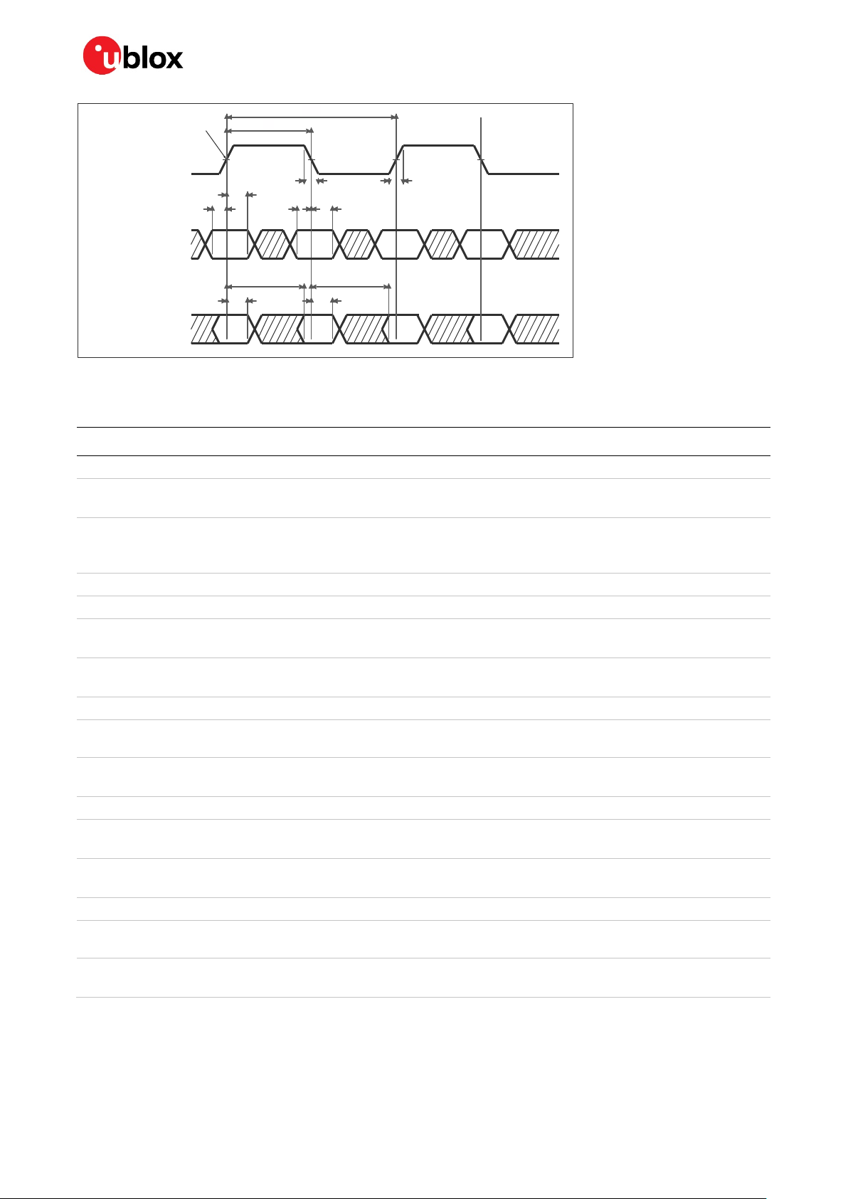
2.4.1 PCM Interface specifications
Figure 9: PCM timing specification – Master mode
Symbol Parameter Condition Min. Typ Max. Units
FBCLK PCM clock frequency - - 2/2.048 - MHz
Duty Cycle
T
BCLK rise/fall
TDO - - - - 15 ns
T
- - 20 - - ns
DISU
T
- - 15 - - ns
DIHO
TBF - - - - 15 ns
Table 13: PCM timing specification – Master mode
- 0.4 0.5 0.6 -
BCLK
- - - 3 - ns
UBX-18017567 - R07 Interfaces Page 15 of 39
C1 - Public
Page 16
JODY-W2 series - Data sheet
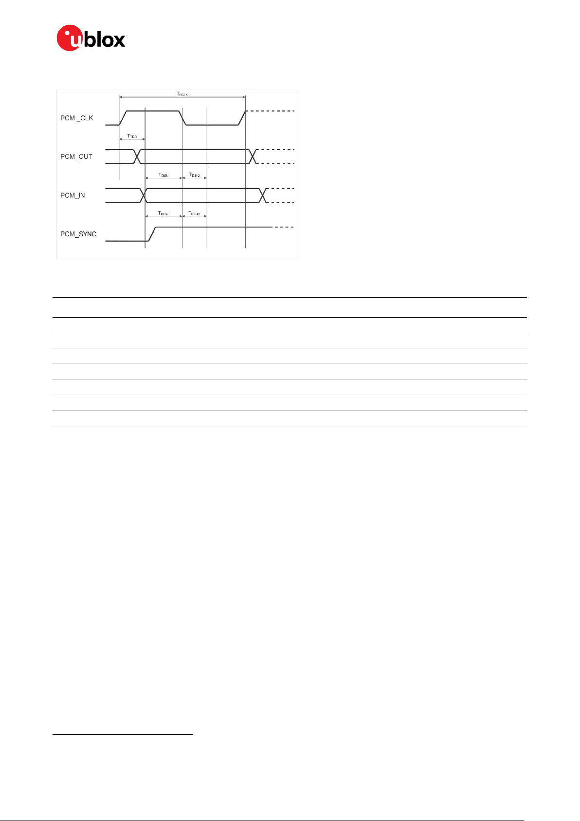
Figure 10: PCM timing specification – Slave mode
Symbol Parameter Condition Min. Typ Max. Units
FBCLK PCM clock frequency - - 2/2.048 - MHz
Duty Cycle
T
BCLK rise/fall
TDO - - - - 30 ns
T
- - 20 - - ns
DISU
T
- - 15 - - ns
DIHO
TBF - - - - 15 ns
Table 14: PCM timing specification – Slave mode
- 0.4 0.5 0.6 -
BCLK
- - - 3 - ns
2.5 LTE Coexistence interface
To manage wireless medium sharing for optimal coexistence performance2, an external handshake
through the LTE Coexistence interface enables signaling between the JODY-W2 series modules and
an external co-located wireless device.
2
LTE coexistence interface is not supported in current firmware.
UBX-18017567 - R07 Interfaces Page 16 of 39
C1 - Public
Page 17
JODY-W2 series - Data sheet
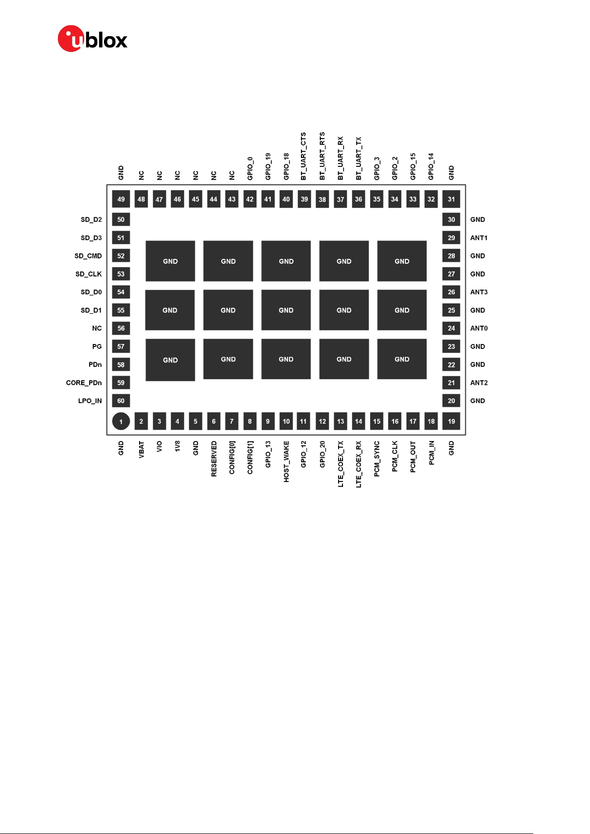
3 Pin definition
3.1 Pin description
Figure 11: JODY-W2 pin assignment (top view)
UBX-18017567 - R07 Pin definition Page 17 of 39
C1 - Public
Page 18

JODY-W2 series - Data sheet
, Output if
, Output if
Function Pin Name Pin No. Power Type Signal Name Remarks
Power VBAT 2 VBAT PWR Module supply input Voltage supply range:
2.8 V – 5.5 V
VIO 3 VIO PWR VIO supply Nominal supply range:
1.8 V or 3.3 V
1V8 4 1V8 PWR VIO supply for SDIO
Supply for analog part
GND 1, 5, 19, 20, 22,
23, 25, 27, 28,
30, 31, 49
Exposed Pins - GND GND Connect to Ground
SDIO host
interface
UART host
interface
PCM
interface
Configuration CONFIG[0] 7 1V8 I Configuration pin See section 2.1 for
Clock and
power
up/down
interface
SD_CLK 53 1V8 I SDIO Clock SDIO Clock input
SD_CMD 52 1V8 I/O SDIO Command SDIO command line
SD_D0 54 1V8 I/O SDIO data 0 SDIO data line bit [0]
SD_D1 55 1V8 I/O SDIO data 1 SDIO data line bit [1]
SD_D2 50 1V8 I/O SDIO data 2 SDIO data line bit [2]
SD_D3 51 1V8 I/O SDIO data 3 SDIO data line bit [3]
BT_UART_TX 36 VIO O UART TX Bluetooth UART,
BT_UART_RX 37 VIO I UART RX Bluetooth UART,
BT_UART_RTS 38 VIO O UART RTS Bluetooth UART,
BT_UART_CTS 39 VIO I UART CTS Bluetooth UART,
PCM_CLK 16 VIO I/O PCM clock Input if slave
PCM_SYNC 15 VIO I/O PCM Frame Sync Input if slave
PCM_IN 18 VIO I PCM data in
PCM_OUT 17 VIO O PCM data out
CONFIG[1] 8 1V8 I Configuration pin See section 2.1 for
RESERVED
CONFIG[2]
PDn 58 1V8 PDn Wi-Fi power enable Power-down interface
CORE_PDn 59 1V8 I CORE_PDn Enable pin of the core
6 1V8 Reserved for future
GND GND
Nominal supply: 1.8 V
connect to Host RX
connect to Host TX
connect to Host CTS
connect to Host RTS
master
master
bootstrap
configuration
bootstrap
configuration
configuration,
A “DNI” pull-up
resistor should be
added at this pin to
respond to future
chipset changes.
of the chipset:
0 = power-down mode
1 = normal mode
voltage regulator.
0 = power supply off
Connect with PDn
UBX-18017567 - R07 Pin definition Page 18 of 39
C1 - Public
Page 19

JODY-W2 series - Data sheet
Function Pin Name Pin No. Power Type Signal Name Remarks
LPO_IN 60 - I Sleep clock input 32.768 kHz clock
input.
Only supported on
professional grade
variant, JODY-W26300B
PG 57 - OD Open-drain output
from the internal
DC/DC converter,
which indicates the
power quality of the
2.2 V rail. High
impedance indicates
power good. Low level
indicates 2.2V is not in
power good.
A (100kΩ) pull-up
resistor must be
connected to this pin
to detect the power
good state.
GPIOs LTE_COEX_TX 13 VIO O UART TX Not supported in
current firmware
LTE_COEX_RX 14 VIO I UART RX Not supported in
current firmware
HOST_WAKE 10 VIO O Host wake-up signal
output
GPIO_0 42 VIO I/O GPIO
GPIO_2 34 VIO I/O GPIO
GPIO_3 35 VIO I/O GPIO
GPIO_12 11 VIO I/O GPIO
GPIO_13 9 VIO I GPIO
GPIO_14 32 VIO I/O GPIO
GPIO_15 33 VIO I/O GPIO
GPIO_18 40 VIO I/O GPIO
GPIO_19 41 VIO I/O GPIO
GPIO_20 12 VIO I/O GPIO
Radio ANT0 24 VBAT RF Antenna signal Bluetooth
ANT1 29 VBAT RF Antenna signal Wi-Fi Dual Band
ANT2 21 - - Not used Do not connect
ANT3 26 - - Not used Do not connect
Other NC 21, 26, 43, 44,
45, 46, 47 48, 56
- - Reserved Do not connect
Asserted: Host device
must wake-up or
remain awake
De-asserted: Host
device can sleep when
the sleep criteria is
met
Table 15: JODY-W2 series pin description
UBX-18017567 - R07 Pin definition Page 19 of 39
C1 - Public
Page 20

JODY-W2 series - Data sheet
4 Electrical specification
⚠ Operating JODY-W2 modules above any of the absolute maximum ratings shown in Table 16 can
cause permanent damage to the device. Extended exposure to conditions outside of the absolute
maximum ratings can also affect the device reliability.
4.1 Absolute maximum ratings
Symbol Description Min. Max. Units
VBAT Power supply voltage -0.3 7.0 V
VIO I/O supply voltage 1.8V/3.3V - 4.0 V
1V8 Analog power supply voltage 1.8V - 1.98 V
T
Storage temperature -40 +1053 ºC
STORAGE
Table 16: Absolute maximum ratings
⚠ The product is not protected against overvoltage or reversed voltages. Voltage spikes exceeding
the power supply voltage specification, given in table above, must be limited to values within the
specified boundaries by using appropriate protection devices.
4.2 Operating conditions
Symbol Parameter Min. Typ Max. Units
VBAT Power supply voltage 2.8 - 5.5 V
VIO I/O supply voltage 1.8V 1.67 - 1.92 V
I/O supply voltage 3.3V 3.07 - 3.53 V
1V8 Analog power supply voltage 1.8V 1.71 1.8 1.89 V
TA Ambient operating temperature
JODY-W263-00A/B
Ambient operating temperature
JODY-W263-01A
Ripple Noise Peak-to-peak voltage ripple on all supply lines. - - 10 mV
Table 17: Operating conditions
☞ Operating condition ranges specified in Table 17 define the limits within which the
functionality of the device is guaranteed.
-40 - +85 ºC
-40 - +105 ºC
3
Qualification pending
UBX-18017567 - R07 Electrical specification Page 20 of 39
C1 - Public
Page 21

JODY-W2 series - Data sheet
4.3 Wi-Fi power consumption
Peak current condition Temperature VBAT (3.3 V) [A] 1V8 (1.8 V) [A]
Active transmission Room temperature 0.5 0.18
T_max (105° C) 0.8 0.2
Firmware Initialization Room temperature 0.7 0.2
T_max (105° C) 0.7 0.2
Table 18: Peak current consumption
Wi-Fi operation modes
Power – save modes
Power down 5.97 0.04 7
Wi-Fi and BT both in deep-sleep4 7.74 0.85 66
IEEE Power Save DTIM 1 and BT deep-sleep 8.71 1.60 63
IEEE Power Save DTIM 2 and BT deep-sleep 8.26 1.26 64
IEEE Power Save DTIM 3 and BT deep-sleep 8.04 1.08 63
Active transmit modes
CCK 11 Mbps, BW20, Ch7, Core2, 18 dBm 355 75 60
MSC7, HT20, Ch7, Core2, 15dBm 265 70 60
BPSK, 6 Mbps, HT20, Ch100, 18 dBm 320 131 60
MCS7, HT20, CH100, 15 dBm 250 120 60
MCS9, VHT40, Ch100, 15 dBm 273 126 60
MCS9, VHT80, Ch100, 15 dBm 300 130 60
Table 19: Wi-Fi radio typical current consumption with different modes of operation
VBAT (3.3 V) [mA] 1V8 (1.8 V) [mA]
VIO (1.8 V) [µA]
4
The high sleep current of 7.74mA is seen in deep-sleep mode because of the DC-DC converter used in the module which has a
quiescent current of 5.7mA. A new design is under development with an alternate DC-DC converter with very low quiescent
current.
UBX-18017567 - R07 Electrical specification Page 21 of 39
C1 - Public
Page 22

JODY-W2 series - Data sheet
4.4 Bluetooth power consumption
Bluetooth operation modes VBAT (3.3 V) [mA] 1V8 (1.8 V) [mA] VIO (1.8 V) [µA]
Operating modes
BLE advertisement 8.21 1.45 64
BT page scan 7.83 0.98 64
BT page & inquiry scan 7.89 1.13 64
Active transmit/receive mode (average over 100ms, measured using HCI commands)
BT TX, pattern - DH5, power: 4 dBm, Ch1 13.62 2.00 64
BT TX, pattern - DH5, power: 10 dBm, Ch1 14.34 6.87 64
BT RX pattern - DH5, Ch1 14.08 5.05 64
BLE TX 14.86 8.77 64
BLE RX 17.40 15.71 64
Table 20: Bluetooth radio typical current consumption with different operating modes
4.5 Digital pad ratings
Symbol Parameter VIO Min. Max. Units
VIH Input high voltage 1.8 V - 3.3 V 0.7*VIO VIO+0.4 V
VIL Input low voltage 1.8 V - 3.3 V -0.4 0.3*VIO V
V
HYS
VOH Output high voltage 1.8 V - 3.3V VIO-0.4 - V
VOH Output low voltage 1.8 V - 3.3 V - 0.4 V
Table 21: DC characteristics VIO
Input hysteresis 1.8 V - 3.3 V 100 - mV
4.6 Radio specifications
4.6.1 Bluetooth
Parameter Specification
RF Frequency Range 2.4 – 2.5 GHz
Supported Modes Bluetooth 5
Number of channels 79 (BR/EDR)
40 (LE)
1 Mbps: GFSK (BR)
Modulation
Transmit Power
Receiver sensitivity
(typical values)
2 Mbps: π/4 DQPSK (EDR)
3 Mbps: 8DQPSK (EDR)
Class 1 BR +10 dBm
Class 1 EDR +9 dBm
LE +8 dBm
BR -87 dBm ± 1.5 dB
EDR -86 dBm ± 1.5 dB
LE -99 dBm ± 1.5 dB
Table 22: Bluetooth radio parameters
UBX-18017567 - R07 Electrical specification Page 22 of 39
C1 - Public
Page 23

JODY-W2 series - Data sheet
802.11a/g/n/ac
OFDM
802.11b
1, 2, 5.5, 11 Mbps
(typ. output power tolerance ± 2 dB)
OFDM, BPSK
-8 dB
19 dBm
OFDM, 64-QAM, 3/4
-25 dB
15 dBm
OFDM, 64-QAM, 5/6
-28 dB
15 dBm
OFDM, 256-QAM, 3/4
-30 dB
15 dBm
Band
Operating mode
Data rate
Bandwidth
Specification
4.6.2 Wi-Fi
JODY-W2 series modules support dual-band Wi-Fi with 802.11a/b/g/n/ac operation in the 2.4 GHz
and 5 GHz radio bands.
Parameter Operation mode Specification
RF Frequency range
Modulation
802.11b/g/n 2.400 – 2.500 GHz
802.11a/n/ac 4.900 – 5.925 GHz
802.11b CCK and DSSS
Supported data rates
Supported channel bandwidth
Supported guard interval (GI)
Table 23: Wi-Fi radio features and specifications
802.11a/g 6, 9, 12, 18, 24, 36, 48, 54 Mbps
802.11n SISO MCS0 - MCS7 (150 Mbps)
802.11ac SISO MCS0 – MCS9 (433 Mbps)
802.11n 20, 40 MHz
802.11ac 20, 40, 80 MHz
802.11n 400, 800 ns
802.11ac Short guard interval supported
Parameter Frequency Operation mode 802.11 EVM limit Preliminary specification
Maximum
transmit
power
2.4 GHz DSSS/CCK -9 dB 19 dBm5
OFDM, QPSK -13 dB 18 dBm
OFDM, 16-QAM -19 dB 18 dBm
OFDM, 64-QAM, 3/4 -25 dB 17 dBm
OFDM, 64-QAM, 5/6 -28 dB 17 dBm
5 GHz OFDM, BPSK -5 dB 16 dBm
OFDM, QPSK -13 dB 15 dBm
OFDM, 16-QAM -19 dB 15 dBm
Table 24: Wi-Fi Radio maximum transmit power parameter
2.4 GHz 802.11b 1Mbps/2Mbps 20MHz -97dBm/-94dBm
802.11g 6Mbps/9Mbps -89dBm/-88dBm
802.11n MCS0/MCS1 -89dBm/-88dBm
5
FCC output power limit 12 dBm
UBX-18017567 - R07 Electrical specification Page 23 of 39
C1 - Public
OFDM, 256-QAM, 5/6 -32 dB 14 dBm
5.5Mbps/11Mbps -92dBm/-88dBm
12Mbps/18Mbps -86dBm/-84dBm
24Mbps/36Mbps -81dBm/-79dBm
48Mbps/54Mbps -75dBm/-73dBm
Page 24

JODY-W2 series - Data sheet
Band
Operating mode
Data rate
Bandwidth
Specification
24Mbps/36Mbps
-83dBm/-80dBm
48Mbps/54Mbps
-75dBm/-74dBm
MCS0/MCS1
-88dBm/-87dBm
MCS8/MCS9
-67dBm/-65dBm
MCS0/MCS1
-81dBm/-81dBm
MCS2/MCS3
-79dBm/-76dBm
MCS2/MCS3 -86dBm/-84dBm
MCS4/MCS5 -81dBm/-79dBm
MCS6/MCS7 -75dBm/-73dBm
5 GHz 802.11a 6Mbps/9Mbps 20MHz -88dBm/-87dBm
12Mbps/18Mbps -88dBm/-86dBm
802.11ac
Table 25: Wi-Fi radio sensitivity
20MHz
MCS2/MCS3 -85dBm/-82dBm
MCS4/MCS5 -80dBm/-76dBm
MCS6/MCS7 -75dBm/-73dBm
MCS8 -69dBm
MCS0/MCS1 40MHz -85dBm/-84dBm
MCS2/MCS3 -82dBm/-79dBm
MCS4/MCS5 -77dBm/-73dBm
MCS6/MCS7 -72dBm/-71dBm
80MHz
MCS4/MCS5 -74dBm/-70dBm
MCS6/MCS7 -69dBm/-68dBm
MCS8/MCS9 -63dBm/-61dBm
UBX-18017567 - R07 Electrical specification Page 24 of 39
C1 - Public
Page 25

JODY-W2 series - Data sheet
5 Host drivers and firmware
5.1 General principle
JODY-W2 series modules do not contain any persistent software. A firmware binary is downloaded by
the host operating system driver at start-up.
5.2 Supported operating systems
5.2.1 Linux
The reference driver, developed by NXP and distributed by u-blox, is only made available to customers
that have signed a limited use license agreement (LULA) [4] with u-blox. A valid non-disclosure
agreement (NDA) is mandatory to get the driver package directly from NXP. The package includes:
• Dedicated kernel driver that binds the Wi-Fi device to the kernel. Driver sources are provided.
• Dedicated Wi-Fi firmware image that is uploaded during initialization of the Wi-Fi device.
• Dedicated Bluetooth firmware image that is uploaded during initialization of the Bluetooth device.
• Laboratory and manufacturing tools.
5.2.2 Android
The Linux driver can be integrated with Android BSP. Detailed instructions for integrating the
operating system on the module are provided in the application note [5].
UBX-18017567 - R07 Host drivers and firmware Page 25 of 39
C1 - Public
Page 26

JODY-W2 series - Data sheet
D
E
F
HDD
GGE
D
A
I
B
F
F
L
K
M
J
Seating
ccc
Plane
C
H
Pin1
P
P
Keep this area free of copper*
Keep this area free of copper*
N
O
J
O
R
R
Future module variants can have more pins in this
area. To en sure compat ibility thi s area shoul d be kept
free of copper.
*
6 Mechanical specifications
Figure 12: JODY-W2 series dimensions (bottom view)
Parameter Description Typical Tolerance
A Module length [mm] 19.8 (779.5 mil) +0.35/-0.1 (+13.8/-3.9 mil)
B Module width [mm] 13.8 (543.3 mil) +0.1/-0.1 (+3.9/-3.9 mil)
C Module thickness [mm] 2.5 (98.4 mil) +0.2/-0.2 (+7.9/-7.9 mil)
ccc Seating plane coplanarity [mm] <0.1 (3.94 mil)
D PCB edge-to-pin Edge [mm] 0.3 (11.8 mil) +0.20/-0.20 (+7.9/-7.9 mil)
E Pin width [mm] 0.7 (27.6 mil) +0.05/-0.05 (+2.0/-2.0 mil)
F Pin length [mm] 0.95 (37.4 mil) +0.05/-0.05 (+2.0/-2.0 mil)
G Pin to pin pitch [mm] 1.0 (39.4 mil) +0.02/-0.02 (+0.8/-0.8 mil)
H Horizontal corner pin-to-pin pitch [mm] 1.125 (44.3 mil) +0.02/-0.02 (+0.8/-0.8 mil)
I Lateral corner pin-to-pin pitch [mm] 1.125 (44.3 mil) +0.02/-0.02 (+0.8/-0.8 mil)
J Horizontal thermal pads pitch [mm] 3.2 (126.0 mil) +0.02/-0.02 (+0.8/-0.8 mil)
K Thermal pad height [mm] 2.2 (86 6 mil) +0.1/-0.1 (+3.9/-3.9 mil)
L Thermal pad length [mm] 2.7 (106.3 mil) +0.1/-0.1 (+3.9/-3.9 mil)
M Pin 1 diameter [mm] 0.95 (37.4 mil) +0.05/-0.05 (+2.0/-2.0 mil)
N Horizontal pin-to-thermal pad pitch [mm] 3.425 (134.8 mil) +0.02/-0.02 (+0.8/-0.8 mil)
O Lateral pin-to-thermal pad distance [mm] 2.725 (107.3 mil) +0.02/-0.02 (+0.8/-0.8 mil)
P Lateral thermal pads pitch [mm] 2.7 (106.3 mil) +0.02/-0.02 (+0.8/-0.8 mil)
R Reserved area for future module variants 1.55 (61.0 mil) +0.05/-0.05 (+2.0/-2.0 mil)
Table 26: Description of parameters
UBX-18017567 - R07 Mechanical specifications Page 26 of 39
C1 - Public
Page 27

JODY-W2 series - Data sheet
7 Approvals
JODY-W2 series modules comply with the regulatory demands of Radio Equipment Directive (RED),
Federal Communications Commission (FCC), Innovation Science and Economic Development (ISED)
⚠ All approvals are pending.
☞ See JODY-W2 series System Integration Manual [2] for detailed information about regulatory
compliance requirements of end products that use JODY-W2 series modules.
7.1 European Union regulatory compliance
For information about the regulatory compliance of JODY-W2 series modules against requirements
and provisions in the European Union, see JODY-W2 Declaration of Conformity [9].
⚠ All approvals are pending.
7.1.1 Radio Equipment Directive (RED) 2014/53/EU
JODY-W2 series modules comply with the essential requirements and other relevant provisions of
Radio Equipment Directive (RED) 2014/53/EU.
Essential Requirements
Radio Equipment Directive 2014/53/EU
Health and safety
(Article 3.1a)
EMC
(Article 3.1b)
Radio Spectrum Efficiency
(Article 3.2)
Essential Requirements
RoHS Directive 2011/65/EU
Prevention
(Article 4.1)
Standards
EN 62368-1:2014+A11:2017
EN 62311:2008 (Wi-Fi)
EN 62479:2010 (Bluetooth and Bluetooth Low Energy)
EN 301 489-1 V2.1.1
EN 301 489-17 V3.1.1
EN 300 328 V2.2.2
EN 301 893 V2.1.1
EN 300 440 V2.1.1
Standards
EN 50581:2012
6
.
7.1.2 Compliance with the RoHS directive
JODY-W2 series modules comply with the Directive 2011/65/EU (EU RoHS 2) and its amendment
Directive (EU) 2015/863 (EU RoHS 3).
7.2 United States (FCC)
This section contains the FCC compliance information for the JODY-W2 series modules.
⚠ Approvals are pending.
Below is the list of the FCC IDs allocated to JODY-W2 series modules.
6
Approvals are pending.
UBX-18017567 - R07 Approvals Page 27 of 39
C1 - Public
Page 28

JODY-W2 series - Data sheet
Model7 FCC ID
JODY-W263-00A, JODY-W263-01A, JODY-W263-00B XPYJODYW263
Table 27: FCC and ISED IDs for different variants of JODY-W2 series modules
7.2.1 FCC compliance statement
The JODY-W2 series modules have modular approval and comply with Part 15 of the FCC Rules.
Operation is subject to the following two conditions:
1. This device may not cause harmful interference, and
2. This device must accept any interference received, including interference that may cause
undesired operation.
⚠ Any changes or modifications NOT explicitly APPROVED by u-blox could cause the JODY-W2
series module to cease to comply with FCC rules part 15 thus void the user's authority to operate
the equipment.
The internal / external antenna(s) used for this module must provide a separation distance of at least
20 cm from all persons and must not be co-located or operating in conjunction with any other antenna
or transmitter.
In accordance with 47 CFR § 15.19, the end product into which this module is integrated shall bear
the following statement in a conspicuous location on the device:
“This device complies with Part 15 of the FCC Rules. Operation is subject to the following two
conditions:
1. This device may not cause harmful interference, and
2. This device must accept any interference received, including interference that may cause
undesired operation.”
When the end-product is so small or for such use that it is not practical to place the above statement
on it, the information shall be placed in a prominent location in the instruction manual or pamphlet
supplied to the user or on the container in which the device is marketed. However, the FCC ID label
must be displayed on the device.
If the end-product will be installed in locations where the end-user is not able to see the FCC ID and/or
this statement, the FCC ID and the statement shall also be included in the end-product manual.
☞ The outside of final products containing the JODY-W2 module must display in a user accessible
area a label referring to the enclosed module. This exterior label can use wording such as the
following: “Contains Transmitter Module FCC ID: XPYJODYW263” or “Contains FCC ID:
XPYJODYW263”.
7.3 Canada (ISED)
⚠ Approvals are pending.
JODY-W2 series module are certified for use in accordance with the Canada Innovation, Science and
Economic Development Canada (ISED) Radio Standards Specification (RSS) RSS-247 Issue 2 and
RSSGen. Below is the list of the ISED IDs allocated to JODY-W2 series modules.
Model ISED certification number
JODY-W263-00A, JODY-W263-01A, JODY-W263-00B 8595A-JODYW263
Table 28: ISED ID for different variants of JODY-W2 series modules
7
The model name is identical to the ordering code. Refer to Table 33 for details.
UBX-18017567 - R07 Approvals Page 28 of 39
C1 - Public
Page 29

JODY-W2 series - Data sheet
7.3.1 ISED compliance statement
The JODY-W2 series module complies with ISED (Innovation, Science and Economic Development
Canada)
(1) This device may not cause interference, and
(2) This device must accept any interference, including interference that may cause undesired
operation of the device.
8
license-exempt RSSs. Operation is subject to the following two conditions:
☞ Any notification to the end user of installation or removal instructions about the integrated radio
module is NOT allowed. Unauthorized modification could void authority to use this equipment.
This equipment complies with ISED RSS-102 radiation exposure limits set forth for an uncontrolled
environment. This equipment should be installed and operated with minimum distance 20 cm
between the radiator and your body.
This radio transmitter IC: 8595A-JODYW263 has been approved by ISED to operate with the antenna
types listed below with the maximum permissible gain indicated. Antenna types not included in this
list, having a gain greater than the maximum gain indicated for that type, are strictly prohibited for
use with this device.
☞ Operation in the band 5150–5250 MHz is only for indoor use to reduce the potential for harmful
interference to co-channel mobile satellite systems;
☞ Operation in the 5600-5650 MHz band is not allowed in Canada. High-power radars are allocated
as primary users (i.e. priority users) of the bands 5250-5350 MHz and 5650-5850 MHz and that
these radars could cause interference and/or damage to LE-LAN devices.
The ISED certification label of a module shall be clearly visible at all times when installed in the host
device; otherwise, the host device must be labeled to display the ISED certification number for the
module, preceded by the words “Contains transmitter module”, or the word “Contains”, or similar
wording expressing the same meaning, as follows: “Contains transmitter module IC: 8595AJODYW263”.
Le présent appareil est conforme aux CNR d'ISED applicables aux appareils radio exempts de licence.
L'exploitation est autorisée aux deux conditions suivantes:
(1) l'appareil ne doit pas produire de brouillage, et
(2) l'utilisateur de l'appareil doit accepter tout brouillage radioélectrique subi, même si le brouillage est
susceptible d'en compromettre le fonctionnement.
Cet équipement est conforme aux limites d'exposition de rayonnement d'ISED RSS-102 déterminées
pour un environnement non contrôlé. Cet équipement devrait être installé et actionné avec la distance
minimum 20 cm entre le radiateur et votre corps.
Cet émetteur radio, IC: 8595A-JODYW263 été approuvé par ISED pour fonctionner avec les types
d’antenne énumérés ci-dessous avec le gain maximum autorisé et l’impédance nécessaire pour
chaque type d’antenne indiqué. Les types d’antenne ne figurant pas dans cette liste et ayant un gain
supérieur au gain maximum indiqué pour ce type-là sont strictement interdits d’utilisation avec cet
appareil.
☞ Le dispositif de fonctionnement dans la bande 5150-5250 MHz est réservé à une utilisation en
intérieur pour réduire le risque d'interférences nuisibles à la co-canal systèmes mobiles par
satellite
☞ Opération dans la bande 5600-5650 MHz n'est pas autorisée au Canada. Haute puissance radars
sont désignés comme utilisateurs principaux (c.-àutilisateurs prioritaires) des bandes 5250-5350
8
Formerly known as IC (Industry Canada).
UBX-18017567 - R07 Approvals Page 29 of 39
C1 - Public
Page 30

JODY-W2 series - Data sheet
MHz et 5650-5850 MHz et que ces radars pourraient causer des interférences et / ou des
dommages à dispositifs LAN-EL.
L’étiquette d’homologation d’ISED d’un module donné doit être posée sur l’appareil hôte à un endroit
bien en vue en tout temps. En l’absence d’étiquette, l’appareil hôte doit porter une étiquette sur
laquelle figure le numéro d’homologation du module d’ISED, précédé des mots « Contient un module
d’émission », ou du mot « Contient », ou d’une formulation similaire allant dans le même sens et qui va
comme suit : « Contient le module d’émission IC: 8595A-JODYW263 ».
This radio transmitter IC: 8595A-JODYW263 has been approved by ISED to operate with the antenna
types listed below with the maximum permissible gain indicated. Antenna types not included in this
list, having a gain greater than the maximum gain indicated for that type, are strictly prohibited for
use with this device.
Le présent émetteur radio IC: 8595A-JODYW263 a été approuvé par ISED pour fonctionner avec les
types d'antenne énumérés ci-dessous et ayant un gain admissible maximal. Les types d'antenne non
inclus dans cette liste, et dont le gain est supérieur au gain maximal indiqué, sont strictement
interdits pour l'exploitation de l'émetteur.
The internal / external antenna(s) used for this module must provide a separation distance of at least
20 cm from all persons and must not be co-located or operating in conjunction with any other antenna
or transmitter.
☞ The approval type for all the JODY-W2 series variants is a single modular approval. Due to ISED
Modular Approval Requirements (Source: RSP-100 Issue 10), any application which includes the
module must be approved by the module manufacturer (u-blox). The application manufacturer
must provide design data for the review procedure.
7.4 Certification in other countries
Additional country certifications can be progressed upon request. For further information, contact
the support team for your area, as listed in the Contact section.
7.5 Approved antennas
7.5.1 Wi-Fi / Bluetooth dual band antennas
For Bluetooth and Wi-Fi operation in the 2.4 GHz band and Wi-Fi operation in the 5 GHz band, the
module has been tested and approved for use with the antennas listed in Table 28.
Manufacturer Part Number Antenna type Peak gain [dBi] Validated
2.4 GHz band 5 GHz band
Linx ANT-DB1-RAF-RPS Dual-band dipole antenna [6] 2.5 4.6 FCC/ISED, ETSI
Table 29: List of approved dual-band antennas
⚠ Important: To be compliant to FCC §15.407(a) the EIRP is not allowed to exceed 125 mW
(21 dBm) at any elevation angle above 30 degrees as measured from the horizon when operated
as an outdoor access point in U-NII-1 band, 5.150-5.250 GHz.
Regulatory Domain
7.5.2 Bluetooth antenna
The following antennas are designated for Bluetooth transmission on JODY-W2:
Manufacturer Part Number Antenna type Peak gain [dBi]
2.4 GHz band
Linx ANT-2.4-CW-RCT-RP Single-band dipole antenna [8] 2.2 FCC/ISED, ETSI
Table 30: List of approved single-band antennas
UBX-18017567 - R07 Approvals Page 30 of 39
C1 - Public
Validated Regulatory
Domain
Page 31

JODY-W2 series - Data sheet
8 Product handling
8.1 Packaging
For efficient production, production lot set-up and tear-down, JODY-W2 series modules are delivered
as hermetically sealed devices on tape and reel. For more information about packaging, see the
u-blox package Information Guide [1].
8.1.1 Reels
JODY-W2 series modules are deliverable in quantities of 500 pieces on a reel. The modules are
shipped on reel Type A, as described in the u-blox package information guide [1].
8.1.2 Tapes
The dimensions of the tapes are shown in Figure 13.
Figure 13: JODY-W2 Tape dimensions
8.2 Shipment, storage, and handling
☞ For more information regarding shipment, storage and handling see the u-blox package
information guide [1].
8.2.1 Moisture sensitivity levels
JODY-W2 series automotive-grade modules are rated at moisture sensitivity level 3. See moisture
sensitive warning label on each shipping bag for detailed information. After opening the dry pack,
modules must be mounted within 168 hours in factory conditions of maximum 30 °C/60%RH or must
be stored at less than 10%RH. Modules require baking if the humidity indicator card shows more than
10% when read at 23±5°C or if the conditions mentioned above are not met. Please refer to J-STD033B standard for bake procedure.
UBX-18017567 - R07 Product handling Page 31 of 39
C1 - Public
Page 32

JODY-W2 series - Data sheet
•
when handling the PCB must always be
•
•
the RF input, do not touch any exposed
be sure to
•
8.2.2 Mounting process and soldering recommendations
Reflow profiles are to be selected according to u-blox recommendations. See JODY-W2 series System
integration manual [2]
for more information.
8.2.3 ESD handling precautions
⚠ JODY-W2 series modules are Electrostatic Sensitive Devices (ESD). Observe precautions for
handling! Failure to observe these precautions can result in severe damage to the Wi-Fi receiver!
Wi-Fi transceivers are Electrostatic Sensitive Devices (ESD) and require special precautions during
handling. To minimize the risk of damage caused by electrostatic charges, be sure to handle the
patch antennas with care. In addition to standard ESD safety practices, the following measures
should be observed when handling the receiver:
Unless there is a galvanic coupling between
the local GND (on the work bench, or similar)
and the PCB GND, the first point of contact
between the local GND and PCB GND.
• Be sure to ground the module before
mounting an antenna patch.
When handling the RF pin, avoid any contact
with charged capacitors. Also be careful
when contacting materials that can develop
charges, like the patch antenna (~10 pF),
coaxial cable (~50-80 pF/m), soldering iron,
and so on.
To prevent electrostatic discharge through
antenna area. If there is any risk that the
exposed antenna area might be touched in a
non-ESD protected work area,
implement proper ESD protection measures
in the application design.
When soldering RF connectors and patch
antennas to the RF pin of the receiver, be
sure to use an ESD safe soldering iron (tip).
UBX-18017567 - R07 Product handling Page 32 of 39
C1 - Public
Page 33

JODY-W2 series - Data sheet
3
1
6
9 Labeling and ordering information
9.1 Product labeling
The labels of JODY-W2 series include important product information as described in this section. The
data matrix code for automotive and professional grade variants of JODY-W2 series includes a serial
number.
Figure 14 illustrates the sample label of the JODY-W2 series and includes: the u-blox logo, product
name (model), type number, FCC and IC certification number and date of unit production encoded
YY/WW (year/week).
2
4
Figure 14: JODY-W2 series sample label
Detailed descriptions of the label components are shown in Table 30.
Reference Description
1 Text in bold font: MODEL: type number with the product version. Same as product name.
2 Minor product version
3 Date of production encoded YY/WW (year/week)
4 FCC/ISED ID with which the module has been listed with
5 Data Matrix with unique serial number comprising 19 alphanumeric symbols.
The first 3 symbols represent the unique module type number. The following 12 symbols represent the
unique hexadecimal Bluetooth MAC address of the module in the format AABBCCDDEEFF. The last 4
symbols represent the hardware and firmware version encoded HHFF.
6 u-blox logo. The red dot above the logo represents the physical location of pin 1.
5
Table 31: JODY-W2 series label descriptions
UBX-18017567 - R07 Labeling and ordering information Page 33 of 39
C1 - Public
Page 34

JODY-W2 series - Data sheet
9.2 Explanation of codes
Two different product code formats are used. The Product name is used to identify the module in all
related documentation. An appropriate name is given for all u-blox products – regardless of the
packaging and quality grade.
The Ordering code includes options and quality, while the Type Number includes the hardware and
firmware versions. Table 31 describes these three different code formats.
Format Structure
Product name PPPP-TGVV
Ordering code PPPP-TGVV-TTQ
Type number PPPP-TGVV-TTQ-XX
Table 32: Product code formats
Table 32 describes the identification codes associated with each module variant.
Code Description Example
PPPP Form factor JODY
TG Platform
T – Dominant technology, For example, W: Wi-Fi, B: Bluetooth
G - Generation
VV Variant based on the same platform; range [00…99] 63
TT Major Product Version 00
Q Quality grade
A: Automotive
B: Professional
C: Standard
XX Minor product version (not relevant for certification) 00
W2
A
Table 33: Part identification codes
9.3 Ordering codes
Ordering code Product name Product
Automotive grade module based on NXP 88W8987(A) transceiver. Equipped
JODY-W263-00A JODY-W263-A
JODY-W263-01A JODY-W263-A
JODY-W263-00B JODY-W263
Table 34: Product ordering codes
☞ Product changes affecting the form, fit or function of the module are documented by u-blox.
For a list of Product Change Notifications (PCNs) visit www.u-blox.com.
with a single Wi-Fi antenna and one Bluetooth antenna, the module has an
operational temperature of -40
Automotive grade module based on NXP 88W8987S transceiver. Equipped
with a single Wi-Fi antenna and single Bluetooth antenna, the module has an
operational temperature of -40
Professional grade module based on NXP 88W8987(I) transceiver. Equipped
with a single Wi-Fi antenna and single Bluetooth antenna, the module has an
operational temperature of -40
0
C to +85 0C.
0
C to +105 0C.
0
C to +85 0C.
UBX-18017567 - R07 Labeling and ordering information Page 34 of 39
C1 - Public
Page 35

Appendix
A Glossary
Abbreviation Definition
AC Alternating Current
CMD Command
DC Direct Current
DDR Double Data Rate
ESD Electrostatic Sensitive Devices
FCC Federal Communications Commission
FIFO First In, First Out
GI Guard interval
GND Ground
GPIO General-purpose input/output
HD High Definition
HCI Host Controller Interface
ISED Innovation, Science and Economic Development Canada
ISM Industrial, scientific and medical
LE Bluetooth Low Energy
LTE Long Term Evolution
LULA Limited Use License Agreement
MAC Medium Access Control
MIMO Multiple Input Multiple Output
MWS Mobile Wireless Standards
MSL Moisture sensitivity level
NFC Near-Field Communication
OEM Original equipment manufacturer
P2P Peer-to-peer
P2P (GC) P2P Client
P2P (GO) P2P Group Owner
PCB Printed Circuit Board
PCI Peripheral Component Interconnect
PCIe PCI Express
PCN Product Change Notification
PCM Pulse-code modulation
POR Power-on reset
RED Radio Equipment Directive
RF Radio Frequency
RSDB Real Simultaneous Dual Band
RSS Radio Standards Specification
RH Relative humidity
RoHS Restriction of Hazardous Substances
UBX-18017567 - R07 Appendix Page 35 of 39
C1 - Public
Page 36

Abbreviation Definition
SAR Specific Absorption Rate
SCO Synchronous Connection-Oriented
SDIO Secure Digital Input Output
SDR Single Data Rate
SISO Single-input single-output
SMD Surface-mount Device
STA Station
TBD To be defined
USB Universal Serial Bus
UART Universal Asynchronous Receiver/Transmitter
VSDB Virtual Simultaneous Dual Band
WAPI WLAN Authentication and Privacy Infrastructure
WLAN Wireless Local Area Network
Table 35: Explanation of the abbreviations and terms used
UBX-18017567 - R07 Appendix Page 36 of 39
C1 - Public
Page 37

Related documents
[1] u-blox package information guide, UBX-14001652
[2] JODY-W2 series, system integration manual, UBX-18068879
[3] Radio Equipment Directive (RED);
https://ec.europa.eu/growth/sectors/electrical-engineering/red-directive; July 2017a
[4] u-blox Limited Use License Agreement (LULA-M)
[5] Android integration, application note, UBX-19035432
[6] ANT-DB1-RAF-XXX Data sheet, Linx, https://linxtechnologies.com/wp/wp-
content/uploads/ant-db1-raf-fff.pdf
[7] GW.40.2153 Data sheet, Taoglas, https://fccid.io/pdf.php?id=2415249
[8] ANT-2.4-CW-RCT-XX Data Sheet, Linx, https://linxtechnologies.com/wp/wp-
content/uploads/ant-2.4-cw-rct-cc.pdf
[9] JODY-W2 Declaration of Conformity, UBX-20053576
☞ For product change notifications and regular updates of u-blox documentation, register on our
website, www.u-blox.com.
UBX-18017567 - R07 Related documents Page 37 of 39
C1 - Public
Page 38

and
going
pdate of this data sheet will
Revision history
Revision Date Name Comments
R01 20-Nov-2018 shoe, mhei,
kgom
R02 09-Apr-2019 vbak Updated (Pin name “BT_DEV_WAKE”). Changed the power domain for SDIO
R03 02-May-2019 kgom Changed product status for JODY-W263-01A-00 to Prototype.
R04 25-Apr-2020 vbak, aheg Corrected pin 59 description and Wi-Fi/Bluetooth output power (Table 21
R05 7-Dec-2020 lber, aheg Updated the regulatory compliance section with the details about on-
R06 11-Dec-2020 mzes Corrected product name and chipset references in document information and
R07 28-Jan-2021 vbak Corrected Wi-Fi simultaneous operation modes in section 1.4.2.
Initial release.
lines (Table 15).
Table 22). Added current consumption values (section ☞). Updated pin list.
Updated the mechanical specifications (Figure 12).
certifications. Approvals are pending. A further u
be distributed once certification reports are available.
section 1.4.
UBX-18017567 - R07 Revision history Page 38 of 39
C1 - Public
Page 39

Support: support_tw@u-blox.com
Contact
For complete contact information, visit us at www.u-blox.com.
u-blox Offices
North, Central and South America
u-blox America, Inc.
Phone: +1 703 483 3180
E-mail: info_us@u-blox.com
Regional Office West Coast:
Phone: +1 408 573 3640
E-mail: info_us@u-blox.com
Technical Support:
Phone: +1 703 483 3185
E-mail: support@u-blox.com
Headquarters
Europe, Middle East, Africa
u-blox AG
Phone: +41 44 722 74 44
E-mail: info@u-blox.com
Support: support@u-blox.com
Asia, Australia, Pacific
u-blox Singapore Pte. Ltd.
Phone: +65 6734 3811
E-mail: info_ap@u-blox.com
Support: support_ap@u-blox.com
Regional Office Australia:
Phone: +61 2 8448 2016
E-mail: info_anz@u-blox.com
Support: support_ap@u-blox.com
Regional Office China (Beijing):
Phone: +86 10 68 133 545
E-mail: info_cn@u-blox.com
Support: support_cn@u-blox.com
Regional Office China (Chongqing):
Phone: +86 23 6815 1588
E-mail: info_cn@u-blox.com
Support: support_cn@u-blox.com
Regional Office China (Shanghai):
Phone: +86 21 6090 4832
E-mail: info_cn@u-blox.com
Support: support_cn@u-blox.com
Regional Office China (Shenzhen):
Phone: +86 755 8627 1083
E-mail: info_cn@u-blox.com
Support: support_cn@u-blox.com
Regional Office India:
Phone: +91 80 405 092 00
E-mail: info_in@u-blox.com
Support: support_in@u-blox.com
Regional Office Japan (Osaka):
Phone: +81 6 6941 3660
E-mail:
Support: support_jp@u-blox.com
Regional Office Japan (Tokyo):
Phone: +81 3 5775 3850
E-mail: info_jp@u-blox.com
Support: support_jp@u-blox.com
Regional Office Korea:
Phone: +82 2 542 0861
E-mail: info_kr@u-blox.com
Support: support_kr@u-blox.com
Regional Office Taiwan:
Phone: +886 2 2657 1090
E-mail: info_tw@u-blox.com
info_jp@u-blox.com
UBX-18017567 - R07 Contact Page 39 of 39
C1 - Public
 Loading...