

Page 1

EVK-NINA-W1/EVK-NINA-B2
Evaluation kit for NINA-W1 and NINA-B2 modules
User guide
Abstract
This document describes how to set up the EVK-NINA-W1/EVK-NINA-B2 evaluation kits to evaluate
NINA-W1 series and NINA-B2 series stand-alone modules. It also describes the different options for
debugging and the development capabilities included in the evaluation board.
UBX-17011007 - R09 C1-Public www.u-blox.com
Page 2

EVK-NINA-W1/EVK-NINA-B2 - User guide
u-blox or third parties may hold intellectual property rights in the products, names, logos and designs included in this
document. Copying, reproduction, modification or disclosure to third parties of this document or any part thereof is only
permitted wit
The information contained herein is provided “as is” and u
implied, is given, including but not limited
purpose of the information. This document may be revised by u
documents, visit www.u
Copyright © u
Document information
Title EVK-NINA-W1/EVK-NINA-B2
Subtitle Evaluation kit for NINA-W1 and NINA-B2 modules
Document type User guide
Document number UBX-17011007
Revision and date R09 2-Feb-2021
Disclosure restriction
C1-Public
This document applies to the following products:
Product name Software version
EVK-NINA-B221 All
EVK-NINA-B222 All
EVK-NINA-W101 N/A
EVK-NINA-W102 N/A
EVK-NINA-W106 N/A
EVK-NINA-W131 All
EVK-NINA-W132 All
EVK-NINA-W151 All
EVK-NINA-W152 All
EVK-NINA-W156 All
UBX-17011007 - R09 Document information Page 2 of 29
C1-Public
h the express written permission of u-blox.
-blox assumes no liability for its use. No warranty, either express or
to, with respect to the accuracy, correctness, reliability and fitness for a particular
-blox at any time without notice. For the most recent
-blox.com.
-blox AG.
Page 3

EVK-NINA-W1/EVK-NINA-B2 - User guide
Contents
Document information ............................................................................................................................. 2
1 Product description ............................................................................................................................ 4
1.1 Overview ........................................................................................................................................................ 4
1.2 Kit includes ................................................................................................................................................... 6
1.2.1 EVK-NINA-B221 and EVK-NINA-W1x1 .......................................................................................... 6
1.2.2 EVK-NINA-B222 and EVK-NINA-W1x2 .......................................................................................... 6
1.2.3 EVK-NINA-W1x6 ................................................................................................................................. 6
1.3 I/O allocation................................................................................................................................................. 7
1.4 Jumper description .................................................................................................................................... 8
1.4.1 Default jumper configuration ......................................................................................................... 10
1.5 LEDs ............................................................................................................................................................. 10
1.5.1 RGB-LED jumper configuration ..................................................................................................... 11
1.6 Connectors ................................................................................................................................................. 12
1.7 Buttons ........................................................................................................................................................ 12
1.8 Configuration options .............................................................................................................................. 13
1.8.1 UART ................................................................................................................................................... 13
1.8.2 Power supply ...................................................................................................................................... 13
1.8.3 Low-power Oscillator (LPO) ............................................................................................................ 14
1.8.4 RMII to PHY ........................................................................................................................................ 14
1.8.5 SPI slave interface ............................................................................................................................ 14
2 Setting up the evaluation board .................................................................................................. 16
2.1 EVK without software (open CPU) ......................................................................................................... 16
2.2 EVK with u-blox connectivity software ................................................................................................. 17
2.2.1 Starting up ......................................................................................................................................... 17
2.2.2 Getting the latest software ............................................................................................................ 17
Appendix .................................................................................................................................................... 18
A Layout EVK-NINA-W1x1, -W1x2 and EVK-NINA-B221, -B222 .......................................... 18
B Layout EVK-NINA-W1x6 ................................................................................................................ 18
C Schematic drawing EVK-NINA-W1x1, -W1x2 and EVK-NINA-B221, -B222 ................... 19
D Schematic drawing EVK-NINA-W1x6 ........................................................................................ 23
E Glossary .............................................................................................................................................. 27
Related documents ................................................................................................................................ 28
Revision history ....................................................................................................................................... 28
Contact ....................................................................................................................................................... 29
UBX-17011007 - R09 Document information Page 3 of 29
C1-Public
Page 4

EVK-NINA-W1/EVK-NINA-B2 - User guide
1 Product description
1.1 Overview
The EVK-NINA-W1/EVK-NINA-B2 evaluation kit includes an evaluation board, which can be used as a
reference design for the NINA-W1 or NINA-B2 series modules, a quick start guide, and a USB cable.
For the NINA-B221 and the NINA-W1x1 module, the evaluation board is prepared with a U.FL coaxial
connector for connecting the external antenna. The NINA-B222 and the NINA-W1x2 modules have an
onboard PIFA antenna. The NINA_W1x6 have a PCB trace antenna; thus the EVK-NINA-B222, the
EVK-NINA-W1x2 and EVK-NINA-W1x6 evaluation boards do not have a U.FL connector.
The main features of the EVK-NINA-W1/EVK-NINA-B2 are:
• Available in several variants:
o NINA-B221 and NINA-B222
o NINA-W101 and NINA-W102
o NINA-W131 and NINA-W132
o NINA-W151 and NINA-W152
o NINA-W106 and NINA-W156
• All of the module pins are available at connectors or jumpers
• Can be powered through USB (J8) or external power supply (J23)
• Equipped with a Quad High Speed USB to Multipurpose UART/MPSSE IC (FT4232) that allows
serial communication and flashing over USB.
The EVK-NINA-W1/EVK-NINA-B2 evaluation kits are available in the following variants, depending on
the NINA module that is mounted on the EVK:
• EVK-NINA-B221 – Evaluation kit for NINA-B221 module, RF port available on U.FL connector (J21)
• EVK-NINA-B222 – Evaluation kit for NINA-B222 module with onboard PIFA antenna
• EVK-NINA-W101 – Evaluation kit for NINA-W101 module, RF port available on U.FL connector
(J21)
• EVK-NINA-W102 – Evaluation kit for NINA-W102 module with onboard PIFA antenna
• EVK-NINA-W106 – Evaluation kit for NINA-W106 module with a PCB trace antenna
• EVK-NINA-W131 – Evaluation kit for NINA-W131 module, RF port available on U.FL connector
(J21)
• EVK-NINA-W132 – Evaluation kit for NINA-W132 module with onboard PIFA antenna
• EVK-NINA-W151 – Evaluation kit for NINA-W151 module, RF port available on U.FL connector
(J21)
• EVK-NINA-W152 – Evaluation kit for NINA-W152 module with onboard PIFA antenna
• EVK-NINA-W156 – Evaluation kit for NINA-W156 module with a PCB trace antenna
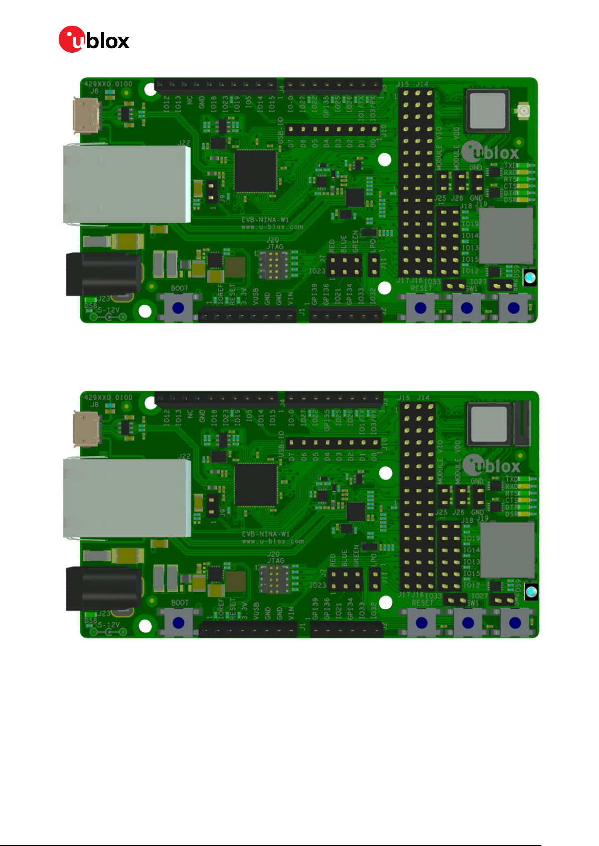
This section describes the main connectors and settings that are required to get started. Figure 1,
Figure 2 and Figure 3 shows the three different antenna variants of the EVK-NINA-W1/EVK-NINA-B2
evaluation board.
UBX-17011007 - R09 Product description Page 4 of 29
C1-Public
Page 5
EVK-NINA-W1/EVK-NINA-B2 - User guide
Figure 1: EVK-NINA-W1x1/ EVK-NINA-B2x1 evaluation board with U.FL connector for external antenna
Figure 2: EVK-NINA-W1x2/ EVK-NINA-B2x2 evaluation board with onboard PIFA antenna
⚠ Take care while handling the EVK-NINA-B222 and EVK-NINA-W1x2. Applying force to the NINA
module might damage the internal PIFA antenna.
UBX-17011007 - R09 Product description Page 5 of 29
C1-Public
Page 6

EVK-NINA-W1/EVK-NINA-B2 - User guide
Figure 3: EVK-NINA-W1x6 evaluation board with internal PCB trace antenna
1.2 Kit includes
1.2.1 EVK-NINA-B221 and EVK-NINA-W1x1
The EVK-NINA-B221 and EVK-NINA-W1x1 evaluation kits include the following:
• EVK-NINA-B221 or EVK-NINA-W1x1 evaluation board
• 2.4 GHz foldable antenna (Ex-It 2400) with reverse polarity SMA connector
• RP-SMA - U.FL cable assembly, 100 mm length
• USB cable
• Thank you card
1.2.2 EVK-NINA-B222 and EVK-NINA-W1x2
EVK-NINA-B222 and EVK-NINA-W1x2 evaluation kits include the following:
• EVK-NINA-B222 and EVK-NINA-W1x2
• USB cable
• Thank you card
1.2.3 EVK-NINA-W1x6
EVK-NINA-W1x6 evaluation kits include the following:
• EVK-NINA-W1x6
• USB cable
• Thank you card
UBX-17011007 - R09 Product description Page 6 of 29
C1-Public
Page 7

EVK-NINA-W1/EVK-NINA-B2 - User guide
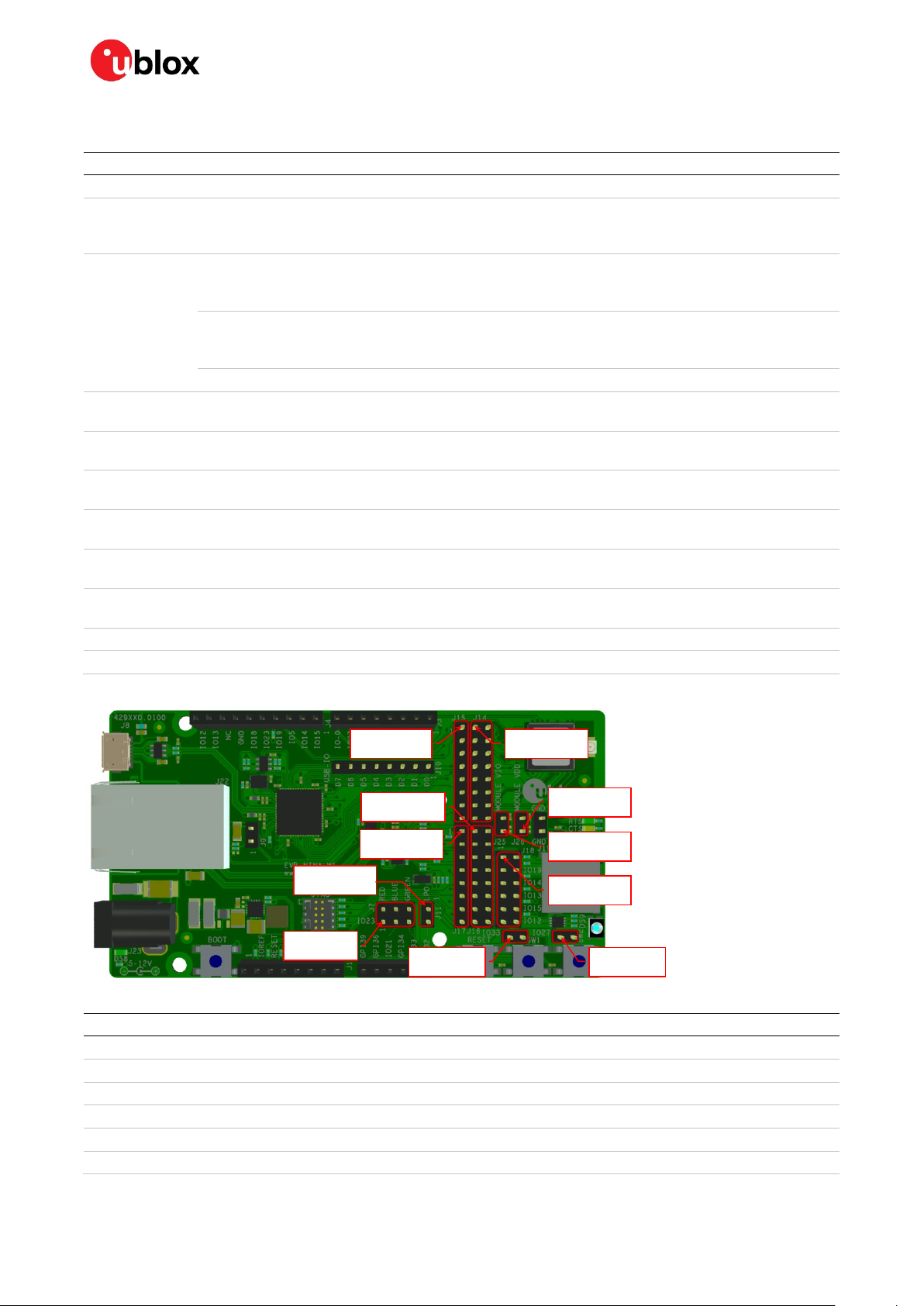
1.3 I/O allocation
The block diagram in Figure 4 provides a better understanding of how I/O signals from the module are
made available at connectors and/or interfaces of the EVK.
Sixteen (16) I/O signals (on EVK-NINA-W1x6 17 signals) are available at the middle row of the I/O
allocator. These signals can be distributed to connectors and/or interfaces on the EVK by use of
jumpers to connect the associated middle and outer row pin(s).
The signals IO-12, IO-13, IO-14 and IO-15 can be disconnected from the J4 connector by not
populating the corresponding jumpers at J18. This can be useful if the SDIO signals D2, D3, CLK, and
CMD are directed to the SD card reader (J19).
Signals on the module not connected to any circuits (interfaces, LEDs and switches etc) on the board
are connected directly to J1, J2, J3 or J4 connector.
* Available only on EVK-NINA-W1x6.
Figure 4: Block diagram of EVK-NINA-W10
☞ When reset-n is released, the module pin 27 (IO-0) is read as boot-n (firmware upgrade). When IO-
0 is connected to the module, it must be high during start up for normal operation.
☞ On EVK-NINA-W1x6 the Micro-SD card is placed on the bottom side. Additionally, the NINA-W1x6
module and the J25/J26 and GND pins have changed places.
UBX-17011007 - R09 Product description Page 7 of 29
C1-Public
Page 8
EVK-NINA-W1/EVK-NINA-B2 - User guide
1.4 Jumper description
Parameter Description Name Default
Enable SW1 Jumper at J5-1_J5-2 connects switch 1 to module pin-7 J5
Enable SW2 Jumper at J6-1_J6-2 connects switch 2 to IO-27
(Jumper at J14-15_J14-16 must be populated to connect IO27 to module
pin-18)
Enable RGB-LED Jumper at J7-1_J7-2 connects RED LED to IO-23
(Jumper at J15-3_J14-5 must be populated to connect IO23 to module
pin-1)
Jumper at J7-3_J7-4 connects BLUE LED to IO-21
(Jumper at J16-1_J16-2 must be populated to connect IO21to module
pin-8)
Jumper at J7-5_J7-6 connects GREEN LED to IO-33 J7-GREEN
Enable LPO Jumper J11 connects the LPO with IO-32 (NINA-W106 and NINA-W156
only).
IO/Interface
select
IO/Interface
select
IO/Interface
select
IO/Interface
select
IO/Interface
select
Enable VCC_IO Connects EVK internal 3.3 V to module pin-9 to supply module VCC_IO J25
Enable VCC Connects EVK internal 3.3 V to modle pin-10 to supply module VCC J26
Table 1: EVK-NINA-W1/EVK-NINA-B2 jumper descriptions
Module pin to IO/Interface distribution J14 See Table 3
Module pin to IO/Interface distribution J15 See Table 3
Module pin to IO/Interface distribution J16 See Table 3
Module pin to IO/Interface distribution J17 See Table 3
Module pin to IO/Interface distribution J18 See Table 3
J6
J7-RED
J7-BLUE
J11
J15 (pin-1)
J16 (pin-1)
J17 (pin-1)
J11 (pin-1)
J7 (pin-1)
J14 (pin-1)
J26 (pin-1)
J25 (pin-1)
J18 (pin-1)
J6 (pin-1) J5 (pin-1)
Figure 5: Jumper positions on the EVK. J25-J26 have swapped position with the module on the EVB-NINA-W1x6 board.
Middle row jumper pin Connected to
J14-1 Module pin-28
J14-3 Module pin-29
J14-5 Module pin-1
J14-7 Module pin-21
J14-9 Module pin-20
J14-11 Module pin-16
UBX-17011007 - R09 Product description Page 8 of 29
C1-Public
Page 9

EVK-NINA-W1/EVK-NINA-B2 - User guide
Middle row jumper pin Connected to
J14-13 Module pin-17
J14-15 Module pin-18
J16-1 Module pin-8
J16-3 Module pin-27
J16-5 Module pin-25
J16-7 Module pin-24
J16-9 Module pin-31
J16-11 Module pin-35
J16-13 Module pin-32
J16-15 Module pin-36
Table 2: Available module pins at the middle row of jumpers J14 and J16
Connected to Left row
jumper pin
IO-5, J4 pin-3 J15-1 J14-1 J14-2 SPI_V_CS, U5-PB-3 [ J15-1_J14-1 ]
IO-18, J4 pin-6 J15-2 J14-3 J14-4 SPI_V_CLK, U5-PB-0 [ J15-2_J14-3 ]
IO-23, J4 pin-5 J15-3 J14-5 J14-6 SPI_V_MOSI, U5-PB-1 [ J15-3_J14-5 ]
reserved J15-4 J14-7 J14-8 J18 pin-1_3 [ J14-7_J14-8 ]
reserved J15-5 J14-9 J14-10 IO-22, J3 pin-6 (RTS) [ J14-9_J14-10 ]
reserved J15-6 J14-11 J14-12 IO-25, J3 pin-4 (DTR) [ J14-11_J14-12 ]
reserved J15-7 J14-13 J14-14 IO-26, J3 pin-3 (DSR) [ J14-13_J14-14 ]
reserved J15-8 J14-15 J14-16 IO-27, J3 pin-7 [ J14-15_J14-16 ]
reserved J17-1 J16-1 J16-2 IO-21, J2 pin-3 [ J16-1_J16-2 ]
reserved J17-2 J16-3 J16-4 IO-0, J3 pin-8 [ J16-3_J16-4 ]
reserved J17-3 J16-5 J16-6 reserved
reserved J17-4 J16-7 J16-8 reserved
Reserved J17-5 J16-9 J16-10 J18 pin-5 [ J16-9_J16-10 ]
Reserved J17-6 J16-11 J16-12 J18 pin-7 [ J16-11_J16-12 ]
Reserved J17-7 J16-13 J16-14 J18 pin-9 [ J16-13_J16-14 ]
Reserved J17-8 J16-15 J16-16 J18 pin-11 [ J16-15_J16-16 ]
Table 3: IO-allocation via jumpers J14, J15, J16, and J17
Connected to Left row
jumper pin
J14-8 J18-1 J18-2 SPI_V_MISO, U5-PB-2
J14-8 J18-3 J18-4 IO-19, J4 pin-4 (CTS) [ J18-3_J18-4 ]
J16-10 J18-5 J18-6 IO-14, J4 pin-2 [ J18-5_J18-6 ]
J16-12 J18-7 J18-8 IO-13, J4 pin-9 [ J18-7_J18-8 ]
J16-14 J18-9 J18-10 IO-15, J4 pin-1 [ J18-9_J18-10 ]
J16-16 J18-11 J18-12 IO-12, J4 pin-10 [ J18-11_J18-12 ]
Table 4: IO-allocation via jumper J18
Middle row
jumper pin
Right row jumper pin Connected to Default
Right row
jumper pin
Connected to Default
UBX-17011007 - R09 Product description Page 9 of 29
C1-Public
Page 10

EVK-NINA-W1/EVK-NINA-B2 - User guide
J18
Mod pin
Mod pin
Mod pin
Mod pin
3.3V to Mod pin
3.3V to Mod pin
J18
J18
J18
Mod pin
Mod pin
Mod pin
Mod pin
J18
Mod pin
Mod pin
Mod pin
Mod pin
DS2
DS4
DS8
DS5
DS6
DS9
DS7
DS3
1.4.1 Default jumper configuration
-21 to J18-3
-20 to IO22 (RTS)
-16 to IO25 (DTR)
-28 to IO5
-29 to IO18
-18 to IO27
-17 to IO26 (DSR)
-9
-10
-27 to IO0
-31 to J18-5
-35 to J18-7
-32 to J18-9
-36 to J18-11
SW1 to IO33
SW2 to IO27
Figure 6: Jumper configuration to enable UART, IOs, and switches 1 and 2. J25-J26 (with Mod pin-9 and pin-10) have
swapped positions with the module on the EVB-NINA-W1x6 board
-4 to IO19 (CTS)
-6 to IO14
-8 to IO13
-10 to IO15
-12 to IO12
1.5 LEDs
Figure 7: Position of LEDs on EVK-NINA-W1/EVK-NINA-B2. The SD card slot is moved to the bottom side and the DS2-DS7
LEDs are moved closer to DS9 on EVB-NINA-W1x6
UBX-17011007 - R09 Product description Page 10 of 29
C1-Public
Function Description Name Color
Power LED Supplied from the EVK 3.3 V DC/DC converter DS8 Green
UART TxD Flashing LED indicates UART Tx activity (output from the module) DS2 Green
UART RxD Flashing LED indicates UART Rx activty (input to the module) DS3 Amber
UART RTS LED indicates UART RTS status (output from the module) DS4
[ 1 ]
Green
Page 11

EVK-NINA-W1/EVK-NINA-B2 - User guide
UART CTS LED indicates UART CTS status (input to the module) DS5
UART DTR LED indicates UART DTR status (output from the module) DS6
UART DSR LED indicates UART DSR status (input to the module) DS7
status RGB LED shows status for u-connectXpress
[ 1 ]
Amber
[ 1 ]
Green
[ 1 ]
Amber
[ 1 ]
RGB
DS9
☞ See the data sheet for NINA-W10, NINA-W13, NINA-W15 and
NINA-B2 for additional information.
Table 5: EVK-NINA-W1/EVK-NINA-B2 LEDs description
☞ [1] To control the LEDs, the corresponding signal jumper(s) must be populated.
1.5.1 RGB-LED jumper configuration
The jumpers shown in Figure 7 must be inserted to connect the RGB-LED driver with the associated
module pins.
Mod pin-8 to IO-21
Mod pin-1 to IO-23
IO-33 to GREEN LED
IO-21 to BLUE LED
IO-23 to RED LED
Figure 8: RGB-LED to IO signals jumpers
☞ Some LEDs must be disabled when the EVK is configured to use the RMII to PHY or the LPO. See
the corresponding chapters for more information.
UBX-17011007 - R09 Product description Page 11 of 29
C1-Public
Page 12

EVK-NINA-W1/EVK-NINA-B2 - User guide
1.6 Connectors
The available connectors on the EVK-NINA-W1/EVK-NINA-B2 board are shown in Figure 9.
* Available on EVK-NINA-W1x6
Figure 9: EVK-NINA-W1/EVK-NINA-B2 connectors. The SD card slot is on the bottom side and the DS2-DS7 LEDs are
moved closer to DS9 on EVB-NINA-W1x6. J25-J26 have swapped position with the module on the EVB-NINA-W1x6 board.
Connector Description
J1, J2, J3, J4 Connectors for accessing the NINA-W1 IO signals (GPIO)
J8 USB connector; type Micro-B
J10 Reserved
J21 RF-port at U.FL coaxial connector for external antenna (not used on EVK-NINA-B221 or EVK-NINA-W1x2)
J22 RJ45 connector, RMII to PHY
J23 2.1 mm Power jack, positive center pin, 5 – 12 V
Table 6: EVK-NINA-W1/EVK-NINA-B2 connector descriptions
1.7 Buttons
The EVK-NINA-W1/EVK-NINA-B2 evaluation board has four buttons as explained in Table 7. Two of
them can be connected to NINA pins via jumper configuration.
Button Description
RESET Reset button, triggers the reset logic that pulls module pin-19 low
BOOT If reset is asserted pressing BOOT-switch will pull module pin-27 low
SW1 General function button connected to jumper J5 pin-2.
SW2 General function button connected to jumper J6 pin-2
Table 7: EVK-NINA-W1/EVK-NINA-B2 buttons descriptions
UBX-17011007 - R09 Product description Page 12 of 29
C1-Public
Page 13

EVK-NINA-W1/EVK-NINA-B2 - User guide
The SW1 must be disabled when the EVK is configured to enable the LPO. See the chapter 1.8.3 for
more information.
1.8 Configuration options
Module
pin
number
1 GPIO-23 J14-5, [J4-5, J7-1]
2 GPI-34 J2-3 20 GPIO-22 UART_RTS J14-9, [J3-7]
3 GPI-39 J2-1 21 GPIO-19 UART_CTS J14-7, [J4-4]
4 GPI-36 J2-2 22 GPIO-1 UART_TXD J3-2
5 GPIO-32 J2-6, J11-2 23 GPIO-3 UART_RXD J3-1
6,12, 14 GND J1-6,-7, J4-7, J12-1,-2 24 GPIO-4 J16-7
7 GPIO-33 J2-5, J5-1, J7-5 25 GPIO-2 J16-5
8 GPIO-21 J16-1, [J2-4, J7-3]
9 VCC_IO J25-2 27 GPIO-0 J16-3, [J3-8]
10 VCC J26-2 28 GPIO-5 J14-1, [J4-3]
11 GPI-37
13 RF-port Antenna J21 31 GPIO-14 J16-9, [J4-2]
15 GPI-38
16 GPIO-25 UART_DTR J14-11, [J3-4]
17 GPIO-26 UART_DSR J14-13, [J3-3]
18 GPIO-27 J14-15, [J3-6, J6-1]
Table 8: Module pin to ESP32 IO signal conversion
ESP32
IO-signal
( 4)
( 4)
Primary
function
J1-1 29 GPIO-18 J14-3, [J4-6]
J4-8 32 GPIO-15 J16-13, [J4-1]
Accessible at
Jumper/Connector
( 1 )
34 GPI-35 J3-5
( 1 ) (3)
Module
pin
number
( 1 )
19 RESET-N RESET (J1-3 via logic)
( 1 )
26, 30 GND J1-6,-7, J4-7, J12-1,-2
35 GPIO-13 J16-11, [J4-9]
( 1 )
36 GPIO-12 J16-15, [J4-10]
ESP32
IO-signal
Primary function Accessible at
Jumper/Connector
(3)
( 1 )
( 1 ) ( 2 ) (3)
( 1 )
( 1 )
( 1 )
( 1 ) ( 2 )
( 1 ) ( 2 )
( 1 ) ( 2 )
( 1 ) ( 2 )
☞ (1) Connector/jumper placed inside the brackets indicates that a jumper must be positioned at the
corresponding position of the IO distribution jumpers J14 – J17 if the IO-signal is to be presented
at the designated connector/jumper as mentioned in Table 3.
☞ (2) These IO signals require a second jumper to be positioned at the IO distribution jumper J18, as
mentioned in Table 4.
☞ (3) Control of these signals from an external host requires the removal of some resistors, as
described in chapter 1.8.1.
☞ (4) These signals are available only on EVK-NINA-W1x6.
1.8.1 UART
To enable a host to control the module through the UART interface on the J3 and J4 connectors,
rather than through the USB connector, the RXD, CTS and DSR pins on the J3 and J4 connectors
must be disconnected from the USB connector. By default, they indicate the signals as presented on
the USB connector. Disconnect the signals by removing the resistors R35, R37 and R39. Removing
the resistors disables control using the USB connector, and all control must subsequently be done
through the J3 and J4 connectors.
1.8.2 Power supply
The supply voltage to the EVK-NINA-W1/EVK-NINA-B2 evaluation board can be sourced from the
following connectors:
• USB (J8)
☞ Depending on your USB source, the USB supply current may be insufficient.
UBX-17011007 - R09 Product description Page 13 of 29
C1-Public
Page 14

EVK-NINA-W1/EVK-NINA-B2 - User guide
• External power supply (J23): The external supply voltage must be in the range 5 – 12 V
1.8.3 Low-power Oscillator (LPO)
To enable the LPO on the EVK-NINA-W1/EVK-NINA-B2 evaluation board, certain jumpers must be
disconnected:
• Remove J7-5_J7-6, which control the green part of the RGB LED,
• Remove J5-1_J5-2, which enable the general-purpose switch SW1.
• Optional: Remove J16-9_J16-10, J6-11_J16-12, J16_13-J16_14 and J16_15-J16_16.
These jumpers enable the MicroSD card connector, but contain pull-up resistors on the EVKNINA-W1/EVK-NINA-B2 that affect the current consumption in STOP mode, ESP32 DEEP SLEEP
mode, and ESP32 HIBERNATE power modes.
☞ On EVK-NINA-W1x6, the green part of the RGB LED cannot be controlled.
☞ LPO support in u-connectXpress is pending.
1.8.4 RMII to PHY
The jumpers shown in Figure 10 must be inserted to connect the 10Base-T/100Base-TX PHY with the
associated module RMII interface pins.
When the RMII PHY is connected to the module, the “BLUE-LED” is not available at IO-21.
When the RMII PHY is used in u-connectXpress, neither the RED_LED, BLUE_LED or GREEN_LED
signals are available. Consequently, the RGB LED is not lit at all.
Optional: Jumpers to connect J20
with module JTAG interface
Jumpers to connect Ethernet
PHY with module RMII interface
Figure 10: RMII to PHY jumper configuration
1.8.5 SPI slave interface
u-connectXpress can enable the SPI_H bus to operate as communication interface. For this feature
to be automatically enabled, the host must be connected to the SPI bus according to Table 9. The host
must also follow the requirements described in the u-blox SPI bus, protocol description [28]. This
document describes how to configure alternative pins for the SPI using AT-commands over the
UART/USB.
UBX-17011007 - R09 Product description Page 14 of 29
C1-Public
Page 15

EVK-NINA-W1/EVK-NINA-B2 - User guide
Function I/O pin Signal available on
SPI_DRDY MOP-25 J16.5
SPI_CLK MOP-31 J16.9
SPI_CS MOP-32 J16.13
SPI_MOSI MOP-35 J16.11
SPI_MISO MOP-36 J16.15
Table 9: SPI signal descriptions
UBX-17011007 - R09 Product description Page 15 of 29
C1-Public
Page 16

EVK-NINA-W1/EVK-NINA-B2 - User guide
2 Setting up the evaluation board
The EVK-NINA-W10 is delivered without any software (open CPU) and the software must be
developed by the user.
The EVK-NINA-B2, EVK-NINA-W13, and EVK-NINA-W15 are delivered with the u-blox connectivity
software pre-flashed on the module.
⚠ The module is designed to be used only with the applicable software and only compatible software
can be flashed on the module.
Before connecting to the module, download and install the latest u-blox s-center evaluation software
from the u-blox website.
Plug in external supply power at connector J23 or connect J8 (USB type Micro B) to a USB host using
the USB cable. The status light (DS8) will turn green, indicating that the internal EVK 3.3 V is on.
⚠ When using the evaluation board with external antenna, before powering up the EVK, ensure that
you have connected the 2.4 GHz antenna with the U.FL antenna connector (J21). Failing to do so
may cause undesired operation.
⚠ Be careful to check polarity before connecting external power supply to the evaluation board.
Center conductor is positive (+) and the ring is negative (-).
⚠ The current consumption during startup of the evaluation board can be high.
The operating system will install the correct COM port drivers automatically. The drivers will need to
be installed only when you connect the unit to a new computer for the first time. For more information
about the COM ports and their configuration, see the FTDI FT4232H Datasheet [6].
One COM port will automatically be assigned to the unit by the Windows OS. To view the assigned
COM ports on Windows 7, follow the steps mentioned below:
• Open the Control Panel and click Hardware and Sound.
• Click Device Manager in Devices and Printers. This will open the Device Manager window where
you can view the assigned COM ports.
2.1 EVK without software (open CPU)
The chapter is applicable to the following EVKs.
• EVK-NINA-W101
• EVK-NINA-W102
• EVK-NINA-W106
When using the NINA-W10 open CPU variant, it is not possible to download the u-blox connectivity
software.
The NINA-W10 open CPU variants are to be used when developing custom software based on the
Espressif SDK ESP-IDF. Before compiling custom software, the ESP-IDF must be configured for the
NINA-W10 open CPU variant.
More information on this topic can be found in the NINA-W1 system integration manual [7].
UBX-17011007 - R09 Setting up the evaluation board Page 16 of 29
C1-Public
Page 17

EVK-NINA-W1/EVK-NINA-B2 - User guide
2.2 EVK with u-blox connectivity software
This section is applicable for the following EVKs:
• EVK-NINA-B221
• EVK-NINA-B222
• EVK-NINA-W131
• EVK-NINA-W132
• EVK-NINA-W151
• EVK-NINA-W152
• EVK-NINA-W156
2.2.1 Starting up
Perform the following steps to enable communication with the module:
1. Start the u-blox s-center evaluation software.
2. Use the default baud rate 115200, 8N1 with flow control. Now, it is possible to communicate with
the module through AT commands.
For a list of available AT commands, see the u-blox short range AT commands manual [5].
2.2.2 Getting the latest software
Go to the u-blox support web page to obtain the latest available software. Instructions on reflashing
the evaluation board can be found in the Software section of the NINA-B2 system integration manual
[8] or the NINA-W1 system integration manual [7].
UBX-17011007 - R09 Setting up the evaluation board Page 17 of 29
C1-Public
Page 18

EVK-NINA-W1/EVK-NINA-B2 - User guide
R 10
D S8
D 5
J8
J2 3
R 20
C 8
F 1
R 19
D 1
C 9
J2 2
C 34
C 14
R 18
R 17
D 4
C 40
D 3
S 4
C 42
L 1
C 44
C 41
C 43
C 46
C 45
R 72
R 69
R 71
C 26
R 30
R 21
R 1
C 47
U 7
J2 4
C 15
F B1
F B2
Y 1
R 13
J4
R 2
R 74
R 75
C 21
R 29
C 16
C 12
C 13
R 23
U 6
R 37
R 3
L 2
C 17
C 23
C 25
R 25
R 22
C 10
J1
C 20
U 5
J2 0
C 18
C 11
C 22
C 19
C 24
R 33
R 51
R 34
R 31
R 41
R 16
R 38
R 11
U 4
C 3
R 32
D 6
R 68
C 4
F B3
R 52
D 2
J1 0
R 40
J3
J2
J7
C 38
Y 3
C 33
C 32
R 53
R 39
R 67
U 8
C 35
C 36
C 49
C 48
R 43
R 36
U 9
C 39
J1 1
R 55
Y 2
C 31
R 57
C 30
R 64
R 65
R 59
R 58
R 60
R 35
C 27
R 47
R 48
R 56
R 62
R 61
R 63
R 54
C 37
R 42
R 28
J1 7
J1 5
S 3
R 27
J1 6
J1 4
R 26
C 7
J1 8
J 25
J5
C 28
S 1
R
7 0
R 45
C 29
J 26
R 46
R 78
R 81
R 73
R 66
R 79
R 80 R 77
R 44
R 76
C 5
J6
U 1
U 3
C 1
U 2
C 2
S 2
D S7
D S6
D S5
D S4
D S3
D S2
C 6
R 8
R 9
R 7
R 6
R 5
R 4
9
7
5
3
1
10
8
6
4
2
R 24
R 50
R 49
J 12
M 1
R 12
R 14
R 15
J2 1
D S1
J1 9
1
Appendix
A Layout EVK-NINA-W1x1, -W1x2 and EVK-
NINA-B221, -B222
Figure 11: Component side layout of EVK-NINA-W1x1, EVK-NINA-W1x2, EVK-NINA-B21 and EVK-NINA-B222.
B Layout EVK-NINA-W1x6
Figure 12: Component side layout of EVK-NINA-W1x6.
UBX-17011007 - R09 Appendix Page 18 of 29
C1-Public
Page 19

EVK-NINA-W1/EVK-NINA-B2 - User guide
C Schematic drawing EVK-NINA-W1x1, -W1x2
and EVK-NINA-B221, -B222
Figure 13: Schematic drawings 1/4 of EVK-NINA-W1x1, -W1x2 and EVK-NINA-B221, -B222
UBX-17011007 - R09 Appendix Page 19 of 29
C1-Public
Page 20

EVK-NINA-W1/EVK-NINA-B2 - User guide
Figure 14: Schematic drawings 2/4 of EVK-NINA-W1x1, -W1x2 and EVK-NINA-B221, -B222
UBX-17011007 - R09 Appendix Page 20 of 29
C1-Public
Page 21

EVK-NINA-W1/EVK-NINA-B2 - User guide
Figure 15: Schematic drawings 3/4 of EVK-NINA-W1x1, -W1x2 and EVK-NINA-B221, -B222
UBX-17011007 - R09 Appendix Page 21 of 29
C1-Public
Page 22

EVK-NINA-W1/EVK-NINA-B2 - User guide
Figure 16: Schematic drawings 4/4 of EVK-NINA-W1x1, -W1x2 and EVK-NINA-B221, -B222
UBX-17011007 - R09 Appendix Page 22 of 29
C1-Public
Page 23

EVK-NINA-W1/EVK-NINA-B2 - User guide
D Schematic drawing EVK-NINA-W1x6
Figure 17: Schematic drawings 1/4 of EVK-NINA-W1x6
UBX-17011007 - R09 Appendix Page 23 of 29
C1-Public
Page 24

EVK-NINA-W1/EVK-NINA-B2 - User guide
Figure 18: Schematic drawings 2/4 of EVK-NINA-W1x6
UBX-17011007 - R09 Appendix Page 24 of 29
C1-Public
Page 25

EVK-NINA-W1/EVK-NINA-B2 - User guide
Figure 19: Schematic drawings 3/4 of EVK-NINA-W1x6
UBX-17011007 - R09 Appendix Page 25 of 29
C1-Public
Page 26

EVK-NINA-W1/EVK-NINA-B2 - User guide
Figure 20: Schematic drawings 4/4 of EVK-NINA-W1x6
UBX-17011007 - R09 Appendix Page 26 of 29
C1-Public
Page 27

EVK-NINA-W1/EVK-NINA-B2 - User guide
E Glossary
Name Definition
COM Communication
CTS Clear to send
DSR Data set ready
DTR Data terminal ready
EVK Evaluation kit
GND Ground
GPI General purpose input
GPIO General purpose input/output
IO Input-output
LED Light-emitting diode
LPO Low-power oscillator
PHY Physical layer
U.FL Miniature coaxial RF connector
USB Universal serial bus
RF Radio frequency
RMII Reduced media-independent interface
RTS Request to send
UART Universal asynchronous receiver/transmitter
USB Universal serial bus
VCC IC power-supply pin
Table 10: Explanation of abbreviations used
UBX-17011007 - R09 Appendix Page 27 of 29
C1-Public
Page 28

EVK-NINA-W1/EVK-NINA-B2 - User guide
). Updated assigned COM ports in
W13 User Guide and updated the content
r the
Updated the software version to 1.0.0 in the last table on page 2 and the “Related
support for
Added products
and
RMII to PHY
kit content
Related documents
[1] NINA-W10 data sheet, UBX-17065507
[2] NINA-W13 data sheet, UBX-17006694
[3] NINA-W15 data sheet, UBX-18006647
[4] NINA-B2 data sheet, UBX-18006649
[5] u-connect AT commands manual, UBX-14044127
[6] FTDI FT4232H QUAD HIGH SPEED USB TO MULTIPURPOSE UART/MPSSE IC Datasheet -
http://www.ftdichip.com/Support/Documents/DataSheets/ICs/DS_FT4232H.pdf
[7] NINA-W1 system integration manual, UBX-17005730
[8] NINA-B2 system integration manual, UBX-18011096
[9] u-blox SPI bus, protocol description, UBX-20028725
☞ For product change notifications and regular updates of u-blox documentation, register on our
website, www.u-blox.com.
Revision history
Revision Date Name Comments
R01 22-May-2017 ovik, kgom Initial release.
R02 04-Jul-2017 ovik, mwej Updated Figure 9 and Table 8 due to pin swap on connectors J2 and J3.
Updated schematic drawing (Appendix A
section 2.1.
R03 09-Nov-2017 kgom Renamed this document as EVK-NINA-
due to the availability of a separate user guide fo
EVK-NINA-W10x evaluation kits (UBX-17057549).
R04 12-Mar-2018 cmag
documents and links” section.
R05 29-Nov-2018 fbro, kgom Renamed this document. Restructured the information to include
EVK-NINA-W1 and EVK-NINA-B2.
R06 08-Jul-2019 ovik Minor updates.
R07 05-Sep-2019 flun Clarified the status for RGB LED in Table 5 (section 1.5).
R08 10-Jul-2020 flun, hekf,
mwej
R09 02-Feb-2021 flun Added sections 1.8.3 and 1.8.5 to describe LPO and SPI configuration,
Clarified the use of UART on the J3/J4 connector (section 1.8).
EVK-NINA-W106 and EVK-NINA-W156.
included J11 jumper information in Table 1 and Figure 5. Moved the
section describing jumper configuration to section 1.8, configuration options.
Clarified the availability of SPI_V in Table 3 and Table 4
lists in section 1.2.
. Updated the
UBX-17011007 - R09 Related documents Page 28 of 29
C1-Public
Page 29

EVK-NINA-W1/EVK-NINA-B2 - User guide
Contact
For complete contact information, visit us at www.u-blox.com.
u-blox Offices
North, Central and South America
u-blox America, Inc.
Phone: +1 703 483 3180
E-mail: info_us@u-blox.com
Regional Office West Coast:
Phone: +1 408 573 3640
E-mail: info_us@u-blox.com
Technical Support:
Phone: +1 703 483 3185
E-mail: support@u-blox.com
Headquarters
Europe, Middle East, Africa
u-blox AG
Phone: +41 44 722 74 44
E-mail: info@u-blox.com
Support: support@u-blox.com
Asia, Australia, Pacific
u-blox Singapore Pte. Ltd.
Phone: +65 6734 3811
E-mail: info_ap@u-blox.com
Support: support_ap@u-blox.com
Regional Office Australia:
Phone: +61 2 8448 2016
E-mail: info_anz@u-blox.com
Support: support_ap@u-blox.com
Regional Office China (Beijing):
Phone: +86 10 68 133 545
E-mail: info_cn@u-blox.com
Support: support_cn@u-blox.com
Regional Office China (Chongqing):
Phone: +86 23 6815 1588
E-mail: info_cn@u-blox.com
Support: support_cn@u-blox.com
Regional Office China (Shanghai):
Phone: +86 21 6090 4832
E-mail: info_cn@u-blox.com
Support: support_cn@u-blox.com
Regional Office China (Shenzhen):
Phone: +86 755 8627 1083
E-mail: info_cn@u-blox.com
Support: support_cn@u-blox.com
Regional Office India:
Phone: +91 80 405 092 00
E-mail: info_in@u-blox.com
Support: support_in@u-blox.com
Regional Office Japan (Osaka):
Phone: +81 6 6941 3660
E-mail: info_jp@u-blox.com
Support: support_jp@u-blox.com
Regional Office Japan (Tokyo):
Phone: +81 3 5775 3850
E-mail: info_jp@u-blox.com
Support: support_jp@u-blox.com
Regional Office Korea:
Phone: +82 2 542 0861
E-mail: info_kr@u-blox.com
Support: support_kr@u-blox.com
Regional Office Taiwan:
Phone: +886 2 2657 1090
E-mail: info_tw@u-blox.com
Support: support_tw@u-blox.com
UBX-17011007 - R09 Contact Page 29 of 29
C1-Public
 Loading...