

B3 series
5 low energy modules. It also describes the different options for debugging
EVK-NINA-B3
Evaluation kit for NINA-B3 modules
User guide
Abstract
This document describes how to set up the EVK-NINA-B3 evaluation kit to evaluate NINAstandalone Bluetooth®
and the development capabilities included in the evaluation board.
UBX-17056481 - R07
C1-Public www.u-blox.com
EVK-NINA-B3 - User guide
u-blox or third parties may hold intellectual property rights in the products, names, logos and designs included in this
document. Copying, reproduction, modification or disclosure to third parties of this document or any part thereof is only
permitted with the express written permission of u
The information contained herein is provided “a
implied, is given, including but not limited to, with respect to the accuracy, correctness, reliability and fitness for a par
purpose of the information. This document
documents, visit www.u
Copyright © u
Document information
Title EVK-NINA-B3
Subtitle Evaluation kit for NINA-B3 modules
Document type User guide
Document number UBX-17056481
Revision and date R07 7-Dec-2020
Disclosure restriction C1-Public
This document applies to the following products:
Product name Type number Software support PCN reference
EVK-NINA-B301 EVK-NINA-B301-00 Open CPU EVK-NINA-B311 EVK-NINA-B311-01 u-connectXpress -
EVK-NINA-B302 EVK-NINA-B302-00 Open CPU EVK-NINA-B312 EVK-NINA-B312-01 u-connectXpress -
EVK-NINA-B306 EVK-NINA-B306-00 Open CPU EVK-NINA-B316 EVK-NINA-B316-01 u-connectXpress -
UBX-17056481 - R07 Page 2 of 41
C1-Public
-blox AG.
-blox.com.
-blox.
s is” and u-blox assumes no liability for its use. No warranty, either express or
may be revised by u-blox at any time without notice. For the most recent
ticular

EVK-NINA-B3 - User guide
Contents
Document information ............................................................................................................................. 2
Contents ....................................................................................................................................................... 3
1 Product description ............................................................................................................................ 5
1.1 Overview ........................................................................................................................................................ 5
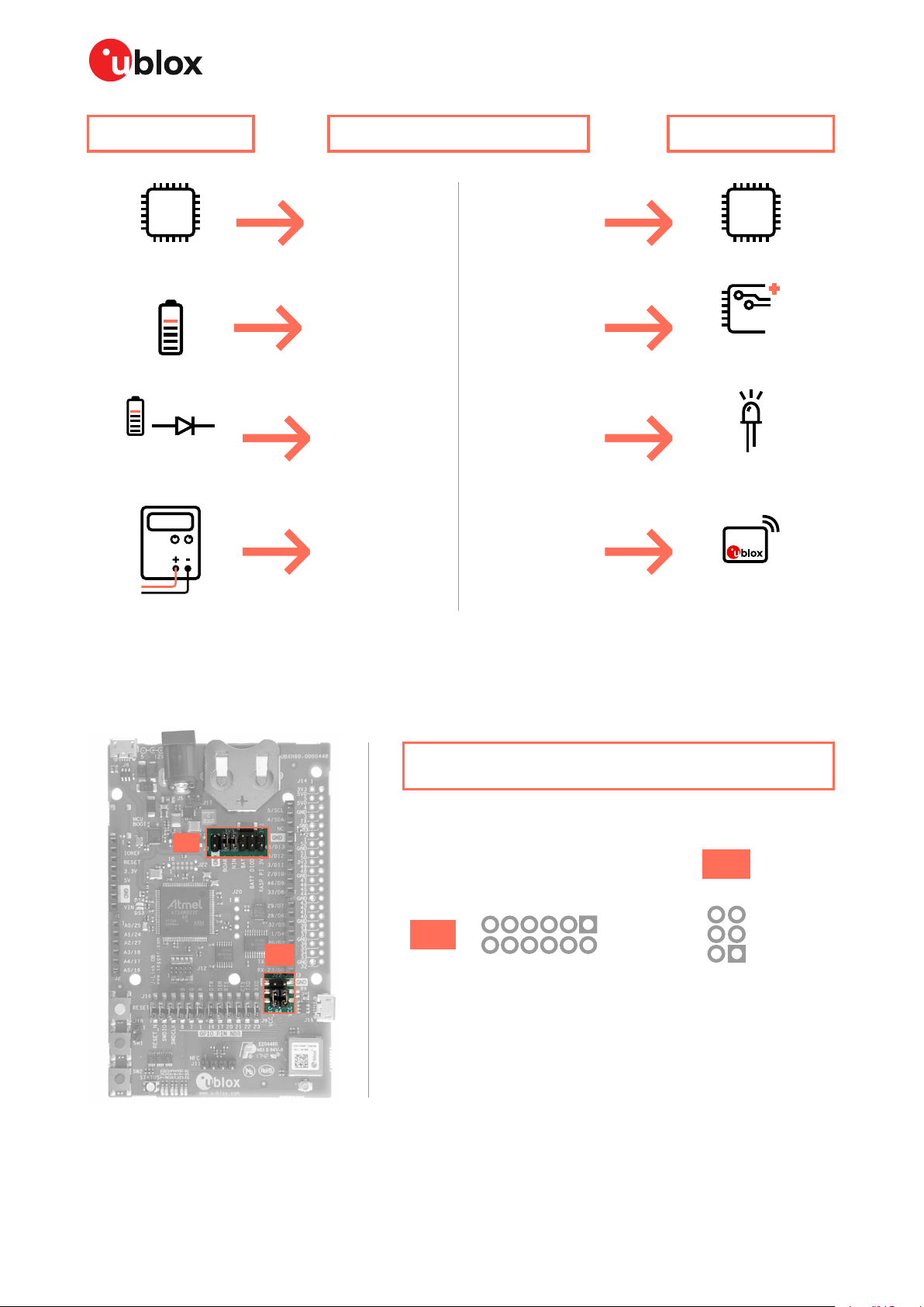
1.2 Kit includes ................................................................................................................................................... 7
1.3 Key features ................................................................................................................................................. 7
1.4 EVK-NINA-B3 block diagram .................................................................................................................... 8
1.5 Connectors ................................................................................................................................................... 9
2 Setting up the evaluation board .................................................................................................. 10
2.1 Evaluation board setup ............................................................................................................................ 10
2.2 Starting up ................................................................................................................................................. 10
EVK-NINA-B31x ................................................................................................................................ 10
EVK-NINA-B30x ................................................................................................................................ 11
2.3 Measuring current consumption ........................................................................................................... 11
Using an ampere meter ................................................................................................................... 11
Using a volt meter ............................................................................................................................. 11
Using an external power supply or power analyzer .................................................................... 12
3 Board configuration ......................................................................................................................... 13
3.1 Powering options ....................................................................................................................................... 13
Selecting the power configuration jumpers ................................................................................ 13
Default power configuration, 3.3 V ............................................................................................... 16
Battery powered, 3 – 1.7 V .............................................................................................................. 17
Battery powered with protection diode, 2.7 – 1.7 V ................................................................... 18
External supply, 3.6 – 1.7 V ............................................................................................................. 19
Raspberry Pi HAT .............................................................................................................................. 20
3.2 Disconnecting NINA signals from board peripherals ........................................................................ 20
4 Interfaces and peripherals ............................................................................................................ 23
4.1 Buttons and LEDs ..................................................................................................................................... 23
4.2 Arduino interface ...................................................................................................................................... 24
Arduino shield compatibility ........................................................................................................... 25
4.3 Raspberry Pi compatible interface ........................................................................................................ 26
Powering considerations ................................................................................................................. 28
UART ................................................................................................................................................... 28
EEPROM support .............................................................................................................................. 29
4.4 Additional Interfaces ................................................................................................................................ 29
Extra memory – external Flash ...................................................................................................... 30
Extra USB to UART interface ......................................................................................................... 31
CPU trace interface .......................................................................................................................... 31
Appendix .................................................................................................................................................... 32
A Schematics ........................................................................................................................................ 32
UBX-17056481 - R07 Page 3 of 41
C1-Public

EVK-NINA-B3 - User guide
B Glossary .............................................................................................................................................. 38
Related documents ................................................................................................................................ 39
Revision history ....................................................................................................................................... 40
Contact ....................................................................................................................................................... 41
UBX-17056481 - R07 Page 4 of 41
C1-Public
EVK-NINA-B3 - User guide
1 Product description
1.1 Overview
The u-blox EVK-NINA-B3 evaluation kit is a versatile development platform that allows quick
prototyping of a variety of extreme low-power Internet of Things (IoT) applications, using full
Bluetooth 5, NFC, and IEEE 802.15.4.
The u-blox EVK-NINA-B3 boards are available in the following variants, depending on the required
antenna and software solution:
• EVK-NINA-B301, with an open CPU NINA-B301 module and an antenna connector for connecting
to external antennas.
• EVK-NINA-B311, with a u-connect NINA-B311 module pre-flashed with u-connectXpress
software, and an antenna connector for connecting to external antennas.
• EVK-NINA-B302, with an open CPU NINA-B302 module that includes an internal antenna (a unique
2.4 GHz metal sheet antenna, soldered onto the module).
• EVK-NINA-B312, with a u-connect NINA-B312 module pre-flashed with u-connectXpress software
and an internal antenna (a unique 2.4 GHz metal sheet antenna soldered onto the module).
• EVK-NINA-B306, with an open CPU NINA-B306 module that includes an internal PCB trace
antenna.
• EVK-NINA-B316, with a u-connect NINA-B316 module pre-flashed with u-connectXpress software
and an internal PCB trace antenna.
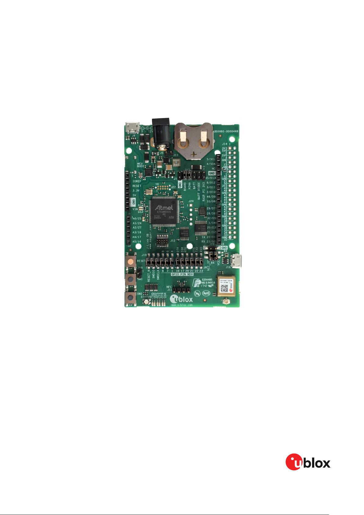
Figure 1: EVK-NINA-B301/-B311 evaluation board
UBX-17056481 - R07 Product description Page 5 of 41
C1-Public
EVK-NINA-B3 - User guide
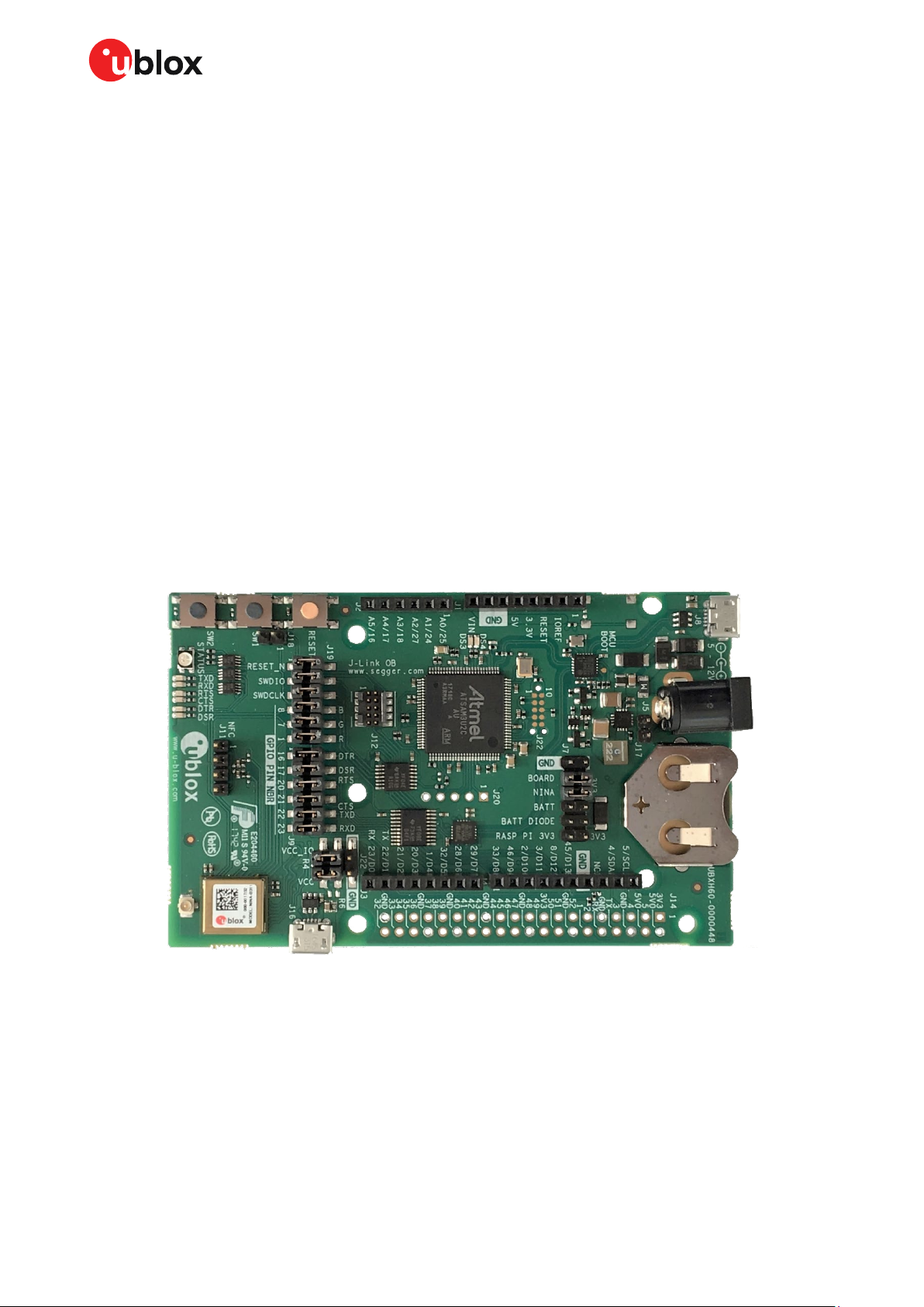
Figure 2: EVK-NINA-B302/-B312 evaluation board
⚠ Take care when handling the EVK-NINA-B302 or EVK-NINA-B312. Applying force to the NINA
module might damage the internal antenna.
Figure 3: EVK-NINA-B306/-B316 evaluation board
The evaluation boards provide access to all the 38 GPIO pins and interfaces available on the
NINA-B3 modules through a variety of connectors and interfaces including Arduino™ Uno R3 [1] and
Raspberry Pi [2] header connectors.
The stand-alone NINA-B3 modules include an Arm
flash and 256 kB RAM, running at a system clock of 64 MHz. This has been integrated inside the
Nordic Semiconductor nRF52840 chip that the modules are based on. The evaulation board provides
simple USB drag-n-drop programming and a SEGGER J-Link debug interface that can be used with
the Open CPU variants of the EVK. Nordic Semiconductors, the manufacturer of the nRF52840 chip
that the NINA-B3 series are based on, provides a free Software Development Kit (SDK) with a broad
selection of drivers, libraries, and example applications that can be used for rapid prototyping.
®
Cortex®-M4F microcontroller with 1 MB internal
UBX-17056481 - R07 Product description Page 6 of 41
C1-Public

EVK-NINA-B3 - User guide
1.2 Kit includes
The EVK-NINA-B3 evaluation kit includes the following:
• NINA-B3 evaluation board
• 2.4 GHz antenna with U.FL connector (only in EVK-NINA-B301 and EVK-NINA-B311)
• NFC antenna
• USB cable
• Quick start card
1.3 Key features
• u-blox NINA-B3 Bluetooth low energy module based on the Nordic nRF52840 chipset
o Full Bluetooth 5 support
o NFC tag functionality
o 802.15.4 PHY
o Integrated Arm Cortex-M4 microcontroller with 1 MB flash, 256 kB RAM, and 64 MHz
system clock
o USB 2.0
o Wide 1.7-3.6 V supply range
• The NINA-B3 module supports different interfaces that can be configured to any of the 38
available GPIO pin(s):
o 8 analog capable inputs
o 12 PWM capable outputs
o 3x SPI
o 2x UART with HW flow control
o 2x I2C
o 1x I2S
o 1x PDM input
o 1x Quadrature decoder
• EVK-NINA-B31x support for u-connectXpress software
• EVK-NINA-B30x support for developing your own software on the Open CPU NINA-B3 module
• Full UART to USB converter with a Virtual COM port, allowing control of the extended UART
features of u-blox u-connectXpress software
• On-board J-Link debugger/programmer
o Mass Storage Device interface to PC for drag-n-drop programming
o Debug port
o An additional Virtual COM port that, for example, may be connected to add-on boards
or to a debug UART on the NINA-B3
• Dedicated USB connector for the NINA-B3 USB interface
• Additional flash memory can be added to the board for use by the NINA-B3 module
• RGB LED and push buttons
• Arduino UNO R3 and Raspberry Pi compatible pin header interfaces
• Jumper headers and level shifters allow for flexible powering options of the NINA-B3 module, even
with full board support. They isolate the module entirely and control each power net separately in
order to precisely measure low power applications or disconnect only unused parts of the board to
save battery life.
• Multiple board power supply options
o 5-12 V power plug
o 5 V USB supply
o 5-12 V Arduino VIN input
• Battery holder supporting CR2032 coin cell batteries
UBX-17056481 - R07 Product description Page 7 of 41
C1-Public
EVK-NINA-B3 - User guide
UART
to USB
USB
conn.
Interface
MCU
(Program &
Debug Unit)
USB
Hub
USB
conn.
Batt.
holder
Power
plug
RF
conn.
Vol tage
Level
Shifters
UART
SWD
Flash
Memory
3.3 V VDD_NINA
DC/DC
reg.
Protect.
diodes
NFC antenna
connector
Dedicated NINA
USB 2.0 conn.
VDD_NINA
Bluetooth
8 0 2 . 15 . 4
Arduino Uno R3 interface
D0D1D2D3D4D5D6
D7
D8D9D10
D11
D12
D13
SCL
SDA
A0
A1
A2
A3
A4
A5
IOREF
3V3
5V
VIN
GND
RESET
ADC/Comp.
GPIO/Dig. Interface GPIO/Dig. Interface
UART
GPIO/Dig. Int.
UART
SW2
Raspberry Pi 40 pin GPIO header
3V3
5V
GND
GPIO/Digital Interface
UART
ID_SC
ID_SD
RPi_3
RPi_4
RPi_5
RPi_6
RPi_7
RPi_2
RPi_8
RPi_9
RPi_10
RPi_11
RPi_12
RPi_13
RPi_14
RPi_15
RPi_16
RPi_17
RPi_18
RPi_19
RPi_20
RPi_21
RPi_22
RPi_23
RPi_24
RPi_25
RPi_26
RPi_27
NINA
Module
User
RGB LED
User
buttons
Reset
button
NINA
SWD conn.
NINA signal
jumper header
SWD
UART
UART
COM port
pin header
Power selector
jumper headers
USB
USB
USB
3.3 V
3.3 V
QSPI
20-pin Trace
connector
ETM/ITM
Trace
USB
NFC
RF
VBUS
VBUS
CR2032
3 V
5 - 12 V
NINA COM port
NINA program & debug
Additional COM port
1. 7 - 3 . 6 V
Raspberry Pi pin
NINA Open CPU function
NINA Open CPU function
Arduino pin
NINA Connectivity Software function
NINA Connectivity Software function
1.4 EVK-NINA-B3 block diagram
The block diagram in Figure 4 shows the major interfaces and internal connections of the EVK-NINAB3. The following sections describe in detail how the different interfaces are connected and may be
used, as well as how the evaluation board may be configured to suit the needs of the user.
Figure 4: EVK-NINA-B3 block diagram
UBX-17056481 - R07 Product description Page 8 of 41
C1-Public
EVK-NINA-B3 - User guide
J5
2
1
1 4
GNDVIN
5 - 12 V
NFC1
GND
GND
NFC2
U.FL RF coax
GND
GND
N/C
VDD_IO
GND
SWDIO
SWDCLK
GPIO_8
N/C
RESET_N
BT1
J17
Power
J8
J16
USB
Debug
J12
Antennas
J11
J10
CR2032
+
3V
2
1
10
9
Micro USB
Micro USB
J17
Debug
Power
Antennas
USB
USB
J8
J5
BT1
J12
J16
J10
J11
Board Connectors
1.5 Connectors
Figure 5 shows the available connectors of the EVK-NINA-B3 and their layout. Table 1 describes the
connectors and their uses in detail.
Figure 5: Available connectors and their pinout
Connector
annotation
J5 Power supply 2.1 mm power jack, the center pin is the positive terminal. 5 – 12 V input.
J17 Power supply Pin header that can be used to connect external power supplies. 5 – 12 V input.
BT1 Battery holder CR2032 coin cell battery holder. CR2032 usually has a 3 V potential when fully
J11 NFC antenna
J10 2.4 GHz RF antenna
J12 Cortex Debug
J8 Power supply, COM
J16 Power supply and
Table 1: EVK-NINA-B3 connector description
UBX-17056481 - R07 Product description Page 9 of 41
C1-Public
Function Description
connector
connector
connector
port and debug USB
NINA USB port
charged.
Pin header that connects to the u-blox NFC antenna included in the kit. The antenna
can be mounted in either direction.
U.FL coaxial connector that can be used to connect antennas or RF equipment. This
connector is only included in the EVK-NINA-B301/EVK-NINA-B311.
10-pin, 50 mil pitch connector that can be used to connect external debuggers to the
NINA-B3 module. The NINA-B3 modules support Serial Wire debug (SWD) and Serial
Wire Viewer, but not JTAG debug.
The main USB connector that is used to program, debug, and communicate with the
NINA module. It can also be used to power the entire board.
Additional USB connector directly connected to the NINA-B3 USB interface. Can also
be used to power the entire board.

EVK-NINA-B3 - User guide
2 Setting up the evaluation board
2.1 Evaluation board setup
The EVK-NINA-B311/-B312/-B316 is delivered with the u-connectXpress software installed on the
module.
Before connecting the module, download and install the latest u-blox s-center evaluation software
from the u-blox website.
To use Bluetooth low energy on the EVK-NINA-B301/-B311, connect a 2.4 GHz antenna to the U.FL
antenna connector (J10). The other EVK versions include antennas on the NINA module.
Plug in either an external power supply in the J5 connector or connect to a USB host with a USB cable
attached to the J8 connector. You can also power the evaluation board with a CR2032 coin cell
battery. The NFC antenna can be connected to the J11 connector.
☞ Make sure that the power configuration jumpers are connected according to your use case.
See Section 3.1 for details, the default configuration shown in section 3.1.2 will work for most
use cases.
⚠ Be careful to check polarity before connecting an external power supply to the EVK-NINA-B3
evaluation board. Center conductor is positive (+) and the ring is negative (-).
The operating system will install the correct drivers automatically. The drivers will have to be installed
only the first time you connect the unit to a new computer.
⚠ If the drivers are not installed automatically, download nRF Connect from www.nordicsemi.com to
get the J-Link CDC UART driver.
Two COM ports will automatically be assigned to the unit by Windows:
• The COM port labeled ‘USB Serial Port’ is used to communicate with the NINA module’s UART
interface.
• The COM port labeled ‘JLink CDC UART Port’ can be used as an extra USB to the UART
interface; see section 4.4.2 for more information.
Do the following to view the assigned COM ports on Windows 7:
• Open the Control Panel and click Hardware and Sound.
• Click Device Manager in Devices and Printers. This will open Device Manager window where you
can view the assigned COM ports.
To view the assigned COM ports on Windows 10, right click on the Windows Start button and select
Device Manager.
2.2 Starting up
EVK-NINA-B31x
2.2.1.1 General usage
The EVK-NINA-B31 is delivered with u-connectXpress SW, and contains a secure boot that will only
allow signed SW from u-blox to boot.
Perform the following steps to enable communication with the module:
1. Start the u-blox s-center evaluation software.
2. Use the default baudrate 115200, 8N1 with flow control.
UBX-17056481 - R07 Setting up the evaluation board Page 10 of 41
C1-Public

EVK-NINA-B3 - User guide
You can now communicate with the module using AT commands.
For a list of available AT commands, see the u-connect AT commands manual [5]. To get started with
the basic use case set up of the EVK-NINA-B3 with u-blox u-connect software, see the
u-connectXpress user guide [7].
2.2.1.2 u-connect software
Go to the u-blox support webpage to obtain the latest available firmware. Instructions on reflashing
the EVK-NINA-B3 can be found in the Software section of the NINA-B3 system integration manual [4].
EVK-NINA-B30x
2.2.2.1 Nordic Semiconductor SDK
The EVK-NINA-B30x is delivered without any SW preflashed,
If you would like to use the EVK-NINA-B3 together with Nordic Semiconductor SDK, refer to the
Software section of the NINA-B3 System integration manual [4] that describes how to:
• Create your own board file
• Adapt the examples in the Nordic Semiconductor SDK to use this board file
See also the u-blox short range open CPU github repository [8].
2.2.2.2 Software debug options
You can debug the software using the following two options in EVK-NINA-B3:
• Onboard debug solution available on the USB connector
• Using an external debugger connected to J12 connector
An external debugger connected to the J12 connector is useful when powering the evaluation board
with a CR2032 coin cell battery, or through the J5 external power supply connector. It could also be
useful in a scenario where the debug MCU interface has been disconnected from the
NINA-B3 module using the jumpers on the J19 header. The SEGGER J-Link software [6] is required in
order to debug using the onboard J-Link hardware on the EVK-NINA-B3.
2.3 Measuring current consumption
☞ Before starting the current consumption measurement, go through Chapter 3 and identify
which power configuration you will need and if you need to isolate any NINA signals. The jumper
connecting J22 pins 1 and 3 must be removed in order to be able to measure current
consumption.
Figure 6 shows some suggestions for measuring the current consumption of the NINA-B3 module,
and how to connect the various instruments.
Using an ampere meter
An ampere meter should be connected in series with whatever the power source is and what is being
measured. It is possible to measure current this way both while supplying the NINA module from the
onboard 3.3 V regulator and from an external supply.
Using a volt meter
In order to use a voltmeter to measure current, the EVK must first be modified. Solder a low
resistance, high tolerance, 0402 sized resistor to the footprint labeled R6. This resistor will replace
the jumper normally positioned between J22 pins - 1 and 3, and any current running through, it will
produce a voltage across its terminals. Measure this voltage using the voltmeter and calculate the
current using Ohm’s law.
UBX-17056481 - R07 Setting up the evaluation board Page 11 of 41
C1-Public
EVK-NINA-B3 - User guide
J22
VCC_IO
VCC
1
GND
5
A
J22
VCC_IO
VCC
1
GND
5
A
6
4
R6
J22
VCC_IO
VCC
3
1
V
J22
VCC_IO
VCC
3
1
A
Ampere meter
Volt meter
One channel Two channels
GND GND
Onboard
3.3 V supply
DC/DC
External supply
1.7 - 3.6 V
-.-- V
Using an external power supply or power analyzer
Connect the instrument terminals to the EVK pins, as shown in Figure 6. An ampere meter may be
added in series. Since an external instrument’s voltage can never perfectly match the EVK’s
generated 3.3 V, there will be a very small current leakage whenever a NINA module signal is
connected to an EVK peripheral, typically in the order of 100’s of nano amps. To reduce this leakage,
use a second external power channel to supply the EVK peripherals. This second channel must also
be used to enable PC communication when using NINA supply voltages other than 3.3 V.
Figure 6: Current consumption measuring options
UBX-17056481 - R07 Setting up the evaluation board Page 12 of 41
C1-Public
EVK-NINA-B3 - User guide
Diode protection
3.3 V
DC/DC
Regulator
Fuse
5 V
3.3 V
Diode protection
3 V
2.7 V
J7
Power select
jumper header
J22
NINA power select
jumper header
VDD_NINA
3.3 V
3.3 V
VIN
1.7 - 3.6 V
external supply
J1 and J14
Arduino and
Raspberry Pi
pin headers
VCC
VCC_IO
VDD_IO
NINA
Module
Board
peripherals
BT1
CR2032
3 V
J5
5 - 12 V
J8
5 V
J 16
5 V
J17 pin 2
VIN pin header
5 - 12 V
J1 pin 8
Ardunio VIN pin
5 - 12 V
Diode protection
USB
conn.
Batt.
holder
Power
jack
USB
conn.
3 Board configuration
3.1 Powering options
Power can be supplied to the board in any of the following ways:
• Via any of the USB connectors, J8 or J16
• Using the power jack, J5
• Using the Arduino interface VIN or 5V pin, J1.8 or J1.5
• Using the Raspberry Pi interface 5V pins, J14.2 or J14.4
• Using the pin header J17
• Plugging in a battery to the battery holder BT1
These power supply sources are distributed to the rest of the board as shown in Figure 7.
⚠ Check the jumper positions carefully; if a jumper is connected in a wrong way, it can permanently
Figure 7: Block diagram of the power net distribution
Selecting the power configuration jumpers
The EVK-NINA-B3 offers flexible powering options for the NINA-B3 module and the board itself. To
configure this, jumpers are added or removed to pin headers, shorting two of the pins together and
connecting or disconnecting different power nets on the evaluation board.
Figure 8 provides an overview of the available EVK power sources and shows the schematic net names
to which they are connected.
damage the components that are ON or connected to the board. Also note that some jumpers
should not be mounted simultaneously.
UBX-17056481 - R07 Board configuration Page 13 of 41
C1-Public
EVK-NINA-B3 - User guide
DC/DC
Onboard 3.3 V
converter
Battery
Battery with
protection diode
MCU
PC communication
HAT
Raspberry Pi
expansion board
NINA module power
Board I/O power:
Level shifters, LEDs etc.
3V3
VBAT_DIODE
VBAT
VDD_MCU
3V3_PI
VDD_IO
VCC
VCC_IO
Sources Net names
Targets
Any power net
-.-- V
External supply
iguration
GNDGND
VDD_MCU
VDD_NINA
VDD_NINA
VDD_NINA
3V3_PI
3V3
3V3
VBAT
VBAT_DIODE
3V3
J7
J22
111
12 2
J7
GNDGND
VDD_IO
VCC_IO
VDD_NINA
VCC
5
6
2
1
J22
Power Conf
Figure 8: Available EVK power sources and targets
Figure 9 shows the pinout location of power configuration jumper headers J7 and J22.
Figure 9: Jumper headers J7 and J22
UBX-17056481 - R07 Board configuration Page 14 of 41
C1-Public

EVK-NINA-B3 - User guide
Table 2 describes the pinout of jumper headers J7 and J22 used to configure the board power nets.
Connector
annotation
J7 1 3V3 Regulated 3.3 V net. This net is supplied by the board and will always be
J22 1 VCC NINA module voltage supply that connects to the module VCC pin. Shorted
Table 2: J7 and J22 pin out
Pin
number
2 3V3_PI Connects to the Raspberry Pi header’s (J14) 3V3 pins. If a Raspberry Pi is
3 VBAT_DIO
4 VDD_NINA Connects to J22 pin 3, from where it can be connected to the module supply
5 VBAT Battery + terminal
6 VDD_NINA Connects to J22 pin 3, from where it can be connected to the module supply
7 3V3 Regulated 3.3 V net. This net is supplied by the board and will always be
8 VDD_NINA Connects to J22 pin 3, from where it can be connected to the module supply
9 3V3 Regulated 3.3 V net. This net is supplied by the board and will always be
10 VDD_MCU Supply net for the board functions not directly connected to the NINA
11 GND Ground net.
12 GND Ground net.
2 VCC_IO Connects to the NINA module VCC_IO pin. Shorted to the VCC net via 0 Ω
3 VDD_NINA Connects to J7 pins 4, 6 and 8. Short J22 pins 1 and 3 allow the EVK to
4 VDD_IO Supply net for level shifters, LEDs and peripherals connected directly to the
5 GND Ground net.
6 GND Ground net.
Schematic
net name
DE
Description
powered as long as a power source is connected.
connected, this net must be unconnected to prevent back currents. If a HAT
is connected, this net can be shorted to the EVK 3.3 V supply to power the
HAT.
To protect the battery from current back surges, connect the battery to the
NINA module via a protection diode using this pin.
pin or somewhere else.
pin or somewhere else.
powered as long as a power source is connected.
pin or somewhere else.
powered as long as a power source is connected.
module; Interface MCU, USB hub, UART to USB converter etc.
to the VCC_IO net via 0 Ω resistor R4 by default.
resistor R4 by default.
power the NINA module.
NINA module. Short J22 pins 2 and 4 use the NINA module I/O voltage as
supply.
UBX-17056481 - R07 Board configuration Page 15 of 41
C1-Public

EVK-NINA-B3 - User guide
J7
BOARD
NINA
3V3
34
2 1
J22
VCC_IO
VCC
7
8
9
10
NINA module powerboard I/O power
J22: 2-4 J22: 1-3
PC communication
MCU
DC/DC
EVB powered
J7: 9-10J7: 7-8
Default power configuration, 3.3 V
This is the default power configuration for the evaluation board, and the jumpers are installed out of
the box with this power configuration. All board peripherals are powered up, the NINA module is
directly supplied by the board and everything is running at 3.3 V.
Figure 10: Jumper positions for default power configuration
Connector
annotation
J7 7, 8 Selects the board regulated 3.3 V net as source for the VDD_NINA net.
J22 1, 3 Powers up the NINA module. The NINA VCC and VCC_IO pins are connected to the selected
Table 3: Jumper positions for default power configuration
Add jumper
to pins
9, 10 Powers up the Interface MCU, USB hub, and UART to USB converter with 3.3 V.
2, 4 Powers up the peripherals directly connected to NINA such as LEDs and external memory with
Description
source for the VDD_NINA net.
the NINA supply voltage.
UBX-17056481 - R07 Board configuration Page 16 of 41
C1-Public

EVK-NINA-B3 - User guide
J7
BOARD
BATT
3V3
34
2 1
J22
VCC_IO
VCC
5
6
9
10
NINA module powerboard I/O power
(optional)
J22: 2-4 J22: 1-3
PC communication
(optional)
MCU
J7: 9-10
Battery powered
J7: 5-6
Battery powered, 3 – 1.7 V
Figure 11 shows the default configuration for battery-powered operation, where the jumpers
highlighted with dashed lines are optional.
The battery voltage is connected to VDD_NINA, which in turn, is connected to the NINA-B3 VCC
supply. If needed, a jumper can be added to J22 pins - 2 and 4 to supply LEDs and other peripherals
with power – as long as this does not exceed the maximum current rating of the battery. If the NINA
module has to be configured, the VDD_MCU net can be connected to enable PC communications by
adding a jumper to the J7 pins 9 and 10.
☞ Jumpers must be connected to both J7: 9-10 and J22: 2-4 to be able to communicate with the
NINA module from a PC. If possible, the EVB power configuration should be switched to the
default 3.3 V configuration, as connecting an extra board peripheral might deplete the battery.
⚠ Do not connect jumpers J7: 5-6 and J7: 7-8 at the same time while a battery is connected! This
might cause damage to the battery.
Figure 11: Jumper positions for battery powered operation (jumpers shown with dashed lines are optional)
Connector
annotation
J7 5, 6 Selects the battery connected to the battery holder as source for the VDD_NINA net.
J22 1, 3 Powers up the NINA module. The NINA VCC and VCC_IO pins are connected to the selected
Table 4: Jumper positions for battery powered operation (two optional jumpers)
UBX-17056481 - R07 Board configuration Page 17 of 41
C1-Public
Add jumper
to pins
9, 10 (Optional) Powers up the Interface MCU, USB hub, and UART to USB converter with 3.3 V.
2, 4 (Optional) Powers up the peripherals directly connected to NINA such as LEDs and external
Description
source for the VDD_NINA net.
memory with the NINA supply voltage.

EVK-NINA-B3 - User guide
J7
BOARD
BATT DIODE
3V3
34
2 1
J22
VCC_IO
VCC
3
4
9
10
NINA module powerboard I/O power
(optional)
J22: 2-4 J22: 1-3
PC communication
(optional)
MCU
J7: 9-10
J7: 3-4
Battery powered
with protection
Battery powered with protection diode, 2.7 – 1.7 V
This use case is meant to protect the battery from current back surges. When using the NFC
interface, there is a risk that the applied electromagnetic field can cause back surges on the module
power supply lines that typically damage a non-chargeable battery. To prevent this potential damage,
a schottky diode is added in series with the battery to block any back current surges.
Figure 12 shows the jumper configuration for connecting the diode for battery-powered operation,
where the jumper is added to J7 pins 3 and 4 instead of pins 5 and 6. The jumpers shown in dashed
lines are optional.
☞ The diode will lower the voltage level of the battery by about 0.3 V.
Figure 12: Jumper positions for battery powered operation using the protection diode
Connector
annotation
J7 3, 4 Selects the diode protected battery as a source for the VDD_NINA net.
J22 1, 3 Powers up the NINA module. The NINA VCC and VCC_IO pins are connected to the selected
Table 5: Jumper positions for battery powered operation with a protection diode (two optional jumpers)
UBX-17056481 - R07 Board configuration Page 18 of 41
C1-Public
Add jumper
to pins
9, 10 (Optional) Powers up the Interface MCU, USB hub, and UART to USB converter with 3.3 V.
2, 4 (Optional) Powers up the peripherals directly connected to NINA such as LEDs and external
Description
source for the VDD_NINA net.
memory with the NINA supply voltage.

EVK-NINA-B3 - User guide
J7
BOARD
NINA
3V3
34
J22
7
8
9
10
board I/O power
(optional)
J22: multiple
PC communication
(optional)
MCU
DC/DC
EVB powered
(optional)
J7: 9-10J7: 7-8
VCC_IO
VCC
12
56
GND
-.-- V
External supply
External supply, 3.6 – 1.7 V
When measuring current consumption or performing other NINA-B3 module characterization
measurements, it can be useful to power the module with an external source such as a lab power
supply. In such a case, all jumpers can be removed and the required supply nets can be fed externally
by connecting to the pin headers. For example, the NINA-B3 module can be powered by connecting an
external supply directly to the J22 pin 1 and GND. See section 2.3 for more information on how to
connect external power supplies.
☞ Make sure that unpowered parts of the board are properly isolated from the NINA module. If a
voltage is applied to the signal of an unpowered device/component, current might leak through
various protection circuits of this device. This might give false readings when measuring
current consumption etc. Isolation can be achieved by removing NINA signal jumpers (see
section 3.2) for example.
Figure 13 below shows a few optional jumper connections that can be helpful when supplying the
module with an external supply.
Figure 13: Optional jumper positons while using an external power supply
Table 6 shows the optional jumper positions for configuring the power up behavior of the board when
using an external supply.
Connector
annotation
J7 7, 8 (Optional) Selects the board-regulated 3.3 V net as a source for the VDD_NINA net.
J22 3, 4 (Optional) Powers up the peripherals directly connected to NINA such as LEDs and external
Table 6: Optional jumper positions for use with an external supply
UBX-17056481 - R07 Board configuration Page 19 of 41
C1-Public
Add jumper
to pins
9, 10 (Optional) Powers up the Interface MCU, USB hub, and UART to USB converter with 3.3 V.
Description
memory with the selected source for the VDD_NINA net.

EVK-NINA-B3 - User guide
J7
BOARD
RASP PI 3V3
3V3
34
2 1
J22
VCC_IO
VCC
1
2
9
10
NINA module powerboard I/O power
(optional)
J22: 2-4 J22: 1-3
PC communication
(optional)
MCU
J7: 9-10
NINA
7
8
DC/DC
EVB powered
J7: 7-8
HAT
Raspberry Pi
expansion board
J7: 1-2
3V3
Raspberry Pi HAT
Use the jumper configurations shown in Figure 14 to connect a HAT to the Raspberry Pi interface.
Depending on how the NINA module should communicate with a test PC over USB or with the HAT,
the VDD_MCU net could be left unpowered. The jumpers shown in dashed lines are optional.
⚠ The 3V3_PI supply net must only be powered when connecting to a Raspberry Pi expansion board
(HAT). The jumper (J7: 1-2) must be disconnected if you are connecting to a Raspberry Pi board.
Figure 14: Configuration for Raspberry Pi HAT connection (optional jumpers shown with dashed lines)
Connector
annotation
J7 1,2 Connects the 3V3_PI net to the regulated 3.3 V supply.
J22 1, 3 Powers up the NINA module. The NINA VCC and VCC_IO pins are connected to the selected
Table 7: Jumper configuration when connected to a Raspberry Pi HAT
Add jumper
to pins
7, 8 Selects the board regulated 3.3 V net as a source for the VDD_NINA net.
9, 10 (Optional) Powers up the Interface MCU, USB hub, and UART to USB converter with 3.3 V.
2, 4 (Optional) Powers up the peripherals directly connected to NINA such as LEDs and external
Description
source for the VDD_NINA net.
memory with the NINA supply voltage.
3.2 Disconnecting NINA signals from board peripherals
All evaluation board peripherals, such as level shifters, LEDs, and the interface MCU are connected to
the NINA-B3 module by default. This might not suit all evaluation scenarios.
All peripherals can be switched off by disconnecting their power supplies (see section 3.1), but if only
specific signals have to be isolated, it will require finer control. All the NINA module signals that are
connected to board peripherals have thus been routed via jumper headers, so that jumpers can be
pulled or added as needed by the evaluation board user, isolating, or connecting specific signals.
Figure 15 shows the physical layout of these jumper headers.
UBX-17056481 - R07 Board configuration Page 20 of 41
C1-Public

EVK-NINA-B3 - User guide
J9
J19
J9
J19
12
11
2
1
12
11
2
1
RESET_MCURESET_N
SWDIO
SWDCLK
GPIO_8
GPIO_7
GPIO_1
GPIO_16
GPIO_17
GPIO_20
GPIO_21
GPIO_22
GPIO_23
SWDIO_MCU
SWDCLK_MCU
RGB_BLUE
RGB_GREEN
RGB_RED
UART DTR
UART DSR
UART RTS
UART CTS
UART TXD
UART RXD
NINA Signal Jumper Headers
Figure 15: Jumper headers J19 and J9 used to isolate specific NINA signals
Table 8 describes the pinout for the jumper headers, J19 and J9, used for isolating or connecting
specific evaluation board peripherals that are connected to the NINA-B3 module by default.
Connector
annotation
J19 1 RESET_N NINA reset signal, active low
J9 1 GPIO_16/
Pin number Schematic net name Description
2 RESET_N_I Connects to the Interface MCU’s reset line
3 SWDIO SWD data signal
4 SWDIO_I Interface MCU SWD data signal, used to program/debug the NINA
module
5 SWDCLK SWD clock signal
6 SWDCLK_I Interface MCU SWD data signal, used to program/debug the NINA
module
7 GPIO_8 NINA-B30: GPIO or TRACE
NINA-B31: BLUE signal
8 BLUE RGB diode blue signal, active low
9 GPIO_7/
SWITCH_1
10 GREEN RGB diode green signal, active low
11 GPIO_1 NINA-B30: GPIO, can be used as user LED output
12 RED RGB diode red signal, active low
UART_DTR
2 UART_DTR_I UART to USB DTR signal
3 GPIO_17/
UART_DSR
4 UART_DSR_I UART to USB DSR signal
5 GPIO_20/
UART_RTS
NINA-B30: GPIO, can be used as either user LED output or push-button
input
NINA-B31: SWITCH_1 and GREEN signal
NINA-B31: RED signal
NINA-B30: analog capable GPIO signal
NINA-B31: UART DTR output
NINA-B30: analog capable GPIO signal
NINA-B31: UART DSR input
NINA-B30: analog capable GPIO signal
NINA-B31: UART RTS output
UBX-17056481 - R07 Board configuration Page 21 of 41
C1-Public

EVK-NINA-B3 - User guide
Connector
annotation
Table 8: Pinout of the jumper headers - J19 and J9
Pin number Schematic net name Description
6 UART_RTS_I UART to USB RTS signal
7 GPIO_21/
UART_CTS
8 UART_CTS_I UART to USB CTS signal
9 GPIO_22/
UART_TXD
10 UART_TXD_I UART to USB TXD signal
11 GPIO_23/
UART_RXD
12 UART_RXD_I UART to USB RXD signal
NINA-B30: GPIO signal
NINA-B31: UART CTS input
NINA-B30: GPIO signal
NINA-B31: UART TXD output
NINA-B30: analog capable GPIO signal
NINA-B31: UART RXD input
UBX-17056481 - R07 Board configuration Page 22 of 41
C1-Public

EVK-NINA-B3 - User guide
☞
SW0
SW1
SW2
DS6
DS5
DS1
DS2
DS7
DS8
DS9
DS3
DS4
Buttons and LEDs
SW0
Reset
User button
User button
SW1
SW2
DS3
Interface MCU LED
Interface MCU LED
Status LED
DS4
TXD LED
RXD LED
RTS LED
CTS LED
DTR LED
DSR LED
DS9
DS8
DS7
DS2
DS1
DS5
DS6
4 Interfaces and peripherals
4.1 Buttons and LEDs
Figure 16: Position of the push buttons and LEDs on the evaluation board
Annotation Function Description
SW0 Reset button Connected directly to the NINA RESET_N pin.
SW1 User button Push button for application use. Connected directly to the NINA SWITCH_1 (GPIO_7) pin
SW2 User button Push button for application use. Connected directly to the NINA SWITCH_2 (GPIO_18)
pin.
Table 9: EVK-NINA-B3 buttons
Annotation Function Description Color
DS1 UART CTS LED Connected to the NINA UART_CTS (GPIO_21) pin via jumper header J9 Green
DS2 UART RTS LED Connected to the NINA UART_RTS (GPIO_20) pin via jumper header J9 Orange
DS3 Interface MCU LED Blinks on USB enumeration and activity, lit when the Interface MCU is
connected via USB
DS4 Interface MCU LED Error LED Orange
DS5 UART DTR LED Connected to the NINA UART_DTR (GPIO_16) pin via jumper header J9 Orange
DS6 UART DSR LED Connected to the NINA UART_DSR (GPIO_17) pin via jumper header J9 Green
DS7 UART TXD LED Connected to the NINA UART_TXD (GPIO_22) pin via jumper header J9 Orange
DS8 UART RXD LED Connected to the NINA UART_RXD (GPIO_23) pin via jumper header J9 Green
DS9 RGB LED Connected to the NINA RED (GPIO_1), GREEN (GPIO_7) and BLUE (GPIO_8)
Table 10: EVK-NINA-B3 LED indicators
pins via jumper header J19. The RGB LED shows the status for the uconnect applications.
See the NINA-B3 data sheet [3] for additional information.
UBX-17056481 - R07 Interfaces and peripherals Page 23 of 41
C1-Public
Green
RGB

EVK-NINA-B3 - User guide
J1
J2
J3
J4
Mounting Holes
Arduino Interface
J1
1
8
N/C
VDD_IO
RESET_N
3V3
5 V
GND
GND
VIN
J2
1
6
A0/GPIO_25
A1/GPIO_24
A2/GPIO_27
A3/GPIO_18
A4/GPIO_17
A5/GPIO_16
J3
1
8
D5/GPIO_32
D4/GPIO_1
D3/GPIO_20
D2/GPIO_21
TX/D1/GPIO_22
RX/D0/GPIO_23
D6/GPIO_28
D7/GPIO_29
J4
1
10
SCL/GPIO_5
SDA/GPIO_4
N/C
GND
D13/GPIO_45
D12/GPIO_8
D11/GPIO_3
D10/GPIO_2
D9/GPIO_46
D8/GPIO_33
4.2 Arduino interface
The EVK-NINA-B3 includes a set of pin headers and mounting holes that are compatible with certain
Arduino or Arduino inspired shields. Figure 17 shows the layout of the Arduino interface and Table 11
explains the pinout in more detail. Section 4.2.1 describes what specifications must be met for a
shield to be compatible for use with the EVK-NINA-B3.
Figure 17: Pin headers that are compatible with some Arduino shields
Conn. Pin
J1 1 N/C Not Connected - - Not connected
Arduino
No.
pin
2 IOREF I/O reference voltage level.
3 RESET NINA reset signal input. Active low
4 3.3V 3.3 V DC regulated supply output 3V3 -
5 5V 5 V regulated supply output 5V - Cannot be used as supply input, use
Description Schematic
Selectable by user to 1.7 – 3.6 V
logic
net name
VDD_IO - See section 3.1
RESET_N P0.18
nRF52
pin
6 GND Ground GND GND
7 GND Ground GND GND
8 VIN External DC supply input, 5 – 12 VDC VIN -
J2 1 A0 Analog input GPIO_25 P0.04 Analog function capable GPIO
UBX-17056481 - R07 Interfaces and peripherals Page 24 of 41
C1-Public
Alternate functions and notes
VIN instead. Only supplied by USB
VBUS.

EVK-NINA-B3 - User guide
Conn. Pin
J3 1 D0/RX Digital I/O, UART RX UART_RXD/
J4 1 D8 Digital I/O GPIO_33 P1.09
Table 11: Pinout of the Arduino UNO R3 compatible interface
Arduino
No.
pin
2 A1 Analog input GPIO_24 P0.30 Analog function capable GPIO
3 A2 Analog input GPIO_27 P0.05 Analog function capable GPIO
4 A3 Analog input SWITCH_2/
5 A4 Analog input UART_DSR/
6 A5 Analog input UART_DTR/
2 D1/TX Digital I/O, UART TX UART_TXD/
3 D2 Digital I/O UART_CTS/
4 D3 Digital I/O UART_RTS/
5 D4 Digital I/O GPIO_1 P0.13
6 D5 Digital I/O GPIO_32 P0.11
7 D6 Digital I/O GPIO_28 P0.09 Signal not connected by default.
8 D7 Digital I/O GPIO_29 P0.10 Signal not connected by default.
2 D9 Digital I/O GPIO_46 P0.12
3 D10 Digital I/O GPIO_2 P0.14
4 D11 Digital I/O GPIO_3 P0.15
5 D12 Digital I/O GPIO_8 P1.00
6 D13 Digital I/O GPIO_45 P0.07
7 GND Ground GND
8 AREF Analog reference voltage level - - Not connected
9 SDA I2C data signal GPIO_4 P0.16
10 SCL I2C clock signal GPIO_5 P0.24
Description Schematic
net name
GPIO_18
GPIO_17
GPIO_16
GPIO_23
GPIO_22
GPIO_21
GPIO_20
nRF52
pin
P0.02 Analog function capable GPIO,
P0.28 Analog function capable GPIO,
P0.03 Analog function capable GPIO,
P0.29 UART_RXD signal on NINA-B31
P1.13 UART_TXD signal on NINA-B31
P1.12 UART_CTS signal on NINA-B31
P0.31 UART_RTS signal on NINA-B31
Alternate functions and notes
SWITCH_2 on NINA-B31.
This signal is pulled low when the
button SW2 is pressed.
UART_DSR signal on NINA-B31
UART_DTR signal on NINA-B31
Configured for NFC use.
Configured for NFC use.
Arduino shield compatibility
☞ The EVK-NINA-B3 has an I/O voltage range of 1.7-3.6 V. It can therefore be used only with
shields that also support an I/O voltage within this range.
The EVK-NINA-B3 has a pinout that is compatible with some Arduino, or Arduino inspired, shields.
This section describes the features of certain EVK pins that a shield must comply with:
• IOREF: The I/O voltage level of the NINA-B3 module is 3.3 V by default, but the EVK can be modified
to allow other voltages (1.7-3.6 V).
• RESET: Is connected to the RESET button (SW0).
• 3.3 V: A regulated 3.3 V output. Should not be used as a voltage supply input, use the VIN pin
instead.
UBX-17056481 - R07 Interfaces and peripherals Page 25 of 41
C1-Public

EVK-NINA-B3 - User guide
• 5 V: Is only a 5 V supply output if the EVK is being powered by USB. If any other power configuration
is used, this pin will be unconnected (floating). It is safe to connect an external 5 V supply to this
pin even when a USB cable is connected. This pin may be used to power the board.
• VIN: May be used as a 5 -12 V supply input to power the EVK-NINA-B3.
• Pin 0 (RX): Is connected to the NINA-B3 UART RX pin (NINA pin 23).
• Pin 1 (TX): Is connected to the NINA-B3 UART TX pin (NINA pin 22).
Note on SCL/SDA: On some Arduino boards, the I
2
C signals, SCL, and SDA are connected to the pins
A4 and A5 and to the SCL and SDA pins in the top right hand corner. Since these pins will be shorted
together it might cause problems when connected to the EVK-NINA-B3, which has not shorted these
pins together.
Note on digital I/O pins: Some of the digital I/O pins can be connected to the on-board debug MCU,
thus allowing serial communication and flashing/debugging over USB. This can cause interference on
the signals that are also used by an Arduino shield, see section 3.2 on how to disconnect these signals
from the debug MCU.
4.3 Raspberry Pi compatible interface
The EVK-NINA-B3 includes a 40-pin GPIO header that can be used to interface with either a Raspberry
Pi computer board or with a Raspberry Pi expansion board (HAT). The EVK-NINA-B3 uses different
hardware and software configurations depending on if it is connected to a Pi or a HAT; the differences
are covered in this section. The default configuration is to connect to a Pi.
Not all the Raspberry Pi versions and HATs are supported, since it requires the 40-pin GPIO header,
which older versions did not have. Table 12 lists the compatible Raspberry Pi versions.
Compatible Raspberry Pi boards
Raspberry Pi 1 Model A+
Raspberry Pi 1 Model B+
Raspberry Pi 2 Model B
Raspberry Pi 3 Model B
Raspberry Pi Zero
Raspberry Pi Zero W
Table 12: Compatible Raspberry Pi boards
Figure 18 shows the layout of the Raspberry Pi interface and Table 13 explains the pinout in detail.
There are three mounting holes that can be used for increased mechanical stability. The two holes on
either side of connector J14 are common to all Raspberry Pi boards, but the third one is only
compatible with the Pi Zero boards.
UBX-17056481 - R07 Interfaces and peripherals Page 26 of 41
C1-Public

EVK-NINA-B3 - User guide
J14
MOUNTING HOLES
Raspberry Pi Interface
3V3_PI
GPIO_5
GPIO_4
GPIO_3
GND
GPIO_2
GPIO_52
GPIO_51
3V3_PI
GPIO_48
GPIO_47
GPIO_45
GND
GPIO_42
GPIO_40
GPIO_39
GPIO_37
GPIO_36
GPIO_34
GND
5 V
5 V
GND
RASP_T XD
RASP_RXD
GPIO_1
GND
GPIO_50
GPIO_49
GND
GPIO_46
GPIO_44
GPIO_43
GPIO_41
GND
GPIO_38
GND
GPIO_35
GPIO_33
GPIO_32
J14
2
1
39 40
PULL-UP RESISTORS
R63
R62
R57
R58
R59
R60
UART RESISTORS
R44
R50
Figure 18: Pin header J14 that is compatible with the Raspberry Pi GPIO connectors
Conn. Pin
J14 1 3.3 V 3.3 V supply pin 3V3_PI - Not connected by default. See section 3.1.
UBX-17056481 - R07 Interfaces and peripherals Page 27 of 41
C1-Public
No.
Raspberry
Pi pin
Description Schematic
net name
nRF52
pin
Alternate functions and notes
2 5 V 5 V supply pin 5V - Cannot be used as supply input. Supplied
by USB VBUS and protected from back
powering.
3 GPIO02 Digital I/O GPIO_5 P0.24
4 5 V 5 V supply pin 5V - Cannot be used as supply input. Supplied
by USB VBUS and protected from back
powering.
5 GPIO03 Digital I/O GPIO_4 P0.16
6 GND Ground GND GND
7 GPIO04 Digital I/O GPIO_3 P0.15
8 GPIO14 Digital I/O, UART TX/RX RASP_TXD P0.29 Connected to NINA UART_RXD pin by
9 GND Ground GND GND
10 GPIO15 Digital I/O, UART RX/TX RASP_RXD P1.13 Connected to NINA UART_TXD pin by
11 GPIO17 Digital I/O GPIO_2 P0.14
12 GPIO18 Digital I/O GPIO_1 P0.13
13 GPIO27 Digital I/O GPIO_52 P0.19 Connected to NINA through a solder bridge.
14 GND Ground GND GND
15 GPIO22 Digital I/O GPIO_51 P0.17 Connected to NINA through a solder bridge.
default. See section 4.3.2.
default. See section 4.3.2.
If the solder bridge is cut this pin is left
floating.
If the solder bridge is cut this pin is left
floating.

EVK-NINA-B3 - User guide
Conn. Pin
Table 13: Pinout of the Raspberry Pi compatible interface
Raspberry
No.
Pi pin
16 GPIO23 Digital I/O GPIO_50 P0.20 Connected to NINA through a solder bridge.
17 3.3 V 3.3 V supply pin 3V3_PI - Not connected by default. See section 3.1.
18 GPIO24 Digital I/O GPIO_49 P0.22 Connected to NINA through a solder bridge.
19 GPIO10 Digital I/O GPIO_48 P0.21 Connected to NINA through a solder bridge.
20 GND Ground GND GND
21 GPIO09 Digital I/O GPIO_47 P0.23 Connected to NINA through a solder bridge.
22 GPIO25 Digital I/O GPIO_46 P0.12
23 GPIO11 Digital I/O GPIO_45 P0.07
24 GPIO08 Digital I/O GPIO_44 P0.27
25 GND Ground GND GND
26 GPIO07 Digital I/O GPIO_43 P0.06
27 ID_SD EEPROM config I2C data
28 ID_SC EEPROM config I2C clock
29 GPIO05 Digital I/O GPIO_40 P1.15
30 GND Ground GND GND
31 GPIO06 Digital I/O GPIO_39 P1.11
32 GPIO12 Digital I/O GPIO_38 P1.10
33 GPIO13 Digital I/O GPIO_37 P1.03
34 GND Ground GND GND
35 GPIO19 Digital I/O GPIO_36 P1.02
36 GPIO16 Digital I/O GPIO_35 P1.01
37 GPIO26 Digital I/O GPIO_34 P1.08
38 GPIO20 Digital I/O GPIO_33 P1.09
39 GND Ground GND GND
40 GPIO21 Digital I/O GPIO_32 P0.11
Description Schematic
signal
signal
nRF52
net name
GPIO_42 P0.26 Should only be used to read or simulate
GPIO_41 P1.14 Should only be used to read or simulate
pin
Alternate functions and notes
If the solder bridge is cut this pin is left
floating.
If the solder bridge is cut this pin is left
floating.
If the solder bridge is cut this pin is left
floating.
If the solder bridge is cut this pin is left
floating.
HAT EEPROMs. See section 4.3.3.
HAT EEPROMs. See section 4.3.3.
Powering considerations
There are two voltage nets used in the Raspberry Pi interface - 3V3_PI and 5V. Both the 3V3_PI and
5V nets can be used to power HATs, but should not be used when connecting to a Raspberry Pi. For
more information, see section 3.1.6.
⚠ The 3V3_PI power net must not be connected to the 3.3 V supply when connected to a Raspberry
Pi board. It could damage both the boards.
UART
The Raspberry Pi interface provides two pins that can be used for UART communications GPIO14 and
GPIO15. In UART communications, signals are always connected RX <-> TX and vice versa. This
means that on a Raspberry Pi board GPIO14 will be TX and on a HAT it will be RX. To support talking
UBX-17056481 - R07 Interfaces and peripherals Page 28 of 41
C1-Public

EVK-NINA-B3 - User guide
J20
UART
U10
C54
Flash Memory
VDD_IO
QSPI_D3
QSPI_CLK
QSPI_D0
U10
GND
CTS
RTS
RXD
TXD
1
J20
5
346
5
8
7
TRACE_D1
TRACE_D2
TRACE_D0
TRACE_D3
TRACE_CLK
GND
GND
GND
N/C
N/C
J21
TRACE_D0
N/C
SWDCLK
RESET_N
SWDIO
GND
N/C
GND
GND
VDD_IO
19
20
1
2
Additional Interfaces
Trace
J21
QSPI_D2
QSPI_D1
GND
QSPI_CS
External Flash
Debug and Trace
UART
1
2
to both HATs and Pi boards, the zero Ω resistors - R57, R58, R59 and R60 can be used to toggle the
NINA TX and RX pins between GPIO14 and GPIO15. If a NINA-B30 is used, this switch can also be
made in the software. By default, the EVK-NINA-B3 will be configured to simulate a HAT, and GPIO14
is connected to the NINA UART_RXD pin and GPIO15 is connected to the NINA UART_TXD pin.
EEPROM support
The Raspberry Pi interface supports a unique EEPROM solution to store the HAT specific GPIO
configurations on the HAT board, to be read by the Raspberry Pi before configuring its GPIOs. The two
pins used for this - ID_SD and ID_SC, are connected to the NINA-B3 module. The NINA module can
thus either read the GPIO configuration from a HAT, or simulate an EEPROM and send configurations
to a connected Pi. This requires a NINA-B30 module and a custom built application.
It is not mandatory to use this EEPROM solution; if not used, the two NINA pins GPIO_42 and GPIO_41
should be left unconfigured.
Two pull-up resistors - R44 and R50, can be added to the I
the evaluation board by default.
2
C lines if needed. They are not mounted on
Visit https://github.com/raspberrypi/hats/blob/master/designguide.md
for more information on the
ID EEPROM specification.
4.4 Additional Interfaces
In addition to the normal interfaces most commonly used, there are a few expansion options available
for the user. These extra interfaces require some modifications of the EVB before they can be used.
Figure 19 shows the additional interfaces – that require some soldering before use.
Figure 19: Additional interfaces and expansion options
Connector
annotation
Pin
number
Schematic net name nRF52 pin Description
U10 1 QSPI_CS/GPIO_51 P0.17 Chip select input signal, active low
2 QSPI_D1/GPIO_48 P0.21 MISO in single SPI mode, or data I/O signal in dual/quad mode
3 QSPI_D2/GPIO_49 P0.22 Data I/O signal in quad mode (optional)
UBX-17056481 - R07 Interfaces and peripherals Page 29 of 41
C1-Public

EVK-NINA-B3 - User guide
Connector
annotation
J20 1 MCU_TXD - Interface MCU data output signal
J21 1 VDD_IO - Supply net for LEDs and peripherals connected directly to the
Table 14: Pinout of the additional interfaces
Pin
number
4 GND GND Ground
5 QSPI_D0/GPIO_50 P0.20 MOSI in single SPI mode, or data I/O signal in dual/quad mode
6 QSPI_CLK/GPIO_52 P0.19 Chip clock input signal, up to 32 MHz supported
7 QSPI_D3/GPIO_47 P0.23 Data I/O signal in quad mode (optional)
8 VDD_IO - Supply net for LEDs and peripherals connected directly to the
2 MCU_RXD - Interface MCU data input signal
3 MCU_RTS - Interface MCU flow control output signal
4 MCU_CTS - Interface MCU flow control input signal
5 GND GND Ground
2 SWDIO SWDIO Serial Wire Debug data I/O signal
3 GND GND Ground
4 SWDCLK SWDCLK Serial Wire Debug clock signal
5 GND GND Ground
6 TRACE_D0/SWO/
7 N/C - Not connected
8 N/C - Not connected
9 GND GND Ground
10 RESET_N P0.18 NINA reset signal, active low
11 N/C - Not connected
12 TRACE_CLK/GPIO_45 P0.07 Parallell trace clock signal
13 N/C - Not connected
14 TRACE_D0/SWO/
15 GND GND Ground
16 TRACE_D1/GPIO_46 P0.12 Parallell trace data signal
17 GND GND Ground
18 TRACE_D2/GPIO_32 P0.22 Parallell trace data signal
19 GND GND Ground
20 TRACE_D3/GPIO_33 P0.23 Parallell trace data signal
Schematic net name nRF52 pin Description
NINA module. Supply for the external memory chip.
NINA module. Supply for the external memory chip.
P1.00 Serial trace data signal / Parallell trace data signal
GPIO_8
P1.00 Serial trace data signal / Parallell trace data signal
GPIO_8
Extra memory – external Flash
The NINA-B3 series module supports adding extra memory outside of the module. This memory space
can be used to store data and/or expand the application code size. QSPI and Quad Serial Peripheral
Interface is used by the NINA-B3 module to communicate with the external flash memory. Information
about the QSPI interface, the supported modes and supported clock frequencies can be found in the
NINA-B3 series Data sheet [1].
UBX-17056481 - R07 Interfaces and peripherals Page 30 of 41
C1-Public

EVK-NINA-B3 - User guide
The signals used in the QSPI interface are shared with other interfaces and GPIO functions. These
have been routed both to the flash memory footprint on the bottom side of the evaluation board and
to the GPIO pin header J14 (Raspberry Pi interface). To reduce the risk of interference on the QSPI
interface, solder bridges have been added to the signal lines. The bridges should be cut to isolate the
copper traces routed to J14 before soldering the flash memory to the board. Figure 20 shows where
to cut the solder bridges.
Figure 20: Cut these solder bridges before soldering the external memory
The PCB footprint has been designed for SOIC-8 packages with 5.3 mm body width. A 0402 size
decoupling capacitor footprint has also been added (labeled C54 in the schematics), typically 100 nF
should be used.
Extra USB to UART interface
If the evaluation board is connected to a PC using the USB connector J8, two serial COM ports will be
available. The COM port labeled “JLink CDC UART” (on a Windows PC) is not normally connected to
anything but is routed as a 4-pin UART interface to the pin header J20. This interface could be
connected to a secondary UART interface on the NINA-B3 module, or to a UART interface on an
Arduino shield etc.
A secondary UART can, as of NINA-B31-SW3.0.0, be configured using the u-connectXpress
AT+UMRSCFG command, see the u-connect AT commands manual [5].
CPU trace interface
The Arm Cortex-M4Fprocessor of the NINA-B3 modules supports tracing of CPU instructions via
Cortex Debug+ETM connector 20-pin, 50 mil pitch connector. This extended connector has the same
features as J12, but also allows for instruction trace operations via the Embedded Trace Macrocell
(ETM) of the Cortex-M4 microcontroller inside the NINA-B3 module. This requires a special external
debugger. Note that the 50 mil pitch pin header is not soldered onto the evaluation board by default.
UBX-17056481 - R07 Interfaces and peripherals Page 31 of 41
C1-Public

EVK-NINA-B3 - User guide
R1
C11
SW2
C10
SW1
C9
SW0
J2
J1
C49
SW3
C6
DS3
DS4
R41
D1
J8
J18
R12
R13
C12
C15
X2
C14
C1
R21
C4
R17
C33
R53
C53
D3
DS9
R19
R20
U3
R28
R29
C44
C43
R14
C42
C41
R15
R3
R2
X1
C34
C16
U2
R56
D2
D6
DS8
R39
U7
C28
R33
C21
C22
R55
R54
R61
L1
C50
DS2
DS7
R11
R40
U5
R45
C35
R25
Q2
R52
C3
F1
DS1
DS5
R10
R7
J19
J12
C26
R42
R36
R51
C2
C5
J5
DS6R8
R37
R30
U6
C36
R32
R34
Q1
Q3
U1
J17
C37
R9
C7
C25
R24
R22
R31
R38
C27
C38
C39
Q4
R43
R5
J11
C19
C48
R47
R48
C29
C30
C32
C40
L2
C51
U9
C31
R16
C55
C24
R23
R18
J9
R49
R46
J20
J7
BT1
C47
C20
C23
C45
D4
U4
U8
C46
C17
C18
R4
J22
R27
R35
C13
J3
J4
J10
C52
D8
R6
R26
R60
R58
R57
M1
C8
R59
J14
J16
1
1
1
1
2
1
1
1
1
2
1
2
1
2
1
1
1
1
1
2
TP9
TP26
TP24
TP27
TP38
TP8
TP35
TP17
J21
TP18
TP13
TP19
TP14
TP16
TP12
TP5
TP4
TP6
TP7
TP15
C56
SB3
SB1
SB6
C54
R44
R50
R62
R63
TP1
SB4
U10
SB5
SB2
TP10
TP11
TP2
2
1
Top view
Bottom view (mirrored)
Appendix
A Schematics
UBX-17056481 - R07 Appendix Page 32 of 41
C1-Public

CURRENT MEASU REMENT AND NINA POWE R SUPPLY
VDD_NI NA VCC_IO VDD_ IO
E
DNI
R6
VCC
R4
0R
J22
21
21
43
43
65
65
DEFAULT JUMPE R CONFIG: POS 1-3 AND 2-4
SEE THE EVK-NINA- B3 USE R GUIDE FOR
CONFIGURA TION OPT IONS
D
GPIO_4 7
BI
GPIO_4 8
BI
GPIO_4 9 GPIO_4 6
BI
GPIO_5 0
BI
GPIO_5 1
BI
GPIO_5 2
BI
USB_DP
BI
USB_DM
BI
GPIO_1
BI
GPIO_2
BI
GPIO_3
BI
GPIO_4
BI
GPIO_5
BI
SWITCH _1
BI
GPIO_8
BI
GPIO_3 2
BI
GPIO_3 3
BI
GPIO_3 4
BI
GPIO_3 5
BI
GPIO_3 6
BI
SWDCLK
C
VBUS_N INA
B
(QSPI _D3)
(QSPI _D1)
(QSPI _D2)
(QSPI _D0)
(QSPI _CS)
(QSPI_ CLK)
(RED)
VCC
VCC_IO
(GREEN / BOOT)
(BLUE/ SWO/
TRACE_ D0)
10%
10%
C52
C17
100N
100N
(TRACE _D2)
10%
(TRACE _D3)
C18
100N
GPIO_50
GPIO_51
47
GPIO_47
GPIO_48
GPIO_49
ublox_nina_b3
SWDCLK
GND_12
11
30
GND_30
ANT
292827
GPIO_29
GND_14
141213
15
GPIO_28
SWDIO
5251504948
53
54
55
GND_53
USB_DP
GPIO_52
USB_DM
1
GPIO_1
2
GPIO_2
3
GPIO_3
4
GPIO_4
5
GPIO_5
6
GND_6
7
GPIO_7
8
GPIO_8
9
VCC_IO
10
VCC GPIO_16
31
32
GPIO_32
33
GPIO_33
34
GPIO_34
35
GPIO_35
36
GPIO_36
NFC_2
NFC_1
26
GPIO_27
GND_26
GPIO_2 9
GPIO_2 8
464544
GPIO_44
GPIO_45
GPIO_46
GPIO_21
RESET_N
GPIO_41
43
GPIO_43
GPIO_25
GPIO_24
GPIO_23
GPIO_22
GPIO_20
GPIO_18
GPIO_17
GPIO_42VBUS
GPIO_40
GPIO_39
GPIO_38
GPIO_37
12345678
J19
21
RESET_ N
SWDIO
SWDCLK
GPIO_8
SWITCH _1
GPIO_1
UART_D TR
UART_D SR
UART_R TS
UART_C TS
UART_T XD
UART_R XD
JUMPER H EADERS USED TO CONNECT
GPIOS T O VARIOUS BOAR D FUNCTIONS
ALL POSISTION S MOU NTED BY DEFAULT
VDD_IO VDD_MCU
R18
0R
DNI
R22
0R
DNI
0
0
GPIO_2 7
C24
330P
10%
R23
0R
0
J11
C51
330P
DNI
10%
R24
0
0R
C25
330P
10%
1
2
3
4
NFC ANTENNA
CONNECTOR
BI
1
2
3
4
SWDIO_ I
SWDCLK _I
BLUE
RESET_ N_I
10%
(TRACE _D1)
GPIO_4 5
GPIO_4 4
GPIO_4 3
M1
BI
BI
BI
BI
(TRACE _CLK)
UART_D TR_I
UART_D SR_I
UART_R TS_I
UART_C TS_I
UART_T XD_I
UART_R XD_I
C47
100N
10%
25
24
23
22
21
20
19
18
17
16
42
41
40
39
38
37
GPIO_2 5
GPIO_2 4
UART_R XD
UART_T XD
UART_C TS
UART_R TS
RESET_ N
SWITCH _2
UART_D SR
UART_D TR
GPIO_4 2
GPIO_4 1
GPIO_4 0
GPIO_3 9
GPIO_3 8
GPIO_3 7
SWDIO
BI
BI
C19
100N
BI
BI
BI
BI
NOTE!
DNI = NOT MOUNTED
BI
BI
BI
BI
BI
BI
BIBI
PRODUCT VARIANTS
BOM B311: NINA-B311 WITH ANTENNA PIN:
MOUNT NINA-B311 ON M1
BOM B312: NINA-B311 WITH INTERNAL ANTENNA:
8
2
3
4
5
1
14
10
19
10%
C20
1
3
5
7
9
11
J9
1
3
5
7
9
11
ti_txs0104epwr
OE
A1 B1
A2
A3
A4
VCCA
VCCB
GND=GN D
10%
C48
100N
TXS0108
OE
1
A1
3
A2 B2
4
A3
5
A4
6
A5
7
A6
8
A7
9
A8
2
VCCA
VCCB GND
100N
RESET_ N_I
2
43
SWDIO_ I
4
65
SWDCLK _I
6
87
BLUE
8
109
GREEN
10
1211
RED
12
21
UART_D TR_I
2
43
UART_D SR_I
4
65
UART_R TS_I
6
87
UART_C TS_I
8
109
UART_T XD_I
10
1211
UART_R XD_I
12
U9
13
SWDIO_ LVL
12
SWDCLK _LVL
B2
11
SWO_LV L
B3
10
RESET_ N_LVL
B4
TO INTERFACE M CU
U4
20
UART_D TR_LVL
B1
18
UART_D SR_LVL
17
UART_R TS_LVL
B3
16
UART_C TS_LVL
B4
15
UART_T XD_LVL
B5
14
UART_R XD_LVL
B6
13
B7
12
B8
TO FTDI CHI P
11
BI
BI
BI
BI
BI
BI
BI
BI
BI
BI
LEVEL SHIFTERS
E
D
C
B
MOUNT NINA-B312 ON M1
J10 DNI
A A
BOM_B312=DNI
1
ADD2GND
GND=GN D
J10
ANTENNA U .FL CONNECTOR
ANT
DESIGN BY :
DATE :
GROUP :
AJOH
Thu Feb 15 16: 14:14 2018
u-blox AG $Change: 1139 79
U-BLOX AG
THALWIL
SWITZERLAND
345678 2
DRAWING TITLE :
NINA MODULE
A3
EVB-NINA-B3
PAGE 1 OF 6
VERSION :PROJECT :
PCB_VER.:
ICM:
03
B
1

12345678
E
D
E
D
THIS PAGE IS INTENTIONALLY LEFT BLANK DUE TO LICENSE AGREEMENTS
C
C
B
A A
DESIGN BY :
DATE :
GROUP :
AJOH
Thu Feb 15 16: 14:14 2018
u-blox AG
U-BLOX AG
THALWIL
SWITZERLAND
345678 2
DRAWING TITLE :
INTERFACE MCU
A3
EVB-NINA-B3
PAGE 2 OF 6
VERSION :PROJECT :
PCB_VER.:
ICM:
$Change: 1139 79
03
B
1
B

12345678
SB1
QSPI_C LK
E
NOTE!
DNI = NOT MOUNTED
QSPI_C S
QSPI_D 0
QSPI_D 1
QSPI_D 2
QSPI_D 3
GPIO_5 2
BI
GPIO_5 1
BI
GPIO_5 0
BI
BI
GPIO_4 9
BI
GPIO_4 7
BI
GPIO_5 2_SB
SB2
GPIO_5 1_SB
SB3
GPIO_5 0_SB
SB4
GPIO_4 8_SBGPIO_4 8
SB5
GPIO_4 9_SB
SB6
GPIO_4 7_SB
BI
BI
BI
BI
BI
BI
E
SOLDER BRIDGES
VDD_IO
U10
25
GPIO_4 9
D
VBUS_M CU
R51
1%
100K
C
B
BI
BI
USB_HU B_DM
USB_HU B_DP
8P2
+/-0.5 P
X2
24.000 MHZ
30PPM
+/-0.5 P
C15C14
8P2
HUB_DE TECT
R52
100K
1%
XTAL1
XTAL2
VDD_MC U
C53
100N
10%
U2
19
USBDM_UP OCS2_N
20
USBDP_UP
21
XTALOUT
22 9
XTALIN
23
PLLFILT
24
RBIAS
R53
12K
1%
VDD_MC U
C16
100N
10%
VDD_MC U
R61
10K
1%
181
16
SMBCLK
RESET_N
SUSP_IND
VBUS_DET
microchip_usb2422
USBDP_DN2
USBDM_DN2
USBDP_DN1
USBDM_DN1
VDD33_1 VDD33_18
534
2 17
39R
39R
VDD_MC UVDD_MC U
R55
100K
1%
NON_RE M0
NON_RE M1
CFG_SE L
131415
SMBDATANC
PRTPWR2
CRFILT
VDD33_9
OCS1_N
PRTPWR1
12
11
10
8
7
100K
C21 C22
1U1U
10%
10%
R54 R56
1%
6
DHSD_P
DHSD_N CBUS3
R2
5%
DFSD_P
DFSD_N
5%
R3
BI
BI
BI
BI
BOOT STRAPPING
CONFIG
100K
1%
USB_FT DI_DM
USB_FT DI_DP
VDD_MC U
C45
4U7
20%
C23
100N
10%
10
9
8
11
C46
100N
10%
U8
3V3OUT
USBDM
USBDP
RESET_N
12
VCC
ftdi_ft231x
GND_3
GND_13
3
13
20
VCCIO
GND_21
21
RTS_N
CTS_N
DTR_N
DSR_N
DCD_N
CBUS0
CBUS1
CBUS2
CBUS3
TXD
RXD
RI_N
GPIO_4 7
GPIO_5 2
GPIO_5 1
17
UART_R XD_LVL
1
UART_T XD_LVL
19
UART_C TS_LVL
6
UART_R TS_LVL
18
UART_D SR_LVL
4
UART_D TR_LVL
5
2
15
CBUS0
14
CBUS1
7
CBUS2
16
3
SIO2
7
SIO3
6
SCK
1
CE_N
4
GND
DNI
200 MIL PITCH 8 -PIN
SOP FOOTPRINT F OR
EXTERNAL ME MORY
BI
BI
BI
RXLED# B LINKS WHEN
RECEIVING D ATA VIA
USB, I E. NINA RX
SO/SIO1SI/SIO0
VDD
BI
BI
BI
TP4
TP6
RXLED#
BI
BI
TXLED#
TP7
TP5
GPIO_4 8GPIO_5 0
D
8
C54
100N
10%
DNI
C
B
A A
DESIGN BY :
DATE :
GROUP :
AJOH
Thu Feb 15 16: 14:14 2018
u-blox AG $Change: 1139 79
U-BLOX AG
THALWIL
SWITZERLAND
345678 2
DRAWING TITLE :
HUB, FTDI AND FLASH
A3
EVB-NINA-B3
PAGE 3 OF 6
VERSION :PROJECT :
PCB_VER.:
ICM:
03
B
1

12345678
5V
3V3
BI
BI
BI
BI
BI
BI
BI
ARDUINO I NTERFACE
GPIO_2 5
GPIO_2 4
GPIO_2 7
SWITCH _2
UART_D SR
UART_D TR
VDD_IO
J1
1
1
2
2
3
RESET_ N
3
4
4
E
5
5
6
6
7
7
8
8
J2
1
1
2
2
3
3
4
4
5
5
6
6
D
VDD_IO
J12
21
1
3
5
7
SWDIO
2
43
SWDCLK
4
65
GPIO_8 GPIO_8
6
87
8
109
RESET_ N
109
CORTEX DEBUG
C
DEBUG C ONNECTORS
VIN
J4
GPIO_5
10
10
9
8
7
6
5
4
3
2
1
GPIO_4
9
8
7
GPIO_4 5
6
GPIO_8
5
GPIO_3
4
GPIO_2
3
GPIO_4 6
2
GPIO_3 3
1
BI
BI
BI
BI
BI
BI
BI
BI
BI
BOOT JUMPER
J18
DNI
2 1
SWITCH _1
RESET_ N
BI
BI
J3
GPIO_2 9
8
8
7
6
5
4
3
2
1
GPIO_2 8
7
GPIO_3 2
6
GPIO_1
5
UART_R TS
4
UART_C TS
3
UART_T XD
2
UART_R XD
1
BI
BI
BI
BI
BI
BI
BI
BI
SWITCH _1
BI
C10
1
3
10%
C9
100N
430 481 031 816
1
3
10%
DNI
100N
430 451 031 836
SW0
2
4
RESET
SW1
2
4
SWITCH 1
BI
BI
SWITCH _2
VDD_MC U
IMCU_B OOT
R41
10K
1%
BUTTONS
430 481 031 816
TP26TP24
1
3
10%
DNI
100N
SWITCH 2
430 481 031 816
TP27
1
3
10%
DNI
C49 C11
100N
MCU BOOT
DNI
SW3
SW2
2
4
2
4
E
D
VDD_IO
VDD_IO
J21
21
BI
BI
BI
BI
1
3
5
7
9
11
13
15
SWDIO
2
43
SWDCLK
4
65
6
87
8
109
RESET_ N
10
1211
GPIO_4 5
12
1413
GPIO_8
14
1615
GPIO_4 6
16
1817
GPIO_3 2
181917
2019
GPIO_3 3
20
BI
BI
BI
BI
BI
BI
BI
BI
BI
DNI
CORTEX D EBUG + ETM
R44
DNI
DNI
I2C PULL UP S
UART_T XD
BI
UART_R XD
BI
R50
R63
R62
DNI
DNI
GPIO_5
GPIO_4
GPIO_4 2
GPIO_4 1
R57
RASP_T XD
DNI
R58
RASP_R XD
0R
R59
RASP_T XD
0R
R60
RASP_R XD
DNI
3V3_PI
J14
GPIO_4
BI
BI
BI
BI
BI
BI
BI
GPIO_5
UART_R TS
BI
UART_C TS
BI
GPIO_5 2_SB
GPIO_5 1_SB
BI
GPIO_4 8_SB
BI
GPIO_4 7_SB
GPIO_4 5
BI
GPIO_4 2 GPIO_4 1
BI
GPIO_4 0
GPIO_3 9
BI
GPIO_3 7
GPIO_3 6
BI
GPIO_3 4
1
3
5
7
9
11
13
15
17
19
21
23
25
27
29
31
33
35
37
39
DNI
5V
21
2
43
4
65
6
87
8
10
12
14
16
18
20
22
24
26
28
30
32
34
36
38
40
RASP_T XD
109
RASP_R XD
1211
RESET_ N
1413
1615
GPIO_5 0_SB
1817
GPIO_4 9_SB
2019
2221
GPIO_4 6
2423
GPIO_4 4
2625
GPIO_4 3
2827
3029
3231
GPIO_3 8
3433
3635
GPIO_3 5
3837
GPIO_3 3
4039
GPIO_3 2
BI
BI
BI
BI
BI
BI
BI
BI
BI
BI
BI
C
RX/TX SELECTION
RASPBERRY P I INTERFACE
VDD_IO
B
GREEN
BI
RED
BI
BLUE
BI
DS9
wurth_150141m173100
B
1
R
A
G
74LVC3G07
1
1
1
VCC=VD D_IO;GND=G ND
2
3
4
R19 R20 R21
2K7
71
53
26
1K01K0
5%
5%5 %
BI
BI
BI BI
A A
NOTE!
DNI = NOT MOUNTED
LEDS
74LVC3G07 74LVC3G07
UART_C TS_I CTS_LE D
UART_D TR_I
VCC=VD D_IO;GND=G ND
71
1
53
RTS_LE DUART_R TS_I
1
26
DTR_LE D
1
VDD_IO
VDD_IO
A
DS1
GREEN
C A
1K0 1K0
5% 5%
DS5
DS2
ORANGE
C
R11R10
1K0
ORANGE
C A
1K0
5%
BI
BI
UART_R XD_I
UART_T XD_I
UART_D SR_I
U7U3 U5
71
1
53
1
26
1
VCC=VD D_IO;GND=G ND
RXD_LE D
TXD_LE D
DSR_LE D
DS8
DS7
GREEN
ORANGE
1K0
5%
C A
R39R40
1K0
5%
C A
U-BLOX AG
THALWIL
SWITZERLAND
DESIGN BY :
DATE :
GROUP :
AJOH
Thu Feb 15 16: 14:13 2018
u-blox AG $Change: 1139 79
345678 2
DS6
GREEN
C A
R8R7
5%
DRAWING TITLE :
HEADERS & BUTTONS
A3
EVB-NINA-B3
PAGE 4 OF 6
VERSION :PROJECT :
PCB_VER.:
ICM:
03
B
1
B

E
EXTERNAL SU PPLY
D
IF USED, T HE 5V NET MUST BE SUPPLIED
BY AN EX TERNA L SOURCE, USB ETC.
5-12 V
CON_PWR_03_SWITCH
VBAT VB AT
3V
100U
BT1
J5
20%
5V
VIN
1
2
3
VBAT
C56C55
DNI
D2
CA
DCDC_IN
F1
FUSE
21
J17
CATAN
D6
COIN C ELL BATTERY AT 3V
12345678
L1
2U2 30 %
C50
4U7
10%
10%
10%
C3
C2
10U
100N
D3
CA
11
PVIN_1
12
PVIN_2
10
AVIN
SW_1
SW_2
SW_3
VOS
13
EN
9
SS/TR
10%
8
C5
3N3
DEF
7
FSW
PG
FB
AGND
PGND_1
PGND_2
L2
2U2 20 %
1
2
3
14
4
5
6
15
16
U1TPS6213X
3.3V REGULATED
C7
22U
R5
100K
1%
10%
BATTERY PRO TECTI ON:
NFC CAN CAUSE R EVERSE
CURRENT FLO W
GND=GND
62132 3 .3V VERSION
3V3
VBAT 3V3_P I
D4
J7
2121
1
2
CA
43
3
4
65
5
6
87
7
8
109
9
10
1211
12
11
POWER S OURCE SELECTOR
VDD_NI NA
E
VDD_MC U
D
C
J8
1
VUSB
USB MICRO B
2
DM
3
DP
4
N.C.
5
GND
SGND=G NDA
SUSB_M ICRO_B_4TH GND
R1
10M
5%
C6
GNDA
100N
B
10%
TP35
USB_DM _MCUCON
USB_DP _MCUCON
TP38
TP8
TP9
USBLC6 2SC6
I/O1 I/O1
I/O2 I/O2
2
VBUS_M CUVBUS_M CU
D1
61
43
5
VCCGND
USB_HU B_DM
USB_HU B_DP
BI
BI
J16
VUSB
USB MICRO B
DM
DP
N.C.
GND
SGND=A GND
SUSB_M ICRO_B_4TH GND
10%
C1
100N
GNDA
USB
1
2
3
4
5
100N
R26
C8
VBUS_N INA
USB_DM _CON
5%10M
10%
TP2
TP1
USBLC6 2SC6
I/O1 I/O1
I/O2 I/O2
2
VBUS_N INA
D8
61
43
5
VCCGND
C13
USB_DM _RES
USB_DP _RESUSB_DP _CON
10%
100N
TP10
TP11
39R
39R
R27
5%
R35
USB_DM
5%
USB_DP
BI
BI
'ZERO V OLT DIODE' - PROTECTS FROM BACK CURRENT ON VBUS LINES
5V 5V
P_CHANNEL _MOSFET
DMG2305UX
21
4
E2 C2
5 2
A A
BASE_1
5%10K
6
3
B1
1
E1C1
VBUS_M CU
P_CHANNEL _MOSFET
DMG2305UX
3
D
G S
5%
47K
R25
R36R9
10K
5%
4
5 2
BASE_2
6
Q3Q1
E2 C2
B2
3
BASE_2BASE_1
B1B2
1
E1C1
VBUS_N INA
21
3
D
Q4Q2
G S
5%
47K
R43
DESIGN BY :
DATE :
GROUP :
AJOH
Thu Feb 15 16: 14:13 2018
u-blox AG $Change: 1139 79
U-BLOX AG
THALWIL
SWITZERLAND
345678 2
NOTE!
DNI = NOT MOUNTED
DRAWING TITLE :
POWER SUPPLY
A3
EVB-NINA-B3
PAGE 5 OF 6
VERSION :PROJECT :
PCB_VER.:
ICM:
03
B
1
C
B

EVK-NINA-B3 - User guide
B Glossary
Abbreviation Definition
API Application programming interface
CTS Clear To send
EVK Evaluation kit
GND Ground
GPIO General-Purpose Input/Output
LED Light-Emitting Diode
MCU Micro controller unit
MSD Mass storage device
NFC Near Field Communication
U.FL Coaxial RF connector
USB Universal serial bus
RTS Request To send
SDK Software development kit
SPA Serial port application
UART Universal Asynchronous Receiver/Transmitter
Table 15: Explanation of the abbreviations and terms used
UBX-17056481 - R07 Appendix Page 38 of 41
C1-Public

EVK-NINA-B3 - User guide
Related documents
[1] Arduino website
[2] Raspberry Pi website
[3] NINA-B3 data sheet, UBX-17052099
[4] NINA-B3 series system integration manual, UBX-17056748
[5] u-connect AT commands manual, UBX-14044127
[6] SEGGER J-Link software
[7] u-connectXpress user guide, UBX-16024251
[8] Github repository for u-blox Open CPU modules
☞ For product change notifications and regular updates of u-blox documentation, register on our
website, www.u-blox.com.
UBX-17056481 - R07 Related documents Page 39 of 41
C1-Public

EVK-NINA-B3 - User guide
Added information about open CPU devices and how to use them on
B3x6 variant. Improved the quality
of most pictures, changed the structure of this document. Updated section
), measuring
B30x setup
ut how to use secondary
, revised number of supported variants in
Revision history
Revision Date Name Comments
R01 07-Feb-2018 cmag, ajoh, kgom Initial release.
R02 6-Jul-2018 kgom Included reference to NINA-B31 Getting Started guide in section 2.2.1.
R03 13-Sep-2018 mape
Windows 10 host (section 2.1).
R04 16-Apr-2019 ajoh, fbro Included information about the EVK-NINA-
2.2. Added information about debugging options (section 2.2.2.2
current consumption (section 2.3) and additional interfaces (section 4.4).
R05 23-Sep-2019 flun Clarified information about RGB LED status in Table 10 (section 4.1).
R06 7-Jul-2020 mape Removed references to u-connectScript. Improved EVK-NINA-
instructions in chapter 2.2.2. Added information abo
UART in u-connectXpress (4.4.2).
R07 7-Dec-2020 mape Corrected formatting in Table 10
section 1.1, added schematics, and included other editorial updates.
UBX-17056481 - R07 Revision history Page 40 of 41
C1-Public

EVK-NINA-B3 - User guide
Contact
For complete contact information, visit us at www.u-blox.com.
u-blox Offices
North, Central and South America
u-blox America, Inc.
Phone: +1 703 483 3180
E-mail: info_us@u-blox.com
Regional Office West Coast:
Phone: +1 408 573 3640
E-mail: info_us@u-blox.com
Technical Support:
Phone: +1 703 483 3185
E-mail: support@u-blox.com
Headquarters
Europe, Middle East, Africa
u-blox AG
Phone: +41 44 722 74 44
E-mail: info@u-blox.com
Support: support@u-blox.com
Asia, Australia, Pacific
u-blox Singapore Pte. Ltd.
Phone: +65 6734 3811
E-mail: info_ap@u-blox.com
Support: support_ap@u-blox.com
Regional Office Australia:
Phone: +61 2 8448 2016
E-mail: info_anz@u-blox.com
Support: support_ap@u-blox.com
Regional Office China (Beijing):
Phone: +86 10 68 133 545
E-mail: info_cn@u-blox.com
Support: support_cn@u-blox.com
Regional Office China (Chongqing):
Phone: +86 23 6815 1588
E-mail: info_cn@u-blox.com
Support: support_cn@u-blox.com
Regional Office China (Shanghai):
Phone: +86 21 6090 4832
E-mail: info_cn@u-blox.com
Support: support_cn@u-blox.com
Regional Office China (Shenzhen):
Phone: +86 755 8627 1083
E-mail: info_cn@u-blox.com
Support: support_cn@u-blox.com
Regional Office India:
Phone: +91 80 405 092 00
E-mail: info_in@u-blox.com
Support: support_in@u-blox.com
Regional Office Japan (Osaka):
Phone: +81 6 6941 3660
E-mail:
Support: support_jp@u-blox.com
Regional Office Japan (Tokyo):
Phone: +81 3 5775 3850
E-mail: info_jp@u-blox.com
Support: support_jp@u-blox.com
Regional Office Korea:
Phone: +82 2 542 0861
E-mail: info_kr@u-blox.com
Support: support_kr@u-blox.com
Regional Office Taiwan:
Phone: +886 2 2657 1090
E-mail: info_tw@u-blox.com
Support: support_tw@u-blox.com
info_jp@u-blox.com
UBX-17056481 - R07 Contact Page 41 of 41
C1-Public
 Loading...