

Page 1

EVK BMD-345
Evaluation kit for BMD-345 module
User guide
Abstract
This document describes how to set up the EVK-BMD-345 evaluation kit to evaluate the BMD-345
modules. It also describes the different options for debugging and the development capabilities
included in the evaluation board.
UBX-19051533 - R03
C1-Public www.u-blox.com
Page 2

EVK BMD-345 - User guide
u-blox or third parties may hold intellectual property rights in the products, names, logos and designs included in this
document. Copying, reproduction, modification or disclosure to third parties of this document or any part thereof is only
permitted wit
The information contained herein is provided “as is” and u
implied, is given, including but not limited
purpose of the information. This document may be revised by u
documents, visit www.u
Copyright © u
Document information
Title EVK BMD-345
Subtitle Evaluation kit for BMD-345 module
Document type User guide
Document number UBX-19051533
Revision and date R03 16-Apr-2021
Disclosure restriction C1-Public
This document applies to the following products:
Product name
BMD-345-Eval
UBX-19051533 - R03 Document information Page 2 of 28
C1-Public
h the express written permission of u-blox.
-blox assumes no liability for its use. No warranty, either express or
to, with respect to the accuracy, correctness, reliability and fitness for a particular
-blox at any time without notice. For the most recent
-blox.com.
-blox AG.
Page 3

EVK BMD-345 - User guide
Contents
Document information ............................................................................................................................. 2
Contents ....................................................................................................................................................... 3
1 Product description ............................................................................................................................ 4
1.1 Key features ................................................................................................................................................. 4
1.2 Kit includes ................................................................................................................................................... 5
1.3 Development tools ...................................................................................................................................... 5
2 Hardware description......................................................................................................................... 6
2.1 Power ............................................................................................................................................................. 6
2.1.1 Powering the board ............................................................................................................................ 6
2.2 Reset .............................................................................................................................................................. 7
2.3 Buttons .......................................................................................................................................................... 9
2.4 LEDs ............................................................................................................................................................... 9
2.5 Virtual COM port ....................................................................................................................................... 10
2.6 32 kHz crystal oscillator .......................................................................................................................... 10
2.7 NFC connector ........................................................................................................................................... 11
2.8 Current sensing headers ......................................................................................................................... 11
2.9 External SEGGER J-Link™ debug interface ........................................................................................ 11
2.10 QSPI ............................................................................................................................................................. 13
2.11 GPIO jumpers ............................................................................................................................................. 13
2.12 Header pin-out ........................................................................................................................................... 14
3 Setting up the evaluation board .................................................................................................. 17
3.1 Set up the tool chain ................................................................................................................................. 17
3.2 Connect BMD-345 evaluation kit to a computer ................................................................................ 18
3.3 Modify an example to enable the PA / LNA .......................................................................................... 20
3.3.1 Example setup ................................................................................................................................... 20
3.3.2 Example test ...................................................................................................................................... 23
Related documents ................................................................................................................................ 26
Revision history ....................................................................................................................................... 27
Contact ....................................................................................................................................................... 28
UBX-19051533 - R03 Contents Page 3 of 28
C1-Public
Page 4

EVK BMD-345 - User guide
1 Product description
The BMD-345-EVAL kit provides stand-alone use of the BMD-345 module featuring the Nordic
nRF52840 RF System on Chip (SoC) and a Skyworks RFX2411 Power Amplifier / Low Noise Amplifier
(PA / LNA).
The evaluation kit provides a great starting point for almost any Bluetooth 5 low energy, Thread, or
Zigbee project. All features of the BMD-345 are easily accessed from the evaluation board. A simple
USB connection provides power, programming, and a virtual COM port. Four user buttons are
available, as well as a USB peripheral connector, user LEDs, and a reset button. 44 GPIO are available
on headers that are compatible with the Arduino® form factor. This allows easy use of existing
Arduino shields. Current sense resistors allow for measuring current into the module and into the
shield.
This guide provides setup instructions for starting development and describes the hardware
functionality of the BMD-345-EVAL board.
1.1 Key features
• Used for evaluation of BMD-345 module
• On-board programming and debug (SEGGER J-Link-OB)
• Able to program external modules
• Virtual COM port over USB
• 44 GPIO of the BMD-345 / nRF52840
• Buttons and LEDs for user interaction
• NFC antenna connector
• 32.768 kHz Crystal
• USB peripheral connector
• Multiple power inputs
Figure 1: EVK BMD-345 evaluation board (Top view)
UBX-19051533 - R03 Product description Page 4 of 28
C1-Public
Page 5

EVK BMD-345 - User guide
1.2 Kit includes
BMD-345 evaluation kit includes:
• BMD-345 evaluation board
• Micro-USB cable
• NFC antenna
• 2.4 GHz antenna kit
1.3 Development tools
The tools listed below will aid in development with the BMD-345 modules. Not all tools will be required
depending on which software suite is used.
Tool Description
SEGGER Embedded Studio SEGGER Embedded Studio is an easy-to-use integrated development environment with
project management tools, editor and debugger supporting ARM Cortex devices. Full
debug support including Real Time Terminal (RTT) output is also available. Available for
Windows, macOS, and Linux.
Free license for use with the Nordic nRF5 ICs and modules:
http://license.segger.com/Nordic.cgi
SEGGER J-Link Software and
Documentation Pack
Nordic Semiconductor SDK The nRF5 SDK is your first stop for building fully featured, reliable and secure
Nordic Semiconductor
nRF Connect for Desktop
Nordic Semiconductor
nRF Connect for Mobile
Nordic Semiconductor
Mobile Apps
Table 1: Useful tools
J-Link Commander (JLink.exe) is a command line-based utility that can be used for
verifying proper functionality of J-Link as well as for simple analysis of the target
system. It supports some simple commands, such as memory dump, halt, step, go etc.
to verify the target connection. Available for Windows, macOS, and Linux.
applications with the nRF52 and nRF51 series. It offers developers a wealth of varied
modules and examples right across the spectrum including numerous Bluetooth Low
Energy profiles, Device Firmware Upgrade (DFU), GATT serializer and driver support for
all peripherals on all nRF5 Series devices.
SDKs for Bluetooth Mesh, Thread, Zigbee and other protocols are also available.
nRF Connect is a cross-platform tool that enables testing and development with
Bluetooth® low energy (previously called Bluetooth Smart). It allows easy setup of
connections with other devices and uses these connections to read and write the
external nodes. Available for Windows, macOS, and Linux.
nRF Connect for Mobile, previously known as nRF Master Control Panel, is a powerful
generic tool that allows you to scan and explore your Bluetooth low energy devices and
communicate with them. nRF Connect for Mobile supports several Bluetooth SIG
adopted profiles, as well as the Device Firmware Update profile (DFU) from Nordic
Semiconductor or Eddystone from Google. Available for iOS and Android.
Additional mobile utilities for your application development. Available for iOS and
Android.
UBX-19051533 - R03 Product description Page 5 of 28
C1-Public
Page 6

EVK BMD-345 - User guide
2 Hardware description
Design files for the BMD-345 evaluation board may be requested from the u-blox support team.
Figure 2: Features (Top view)
2.1 Power
The BMD-345 evaluation board has four possible power sources:
• USB from the debug interface
• USB from the BMD-345 interface
• 2.54 mm through-hole connector for connecting 3.3 V
• Lithium Polymer (LiPo) battery input
These power sources use protection diodes to prevent reverse voltage to any supply. This allows them
to be used simultaneously. Solder jumpers are provided to allow by-passing any of the protection
diodes eliminating the voltage drop across them.
⚠ Care should be taken to not damage the supplies when the protection is by-passed.
2.1.1 Powering the board
During typical debugging, power will be provided by VBUS on the USB debug interface to supply 5 V to
the 3.3 V LDO regulator and to the shield connector. The 3.3 V LDO regulator will then power VIO,
VSHLD, and VBMD.
When powering the board from the external power header or the LiPo header, USB can be left
disconnected. In this configuration, the interface IC is held in reset to conserve power.
☞ Only if the power protection diodes are left intact can the USB be safely connected at the same
time as the external power is still applied, which allows for easy programming of the module.
UBX-19051533 - R03 Hardware description Page 6 of 28
C1-Public
Page 7

EVK BMD-345 - User guide
Figure 3: Schematic – Power supply
2.2 Reset
The BMD-345 module has a configurable hardware reset. P0.18 is assumed to be used as the reset
pin for all BMD-345 and Nordic example projects, and thus the evaluation board hardware is
configured to use P0.18 as a reset. The Reset button can be configured to connect to an input on the
interface IC or to directly connect to P0.18.
The reset button is connected to the IC used for the J-Link interface by default. Pressing reset while
the interface IC is powered will cause a momentary reset signal on the RESET_N output of the
interface IC, which is connected via solder jumper to P0.18 of the BMD-345 module. If the reset button
is held down during EVK power on, it will cause the interface IC to enter its bootloader mode, allowing
either SEGGER J-Link programmer firmware to be programmed.
When the reset button is directly connected to P0.18, it can be used as a fifth user button or as a reset
button directly connected to the BMD-345 module.
Solder jumper J18 is used to connect P0.18 of the BMD-345 module to the RESET_N net. RESET_N
is connected to the interface IC and to the reset connections on the Arduino headers.
UBX-19051533 - R03 Hardware description Page 7 of 28
C1-Public
Page 8

EVK BMD-345 - User guide
Figure 4: Schematic – Reset
UBX-19051533 - R03 Hardware description Page 8 of 28
C1-Public
Page 9

EVK BMD-345 - User guide
2.3 Buttons
The evaluation board has four user buttons: Button 1, Button 2, Button 3, and Button 4. All buttons
are active low; they will connect to ground when pressed. The button GPIO pins must be configured
with internal pull-up resistors for proper operation when using the user buttons. The buttons and ESD
protection can be completely removed from the circuit by breaking the associated jumper.
Figure 5: Schematic – User buttons
2.4 LEDs
User LEDs are provided on the evaluation board - two red and two green. An RGB LED is included as
well and can be enabled by changing the position of JLED. LEDs are powered by VIO and are active
low. The GPIO should be enabled for high drive when sinking current for the LEDs. The LEDs can be
completely removed from the circuit by breaking the associated jumper.
Figure 6: Schematic – User LEDs
UBX-19051533 - R03 Hardware description Page 9 of 28
C1-Public
Page 10
EVK BMD-345 - User guide
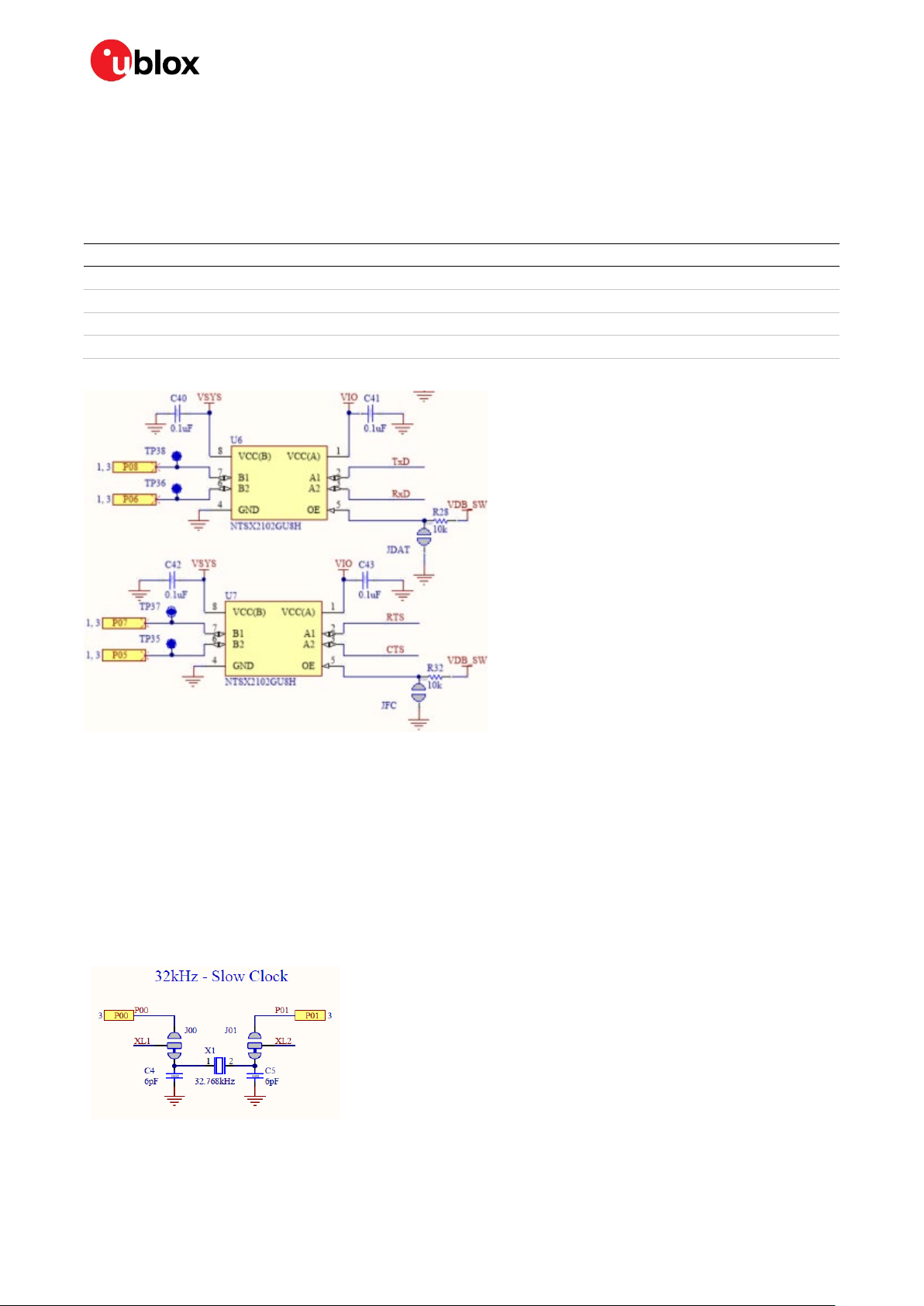
2.5 Virtual COM port
The evaluation board allows for easy serial communication with the BMD-345 module and a connected
computer. The Interface IC provides a virtual COM port USB device that connects to four GPIO pins on
the module, allowing for UART communication with or without hardware flow control. The UART lines
can be isolated from the Interface IC by soldering the associated jumpers.
BMD-345 Pin Name BMD-345 Function Jumper Interface IC Function
P0.05 RTS JFC CTS
P0.06 TXD JDAT RXD
P0.07 CTS JFC RTS
P0.08 RXD JDAT TXD
Table 2: Virtual COM port connections
Figure 7: Interface IC UART circuit
2.6 32 kHz crystal oscillator
The evaluation board has a 32.768 kHz crystal oscillator connected to the BMD-345 module by
default. This allows the module to use any of the three available low frequency (LF) clock sources: an
internal calibrated RC oscillator, an internal synthesized clock (derived from the 32 MHz clock), or an
external crystal oscillator. The external crystal oscillator is the most accurate and lowest power LF
clock option. For applications without strict time keeping requirements, the internal calibrated RC
oscillator is often suitable. The crystal is connected to the module through a solder select jumper,
allowing either the crystal or the IO header to be connected to the module’s GPIO pins.
Figure 8: Schematic – 32 kHz crystal
UBX-19051533 - R03 Hardware description Page 10 of 28
C1-Public
Page 11

EVK BMD-345 - User guide
2.7 NFC connector
Connection to an external NFC antenna is provided through a Molex flat-flex connector, Part number
051281-0594. Capacitors “C2” and “C3” provide tuning of the NFC antenna for resonance at 15.56
MHz.
Figure 9: NFC connector
2.8 Current sensing headers
The evaluation board provides two current sensing headers. “JBMD” allows for power consumption
measurement of the BMD-345 module and “JSHD” allows for power consumption measurement of
the shields connected to the Arduino-style headers (“VSHLD” power only).
Each 3-pin 2.54 mm pitch header has two pins connected across a 1 Ω current-sense resistor
powering the module or the shield, and the third pin to ground. To measure current consumption, use
a multimeter or other precision voltage measurement device to measure voltage drop across pins one
and two. Current can also be measured directly by removing “RBMD” / “RSHD” and using a current
meter in series with the two voltage pins. The default hardware configuration does not require any
modification of the current sense headers for the BMD-345-EVAL to perform properly.
☞ Only current flowing through “VBMD” into the module is measured; current flowing into GPIO pins
is not measured.
Figure 10: Current sensing header layout
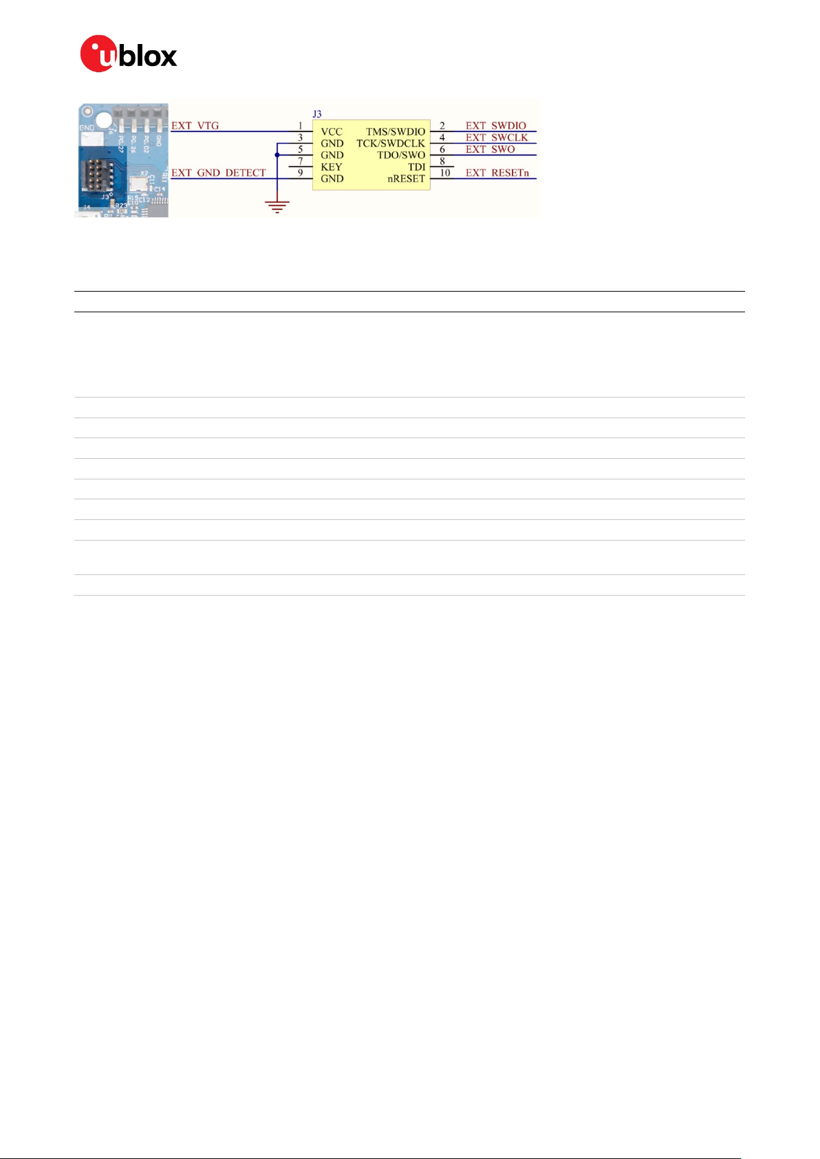
2.9 External SEGGER J-Link™ debug interface
External target hardware, for example ANNA-B1, NINA-B1/B3, and BMD modules, can be connected
to J3 for firmware programming and debug. The SEGGER J-LINK-OB debug interface is implemented
as shown in Figure 11. J3 is implemented with a 2x5, 10-pin header on 1.27 mm centers.
UBX-19051533 - R03 Hardware description Page 11 of 28
C1-Public
Page 12
EVK BMD-345 - User guide
the use of an external SEGGER J-Link Debug Probe.
Figure 11: External J-Link debug interface
In order to enable the external J-Link connection, ensure the following are implemented on the target
hardware:
Pin Number Signal Type Description
1 EXT_VTG I Connect EXT_VTG to the module power supply (VCC) on the target
hardware. Used by the debug interface as an input to sense power applied
to the external circuit. Only voltages of 3.0 V to 3.3 V are supported.
☞ Target hardware VCC operating voltages outside 3.0 V to 3.3 V require
2 EXT_SWDIO I/O
3 GND Power Connect to SWDIO on the target hardware
4 EXT_SWDCLK O
5 GND Power Connect to SWDIO on the target hardware
6 EXT_SWO I Connect to SWO on the target hardware (optional)
7 N/C Not connected (key)
8 N/C Not connected
9 EXT_GND_DETECT I Connect EXT_GND_DETECT to GND on the target hardware. Used by the
debug interface to detect the presence of external target hardware.
10 EXT_RESET_N I/O Connect to RESET_N on the target hardware (optional)
Table 3: J3 debug connector pin-out
☞ At this point, the debug interface will interact with the target hardware instead of the on-board
BMD-345 module.
UBX-19051533 - R03 Hardware description Page 12 of 28
C1-Public
Page 13

EVK BMD-345 - User guide
2.10 QSPI
A 64 Mbit Quad SPI (MX25R6435F) flash is available on the BMD-345-EVAL. This memory can be used
for execute in place (XIP) directly from the flash as well as general data storage.
Figure 12: Quad SPI flash
2.11 GPIO jumpers
Many solder bridge jumpers on the board are available to allow GPIO configuration. Most solder
jumpers are used to remove on-board components from the module’s GPIO nets to eliminate
interference with external circuitry added on the I/O headers. All GPIOs are directly connected to the
I/O Headers by default, except P0.00 & P0.01 (32 kHz crystal), P0.09 & P0.10 (NFC antenna), and
P0.17 & P0.20 - P0.23 (QSPI). These are disconnected from the I/O headers as they would interfere
with the default functions. The GPIO jumpers are shown on the bottom of the BMD-345 evaluation kit
PCB.
Figure 13: GPIO jumpers
UBX-19051533 - R03 Hardware description Page 13 of 28
C1-Public
Page 14

EVK BMD-345 - User guide
2.12 Header pin-out
Headers J5 - J9 and J11 break out the IO signals from the BMD-345 module on 2.54 mm pitch
headers.
Figure 14: EVK BMD-345 evaluation board (top view)
⚠ The I/O pins of the BMD-345 EVK are not 5 V tolerant. Arduino Uno® style shields shall be
configured to use +3.3 V DC (VSHLD) as the I/O voltage reference.
The tables below are presented in order of the headers on the BMD-345-Eval board.
Pin Pin name nRF52840 Function
1 VSHLD - +3.3 V Shield Power
2 VSHLD - +3.3 V Shield Power
3 RESET P0.18 RESET_N / GPIO
4 VSHLD - +3.3 V Shield Power
5 5V0 - +5.0 V USB Power
6 GND - Ground
7 GND - Ground
8 - - No connection
Table 4: Header J5
UBX-19051533 - R03 Hardware description Page 14 of 28
C1-Public
Page 15

EVK BMD-345 - User guide
Pin Pin name nRF52840 Function
1 P0.27 P0.27 GPIO
2 P0.26 P0.26 GPIO
3 P0.02 P0.02 GPIO / AIN0
4 GND - Ground
5 P1.15 P1.15 GPIO
6 P1.14 P1.14 GPIO
7 P1.13 P1.13 GPIO
8 P1.12 P1.12 GPIO
9 P1.11 P1.11 GPIO
10 P1.10 P1.10 GPIO
Table 5: Header J6
Pin Pin name nRF52840 Function
1 P1.08 P1.08 GPIO
2 P1.07 P1.07 GPIO
3 - - No connection
4 - - No connection
5 - - No connection
6 P1.03 P1.03 GPIO
7 - - No connection
8 P1.01 P1.01 GPIO
Table 6: Header J7
Pin Pin name nRF52840 Function
1 P0.03 P0.03 GPIO / AIN1
2 P0.04 P0.04 GPIO / AIN2
3 P0.28 P0.28 GPIO / AIN4
4 P0.29 P0.29 GPIO / AIN5
5 P0.30 P0.30 GPIO / AIN6
6 P0.31 P0.31 GPIO / AIN7
Table 7: Header J8
Pin Pin name nRF52840 Function
1 P0.10 P0.10 OPEN / GPIO
2 P0.09 P0.09 OPEN / GPIO
3 P0.08 P0.08 GPIO
4 P0.07 P0.07 GPIO / TRACECLK
5 P0.06 P0.06 GPIO
6 P0.05 P0.05 GPIO / AIN3
7 P0.01 P0.01 OPEN / GPIO
8 P0.00 P0.00 OPEN / GPIO
Table 8: Header J9
UBX-19051533 - R03 Hardware description Page 15 of 28
C1-Public
Page 16

EVK BMD-345 - User guide
Pin Pin name nRF52840 Function
1 P0.11 P0.11 GPIO / TRACED[2]
2 P0.12 P0.12 GPIO / TRACED[1]
3 P0.13 P0.13 GPIO
4 P0.14 P0.14 GPIO
5 P0.15 P0.15 GPIO
6 P0.16 P0.16 GPIO
7 P0.17 P0.17 OPEN / GPIO / QSPI CS
8 P0.18 P0.18 RESET_N / GPIO
9 P0.19 P0.19 OPEN / GPIO / QSPI CLK
10 P0.20 P0.20 OPEN / GPIO / QSPI DIO0
11 P0.21 P0.21 OPEN / GPIO / QSPI DIO1
12 P0.22 P0.22 OPEN / GPIO / QSPI DIO2
13 P0.23 P0.23 OPEN / GPIO / QSPI DIO3
14 P0.24 P0.24 GPIO
15 P0.25 P0.25 GPIO
16 P1.00 P1.00 GPIO / TRACED[0] / SWO
17 P1.09 P1.09 OPEN / GPIO / TRACED[3]
18 - - No connection
Table 9: Header J10
Pin Pin name nRF52840 Function
1 P1.14 P1.14 GPIO
2 5V0 - +5.0 V USB Power
3 P1.15 P1.15 GPIO
4 P1.13 P1.13 GPIO
5 RESET P0.18 RESET_N / GPIO
6 GND Ground
Table 10: Header J11
UBX-19051533 - R03 Hardware description Page 16 of 28
C1-Public
Page 17

EVK BMD-345 - User guide
3 Setting up the evaluation board
This section provides information on how to set up and program the BMD-345 evaluation kit with an
example application.
3.1 Set up the tool chain
1. Install SEGGER Embedded Studio and request a license.
1.1. Training videos for SEGGER Embedded Studio can be viewed here.
2. Download the latest nRF5 SDK. Unzip it to a convenient working directory. The latest SDK version
should be used whenever possible. The “nRF5_SDK_xx.x.x_yyyyyyy” directory may change. The
folders under usually remain the same from version to version.
☞ Do not alter the directory trees. The examples are configured for relative path positions.
☞ Do not use spaces in the directory path.
3. When selecting examples from the SDK, note the following cross reference:
u-blox evaluation board Nordic SoC Preferred Nordic SoftDevice Compatible Nordic DK
BMD-345-EVAL nRF52840 S140 PCA10056 / nRF52840 DK
Table 11: u-blox evaluation with Nordic DK cross reference
4. Install nRF Connect for desktop and optionally one of the mobile versions. nRF Connect can be
used directly with the Device Under Test (DUT) evaluation board for programming and other
features.
5. Install the mobile nRF Blinky for Android or nRF Blinky for iOS. nRF Blinky will be used later in
this guide.
☞ If using nRF Connect on a desktop, a second evaluation board or an nRF52 USB Dongle is required
to make Bluetooth low energy connections with your DUT.
6. Install the SEGGER J-Link Commander. If presented with a screen to select different IDEs,
ensure at least the “SEGGER Embedded Studio ARM” line is selected:
Figure 15: SEGGER J-Link commander install
7. You may need to add the install location to the system PATH. The default location for the
J-Link commander is “
number.
8. Install nRF Toolbox for your mobile device. This will be used with the example below.
UBX-19051533 - R03 Setting up the evaluation board Page 17 of 28
C1-Public
C:\Program Files (x86)\SEGGER\JLink_Vnnn” where “nnn” is the version
Page 18

EVK BMD-345 - User guide
3.2 Connect BMD-345 evaluation kit to a computer
The evaluation board is provided with an on-board SEGGER J-Link programmer/debugger.
1. Connect one of the 2.4GHz antennas from the kit to the module.
⚠ Note that the U.FL connector is intended for limited connect / disconnect cycles.
2. Connect the board to a computer using the USB cable provided.
☞ The status LED, D5, will flash and then turn solid once the USB device is enumerated. Some
flickering is normal.
3. After a few seconds, the computer will recognize the evaluation board as a J-Link device and
install the USB-Virtual COM Port device driver.
4. Run the J-Link Commander:
4.1. JLink on Windows
4.2. JLinkExe on macOS and Linux
☞ If prompted to update the J-Link firmware, accept and perform the update.
5. Type “connect” at the J-Link> prompt
6. Enter the device type at the Device> prompt
6.1. Type nRF52840_XXAA for the BMD-345
7. Enter S to select the SWD interface and accept the default for the speed.
8. J-Link will respond with several items. Here is a sample output:
UBX-19051533 - R03 Setting up the evaluation board Page 18 of 28
C1-Public
Page 19

EVK BMD-345 - User guide
Figure 16: J-Link commander output
9. This confirms that the evaluation board is properly recognized.
10. While still in the J-Link Commander session, save the pre-programmed public Bluetooth address
by typing in: savebin mac_addr.bin 0x10001080 8
11. Save the file mac_addr.bin to a convenient location for future use.
12. Exit the J-Link session by typing exit.
At this point, a file titled mac_addr.bin will be saved in the current directory. The contents will
contain the MAC address in little-endian format:
33 22 11 93 54 94 FF FF
to correspond to the address 94:54:93:11:22:33. The last two FF values are only fillers to complete
the 8-byte read. Public Bluetooth addresses begin with the IEEE-assigned company ID, 94:54:93 or
6C:1D:EB. The remaining bytes are printed on the 2D and human-readable label on the module. See
the module data sheet for additional information.
☞ This file may be used to restore the Bluetooth address after performing an erase or recover with
the J-Link command: loadbin mac_address.bin 0x10001080
UBX-19051533 - R03 Setting up the evaluation board Page 19 of 28
C1-Public
Page 20

EVK BMD-345 - User guide
3.3 Modify an example to enable the PA / LNA
The BMD-345 incorporates both the Nordic Semiconductor nRF52840 SoC and Skyworks RFX2411
RF front end (PA / LNA). The front end must be configured in order for the module to function properly.
This guide shows an example of the dynamic control using the S140 SoftDevice. Other types of
control are discussed in the BMD-345 data sheet.
3.3.1 Example setup
It’s good practice to create a copy of an SDK example so the original code is not modified. For the
example here, start with the ble_app_blinky example:
C:\u-blox\nRF5_SDK_16.0.0_98a08e2\examples\ble_peripheral\ble_app_blinky
Copy the entire folder structure to a new folder in the same example folder, for example:
C:\u-blox\nRF5_SDK_16.0.0_98a08e2\examples\ble_peripheral\ble_app_blinky_sd
Add a file called custom_board.h. This is used to define the required GPIO. It’s easiest to start with the
existing nRF52840 DK configuration file, pca10056.h, which is located here:
C:\u-blox\nRF5_SDK_16.0.0_98a08e2\components\boards\pca10056.h
Copy and rename it to:
C:\u-blox\nRF5_SDK_16.0.0_98a08e2\examples\ble_peripheral\ble_app_blinky_sd\pca10056\s140
\config\custom_board.h
Open the copied example in SEGGER Embedded Studio (SES):
C:\u-blox\nRF5_SDK_16.0.0_98a08e2\examples\ble_peripheral\ble_app_blinky_sd\pca10056\s140
\ses\ble_app_blinky_pca10056_s140.emProject
Right-click on the “Application” folder.
Select “Add existing file”. Navigate to the custom_board.h file. The project should now look like this:
Figure 17: Add custom_board.h to project
UBX-19051533 - R03 Setting up the evaluation board Page 20 of 28
C1-Public
Page 21

EVK BMD-345 - User guide
Right-click on the project (Project ‘ble_app_blinky_pca10056_s140”) and select Options. The
following window will appear:
Figure 18: Project options
Click on “Preprocessor”, then select “Common” from the drop-down:
Figure 19: Preprocessor common options
Double-click on the “Preprocessor Definitions” to show the list. Change “BOARD_PCA10056” to
“BOARD_CUSTOM”. This directs the IDE to reference the custom_board.h file that was just added:
UBX-19051533 - R03 Setting up the evaluation board Page 21 of 28
C1-Public
Page 22

EVK BMD-345 - User guide
Figure 20: Change to BOARD_CUSTOM
Click OK on the Preprocessor Definitions and Options windows to close them.
Open custom_board.h and add the following lines:
// Pins required for BMD-345 PA / LNA
#define PA_RX_EN_PIN NRF_GPIO_PIN_MAP(1,6)
#define PA_TX_EN_PIN NRF_GPIO_PIN_MAP(1,5)
#define PA_MODE_PIN NRF_GPIO_PIN_MAP(1,4)
#define PA_A_SEL_PIN NRF_GPIO_PIN_MAP(1,2)
Any other custom pin definitions may be added in custom_board.h.
A small block of code needs to be added to the application to enable this feature. In main.c, add the
following function above the advertising_start() function:
static void pa_lna_assist(uint32_t gpio_pa_pin, uint32_t gpio_lna_pin)
{
ret_code_t err_code;
static const uint32_t gpio_toggle_ch = 0;
static const uint32_t ppi_set_ch = 0;
static const uint32_t ppi_clr_ch = 1;
// Configure SoftDevice PA / LNA assist
ble_opt_t opt;
memset(&opt, 0, sizeof(ble_opt_t));
// Common PA / LNA config
// GPIOTE channel
opt.common_opt.pa_lna.gpiote_ch_id = gpio_toggle_ch;
// PPI channel for pin learing
opt.common_opt.pa_lna.ppi_ch_id_clr = ppi_clr_ch;
// PPI channel for pin setting
opt.common_opt.pa_lna.ppi_ch_id_set = ppi_set_ch;
UBX-19051533 - R03 Setting up the evaluation board Page 22 of 28
C1-Public
Page 23

EVK BMD-345 - User guide
// PA config
// Set the pin to be active high
opt.common_opt.pa_lna.pa_cfg.active_high = 1;
// Enable toggling
opt.common_opt.pa_lna.pa_cfg.enable = 1;
// The GPIO pin to toggle
opt.common_opt.pa_lna.pa_cfg.gpio_pin = gpio_pa_pin;
// LNA config
// Set the pin to be active high
opt.common_opt.pa_lna.lna_cfg.active_high = 1;
// Enable toggling
opt.common_opt.pa_lna.lna_cfg.enable = 1;
// The GPIO pin to toggle
opt.common_opt.pa_lna.lna_cfg.gpio_pin = gpio_lna_pin;
err_code = sd_ble_opt_set(BLE_COMMON_OPT_PA_LNA, &opt);
APP_ERROR_CHECK(err_code);
}
Modify the advertising_start() function to include control configuration:
static void advertising_start(void)
{
ret_code_t err_code;
//Insert the following code before calling scan_start() or advertising_start ()
/*------------------------------------------------------------------------*/
//Set PA / LNA Mode Pin: Low for Normal operation
nrf_gpio_cfg_output(PA_MODE_PIN);
nrf_gpio_pin_clear(PA_MODE_PIN);
//Set PA / LNA Select Pin: low for U.FL
nrf_gpio_cfg_output(PA_A_SEL_PIN);
nrf_gpio_pin_clear(PA_A_SEL_PIN);
//Setup PA / LNA TX and RX control pins with the SoftDevice
pa_lna_assist(PA_TX_EN_PIN,PA_RX_EN_PIN);
//Set TX power for scan responses
sd_ble_gap_tx_power_set(BLE_GAP_TX_POWER_ROLE_SCAN_INIT, 0,
RADIO_TXPOWER_TXPOWER_Neg20dBm);
//Set TX power for advertisements
sd_ble_gap_tx_power_set(BLE_GAP_TX_POWER_ROLE_ADV, 0,
RADIO_TXPOWER_TXPOWER_Neg20dBm);
//Tx power setting for connections inherit the scan or advertising power setting
/*-------------------------------------------------------------------------*/
err_code = sd_ble_gap_adv_start(m_adv_handle, APP_BLE_CONN_CFG_TAG);
APP_ERROR_CHECK(err_code);
bsp_board_led_on(ADVERTISING_LED);
}
3.3.2 Example test
Click the “build” icon or press <F7> to compile the example and ensure there are no errors.
Download the example to the BMD-345-Eval board, then press the RESET button on the board. The
BMD-345 will illuminate LED1 and start advertising “Nordic_Blinky”.
A logic analyzer or oscilloscope may be used to observe the control signals. Test points are located
near the BMD-345:
UBX-19051533 - R03 Setting up the evaluation board Page 23 of 28
C1-Public
Page 24

EVK BMD-345 - User guide
Figure 21: RF front end control test points
Figure 22: Control signals on logic analyzer
Open the “nRF Blinky” mobile application. Connect to the “Nordic_Blinky” device:
Figure 23: nRF Blinky scanning for devices
LED1 will go off, and LED2 will illuminate.
Operate the functions. Tap the slider to toggle LED3, and press Button 1 on the BMD-345-Eval to
change the state reported in the app:
UBX-19051533 - R03 Setting up the evaluation board Page 24 of 28
C1-Public
Page 25

EVK BMD-345 - User guide
Figure 24: nRF Blinky interaction with BMD-345-Eval
nRF Connect can also be used to observe the RSSI and operate the example with manual interaction
with the Bluetooth characteristics.
Figure 25: nRF Connect interaction with BMD-345-Eval
UBX-19051533 - R03 Setting up the evaluation board Page 25 of 28
C1-Public
Page 26

EVK BMD-345 - User guide
Related documents
[1] BMD-345 data sheet, UBX-19039908
[2] Skyworks RFX2411 data sheet
[3] Nordic nRF52840 product specification
[4] S140 SoftDevice specification
[5] u-blox package information guide, UBX-14001652
☞ For product change notifications and regular updates of u-blox documentation, register on our
website, www.u-blox.com.
UBX-19051533 - R03 Related documents Page 26 of 28
C1-Public
Page 27

EVK BMD-345 - User guide
Revision history
Revision Date Comments
R01 05-Dec-2019 Initial release.
R02 17-Feb-2021 Updated renderings to photos of actual EVK.
R03 16-Apr-2021 Updated Figure 14
UBX-19051533 - R03 Revision history Page 27 of 28
C1-Public
Page 28

EVK BMD-345 - User guide
Contact
For complete contact information, visit us at www.u-blox.com.
u-blox Offices
North, Central and South America
u-blox America, Inc.
Phone: +1 703 483 3180
E-mail: info_us@u-blox.com
Regional Office West Coast:
Phone: +1 408 573 3640
E-mail: info_us@u-blox.com
Technical Support:
Phone: +1 703 483 3185
E-mail: support@u-blox.com
Headquarters
Europe, Middle East, Africa
u-blox AG
Phone: +41 44 722 74 44
E-mail: info@u-blox.com
Support: support@u-blox.com
Asia, Australia, Pacific
u-blox Singapore Pte. Ltd.
Phone: +65 6734 3811
E-mail: info_ap@u-blox.com
Support: support_ap@u-blox.com
Regional Office Australia:
Phone: +61 3 9566 7255
E-mail: info_anz@u-blox.com
Support: support_ap@u-blox.com
Regional Office China (Beijing):
Phone: +86 10 68 133 545
E-mail: info_cn@u-blox.com
Support: support_cn@u-blox.com
Regional Office China (Chongqing):
Phone: +86 23 6815 1588
E-mail: info_cn@u-blox.com
Support: support_cn@u-blox.com
Regional Office China (Shanghai):
Phone: +86 21 6090 4832
E-mail: info_cn@u-blox.com
Support: support_cn@u-blox.com
Regional Office China (Shenzhen):
Phone: +86 755 8627 1083
E-mail: info_cn@u-blox.com
Support: support_cn@u-blox.com
Regional Office India:
Phone: +91 80 405 092 00
E-mail: info_in@u-blox.com
Support: support_in@u-blox.com
Regional Office Japan (Osaka):
Phone: +81 6 6941 3660
E-mail:
Support: support_jp@u-blox.com
Regional Office Japan (Tokyo):
Phone: +81 3 5775 3850
E-mail: info_jp@u-blox.com
Support: support_jp@u-blox.com
Regional Office Korea:
Phone: +82 2 542 0861
E-mail: info_kr@u-blox.com
Support: support_kr@u-blox.com
Regional Office Taiwan:
Phone: +886 2 2657 1090
E-mail: info_tw@u-blox.com
Support: support_tw@u-blox.com
info_jp@u-blox.com
UBX-19051533 - R03 Contact Page 28 of 28
C1-Public
 Loading...