

Page 1
UBX-17015029 - R06
C1-Public www.u-blox.com
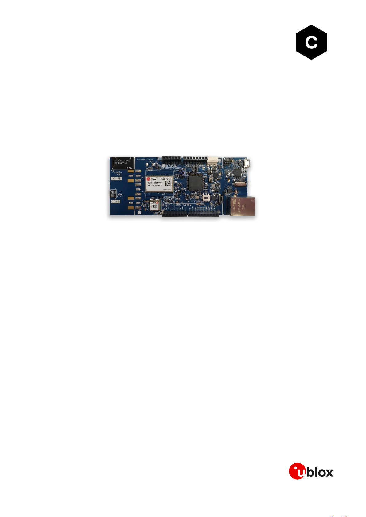
C030
LTE Cat 1, Cat M1, NB-IoT and 2G/3G mbed-enabled IoT
starter kit
User guide
Abstract
This guide explains how to set up the C030 Arm® Mbed Enabled™ Internet of Things Starter Kit to
begin evaluating u-blox 2G/3G/4G cellular and GNSS modules.
+
Page 2
C030 - User guide
UBX-17015029 - R06 Document information Page 2 of 34
C1-Public
Document information
Title
C030
Subtitle
LTE Cat 1, Cat M1, NB-IoT and 2G/3G mbed-enabled IoT starter kit
Document type
User guide
Document number
UBX-17015029
Revision and date
R06
03-Feb-2021
Disclosure restriction
C1-Public
Product status
Corresponding content status
Functional sample
Draft
For functional testing. Revised and supplementary data will be published later.
In development /
Prototype
Objective Specification
Target values. Revised and supplementary data will be published later.
Engineering sample
Advance Information
Data based on early testing. Revised and supplementary data will be published later.
Initial production
Early Production Information
Data from product verification. Revised and supplementary data may be published later.
Mass production /
End of life
Production Information
Document contains the final product specification.
This document applies to the following products:
Product name
Type number
Firmware version
PCN reference
Product status
C030
C030-U201-0-00
G0.V.00.00.10R
UBX-18007786
Initial production
C030-N211-0-00
G0.V.00.00.10R
UBX-18007786
Obsolete
C030-R410M-0-00
N.A.
UBX-18047677
Obsolete
C030-R3121-0-00
N.A.
UBX-18047677
Obsolete
u-blox or third parties may hold intellectual property rights in the products, names, logos and designs included in this
document. Copying, reproduction, modification or disclosure to third parties of this document or any part thereof is only
permitted with the express written permission of u-blox.
The information contained herein is provided “as is” and u-blox assumes no liability for its use. No warranty, either express or
implied, is given, including but not limited to, with respect to the accuracy, correctness, reliability and fitness for a particular
purpose of the information. This document may be revised by u-blox at any time without notice. For the most recent
documents, visit www.u-blox.com.
Arduino® is a trademark of Arduino Srl or Arduino LLC registered and/or used in the EU, the U.S. and other countries/regions.
Arm and Mbed™ are registered trademarks of Arm Limited (or its subsidiaries) in the US and/or elsewhere.
JT® is a registered trademark of JTGlobal Limited in the EU, the U.S. and other countries/regions
Copyright © u-blox AG.
Page 3

C030 - User guide
UBX-17015029 - R06 Contents Page 3 of 34
C1-Public
Contents
Document information ................................................................................................................................ 2
Contents .......................................................................................................................................................... 3
1 Overview ................................................................................................................................................... 4
Using this guide .................................................................................................................................................... 4
Warnings and certifications .............................................................................................................................. 5
2 Hardware description ........................................................................................................................... 6
2.1 C030 block diagram .................................................................................................................................... 9
2.2 Buttons, jumpers and switches ............................................................................................................. 16
2.2.1 Utilization of cellular modem USB sniffer (and programmer) .................................................. 17
2.3 LED indicators ........................................................................................................................................... 18
2.4 Connectors ................................................................................................................................................. 19
2.5 Configuration links / components ......................................................................................................... 20
2.6 Test, break out points, and debug interfaces ..................................................................................... 24
2.7 Arduino™ UNO R3 compatible interface pin out ................................................................................. 25
2.8 Power supply options and LiPo battery usage .................................................................................... 26
2.9 C030-N211 variant cellular module firmware upgrade ...................................................................... 27
3 Getting started .................................................................................................................................... 28
3.1 eUICC (embedded SIM) activation ......................................................................................................... 28
3.2 C030 board setup ..................................................................................................................................... 28
3.3 Development PC USB driver configuration .......................................................................................... 28
3.4 Getting started with Mbed ...................................................................................................................... 29
4 Approvals ............................................................................................................................................... 30
4.1 C030-U201 European Conformance CE mark .....................................................................................30
4.2 C030-N211 European Conformance CE mark ...................................................................................... 31
Appendix ....................................................................................................................................................... 32
A Glossary ................................................................................................................................................. 32
Related documentation ........................................................................................................................... 33
Revision history .......................................................................................................................................... 33
Contact .......................................................................................................................................................... 34
Page 4

C030 - User guide
UBX-17015029 - R06 Overview Page 4 of 34
C1-Public
1 Overview
The u-blox C030 LTE Cat 1, Cat M1, NB-IoT and 2G/3G mbed-enabled IoT starter kit is a versatile
development platform that allows quick prototyping of a variety of applications for low-power Internet
of Things (IoT) devices.
The u-blox C030 boards are delivered in several variants based on the type of u-blox cellular module
employed, such as:
• C030-U201: SARA-U201 HSPA module with 2G fallback
• C030-N211: SARA-N211 NB-IoT (LTE Cat NB1) module
• C030-R410M: SARA-R410M LTE Cat M1 / Cat NB1 module
• C030-R3121: LARA-R3121 LTE Cat 1 single-mode module with GNSS receiver
The u-blox C030 application boards, except C030-R3121, have a u-blox MAX-M8C module or a ZOE
GNSS IC as a concurrent GNSS receiver, thereby enabling straight forward development of locationaware, globally communicating applications.
The u-blox C030 board provides access to a variety of hardware interfaces (10/100 Mb/s Ethernet, 22
GPIOs with SPI, I2C, UART, PWM) through the Arduino™ Uno R3 compatible header connector.
An eUICC (embedded SIM) is integrated on the u-blox C030-U201 / C030-R3121 variants. The eUICC
comes with International Data Roaming Cellular Connectivity Service by JT® JTGlobal (formerly
Jersey Telecom) with 50 MB of data for the period of 90 days, which can be topped up and extended
on demand.
The u-blox C030 board is powered by an Arm® Cortex-M4 based ST® STM32F437VGT Host
microcontroller, which is fully supported by the Arm® Mbed™ platform. The microcontroller has 512 kB
flash, 64 kB RAM, and runs an up-to-96 MHz system clock. The board provides simple USB drag-ndrop programming and ST-Link debug interface for the Host microcontroller. The Arm Mbed platform
provides free software libraries and online tools for professional rapid prototyping. The programming
is done using a standard-based C/C++ SDK. The Arm Mbed compiler also supports full export to
various tool chains, for projects that demand it as they go into production.
The u-blox C030 also works with wide choice of Integrated Development Environments (IDEs)
including but not limited to Arm® Keil®, GCC-based Eclipse IDEs.
Using this guide
This guide assumes the user has basic computer skills and is familiar with the Windows Graphical
User Interface (GUI) and cellular modem environments.
The following symbols are used to highlight important information in the document:
☞ An index finger points out key information pertaining to device operation and performance.
⚠ A warning symbol indicates actions that could negatively impact or damage the device.
Page 5
C030 - User guide
UBX-17015029 - R06 Overview Page 5 of 34
C1-Public
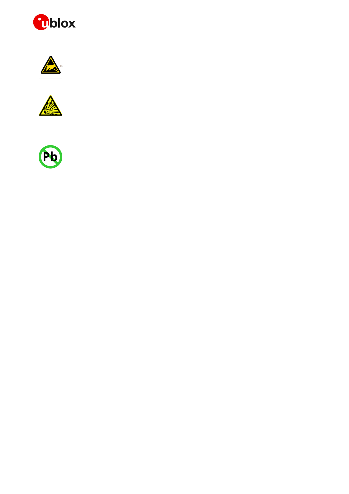
Warnings and certifications
C030 is an Electrostatic Sensitive Device (ESD).
CAUTION! Risk of short circuit of the battery when touching it with conducting
parts. In the unlikely event of a failure in the internal protection circuitry, there is
a risk of an explosion when charging fully or partially discharged batteries.
Replace the battery if it no longer has sufficient charge for unit operation. Control
the battery before using it if the device has not been operated for an extended
period of time.
Products marked with this lead-free symbol on the product label comply with the
“Directive 2002/95/EC of the European Parliament and the Council on the
Restriction of Use of certain Hazardous Substances in Electrical and Electronic
Equipment” (RoHS).
C030 application boards are RoHS compliant and green (no halogens).
Page 6

C030 - User guide
UBX-17015029 - R06 Hardware description Page 6 of 34
C1-Public
2 Hardware description
The u-blox C030 has the following onboard hardware features:
• u-blox cellular functionality
o On C030-U201 – u-blox SARA-U201 HSPA/GSM module, with eUICC (embedded SIM)
o On C030-N211 – u-blox SARA-N211 LTE Cat NB1 (NB-IoT) module, with MicroSIM socket
o On C030-R410M – u-blox SARA-R410M-02B LTE Cat M1 / NB1 module, with MicroSIM socket
o On C030-R3121 – u-blox LARA-R3121 LTE Cat 1 module, with eUICC (embedded SIM)
• u-blox GNSS functionality
o On C030-U201 – u-blox MAX-M8C LCC module able to utilize concurrent reception of up to
three GNSS systems (GPS / Galileo together with GLONASS or BeiDou)
o On C030-N211 – u-blox MAX-M8C LCC module able to utilize concurrent reception of up to three
GNSS systems (GPS / Galileo together with GLONASS or BeiDou)
o On C030-R410M – u-blox ZOE-M8B SiP module able to utilize concurrent reception of up to
three GNSS systems (GPS / Galileo together with GLONASS or BeiDou)
o On C030-R3121 – GPS receiver integrated in u-blox LARA-R3121 module
• STM32F437VG Cortex-M4 Arm host MCU with 1024 kB Flash, 256 kB SRAM and SWD connector
o 12 MHz crystal oscillator for system clock
o 32.768 kHz crystal oscillator for real-time clock
o 1.8 V operation
• On-board ST-Link/V2-1 debugger/programmer with SWD connector
o ST-Link/V2-1 standalone development and debug capability
o USB re-enumeration; Virtual COM port, mass storage device and debug port
o 5V from ST-Link/V2-1 Debug USB VBUS, 3.3V operation
o (CMSIS-DAP variant of the FW with extended features will be available in the future)
• On-board TI
®
bq24295 single cell LiPo battery charger and TI® bq27441-G1 battery fuel gauge
• Molex
®
SPOX™ 5268-03A LiPo battery connector
o Supports battery types like BAK –LP-503759-IS-3 (battery is not included)
• On-board SiLabs
®
CP2105 USB to dual UART bridge as Serial USB Sniffer
o Alternative to ST-Link/V2-1 virtual COM port when ST-LINK/V2-1 is not used/available
o Alternative to main supply and Debug USB 5V VBUS inputs
o Sniffing serial communication between the host MCU and the cellular module
• RGB User LED, and two push buttons: user and reset
• On-board SiLabs
®
Si7034-A10 humidity and temperature sensor
o Utilized temperature sensor only. Cannot be used for humidity measurements
• SD card socket for file storage
• Integrated NB-IoT and GNSS antennas by Antenova
®
on C030-N211’s snap-off antenna section
• SMA RF connectors for 50 Ohm cellular and GNSS active antennas except on C030-N211
• Integrated eUICC including International Data Roaming Cellular Connectivity by JT
®
JTGlobal with
50 MB of data for the first 90 days (except for C030-N211 / C030-R410M)
• MicroSIM card socket on C030-N211 / C030-R410M
• Extension:
o Arduino™ Uno R3 compatible interface
o 6 analog capable inputs
o 8 PWM capable outputs
o 22 GPIOs
o 1 x SPI
o 1 x I2C
o 1 x UART with HW flow control option (RTS, CTS)
Page 7
C030 - User guide
UBX-17015029 - R06 Hardware description Page 7 of 34
C1-Public
• Flexible board power supply:
o 5 V main supply USB, debug USB, and sniffer USB VBUS inputs
o 2.5 V to 5.5 V Arduino UNO R3 VIN input
o 2.8 V to 4.4 V LiPo battery input
• Support of a wide range of Integrated Development Environments (IDEs), including but not limited
to GCC-based IDEs, Arm Mbed
• Arm Mbed Enabled (see http://mbed.org)
Figure 1: C030-U201 application board overview
Page 8
C030 - User guide
UBX-17015029 - R06 Hardware description Page 8 of 34
C1-Public
Figure 2: C030-N211 application board overview
Figure 3: C030-R410M application board overview
LTE Cat M1 / NB1
Multi-Band
Page 9
C030 - User guide
UBX-17015029 - R06 Hardware description Page 9 of 34
C1-Public
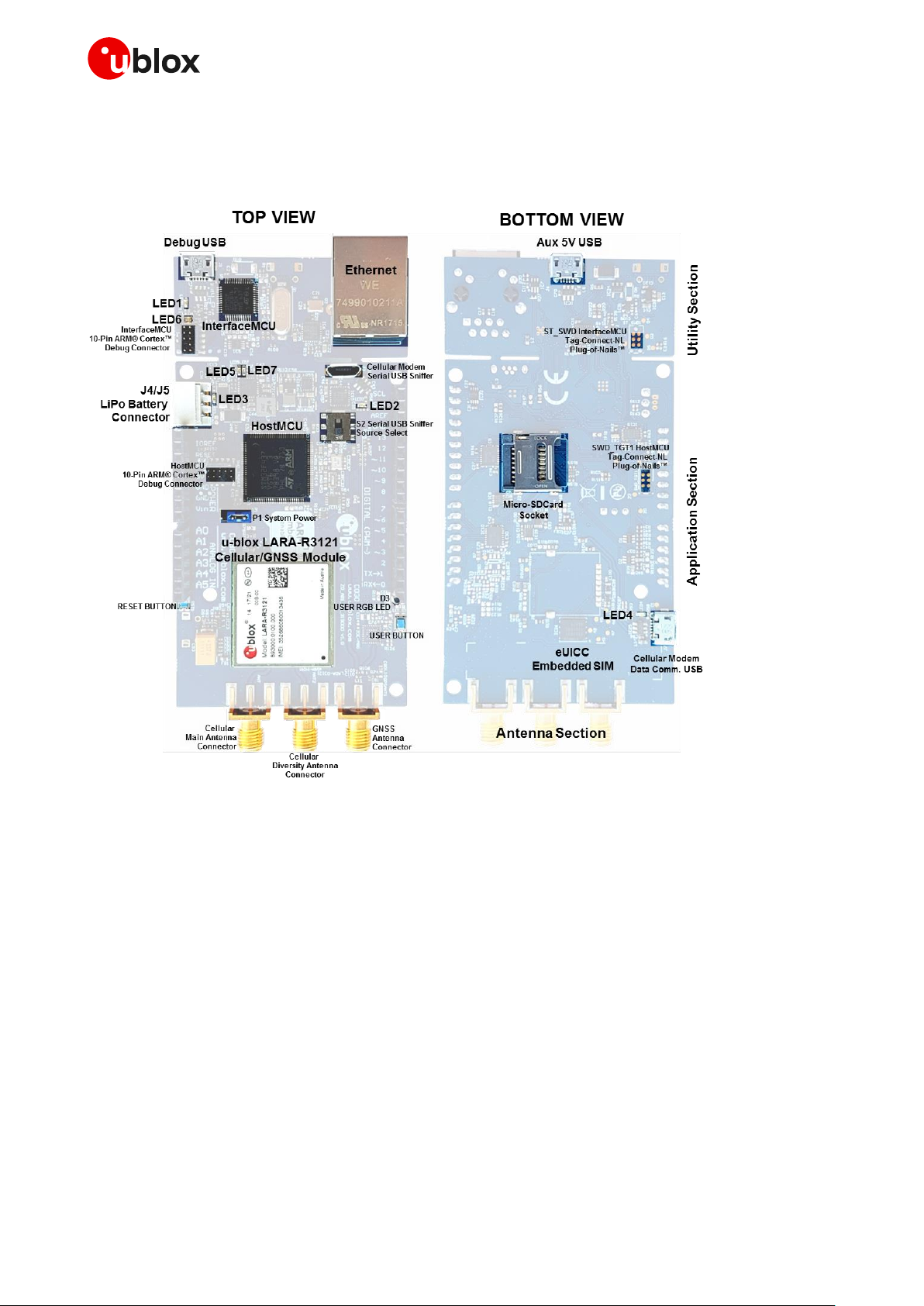
Figure 4: C030-R3121 application board overview
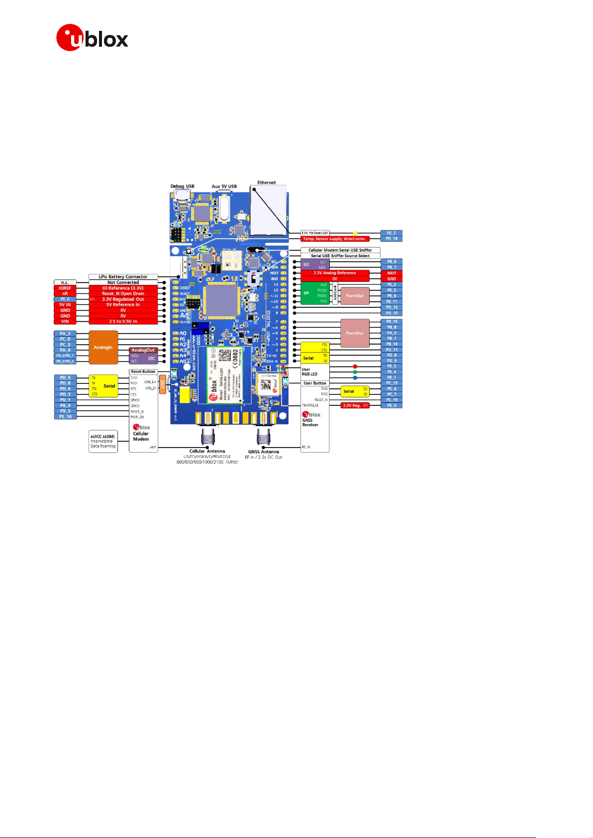
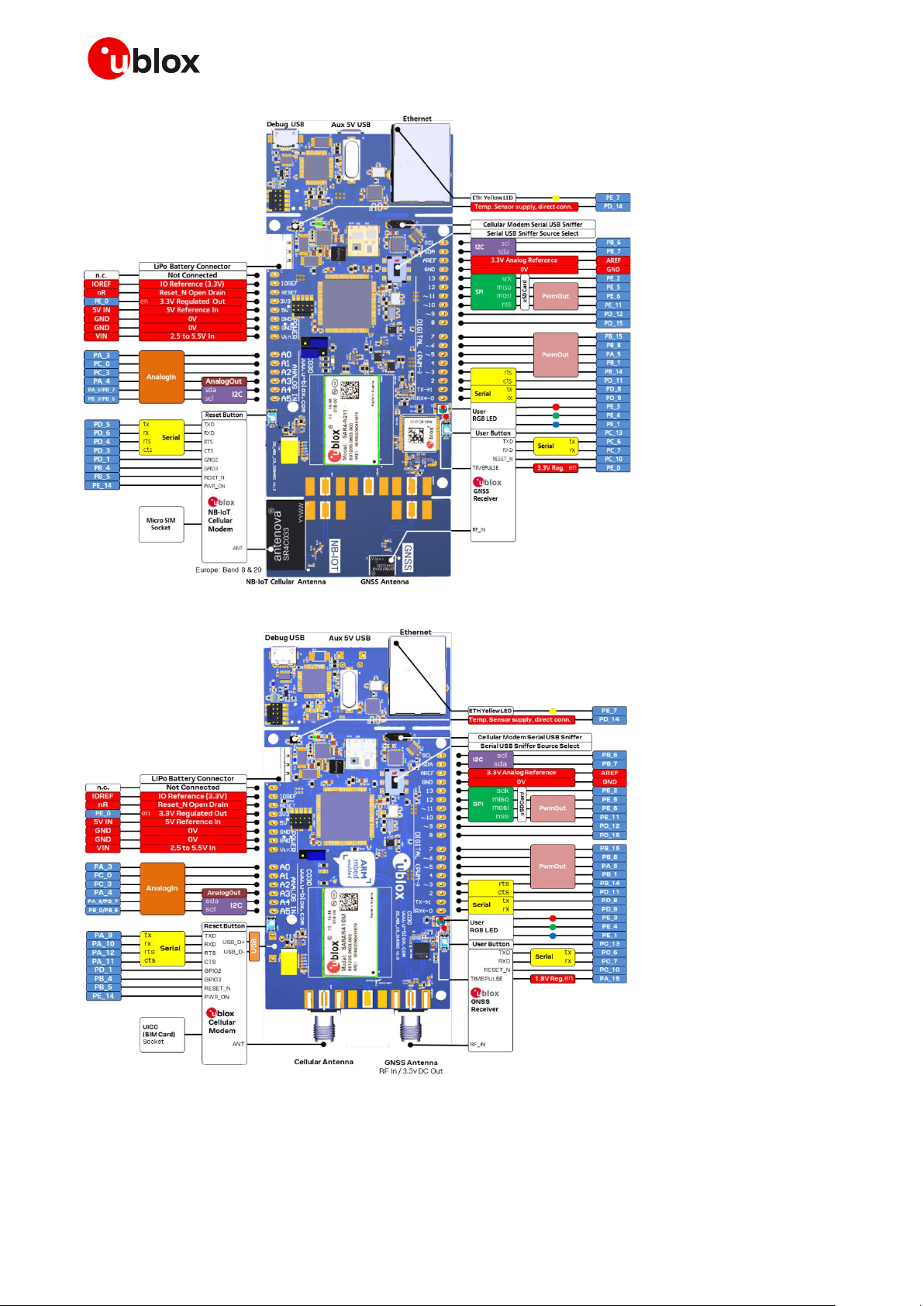
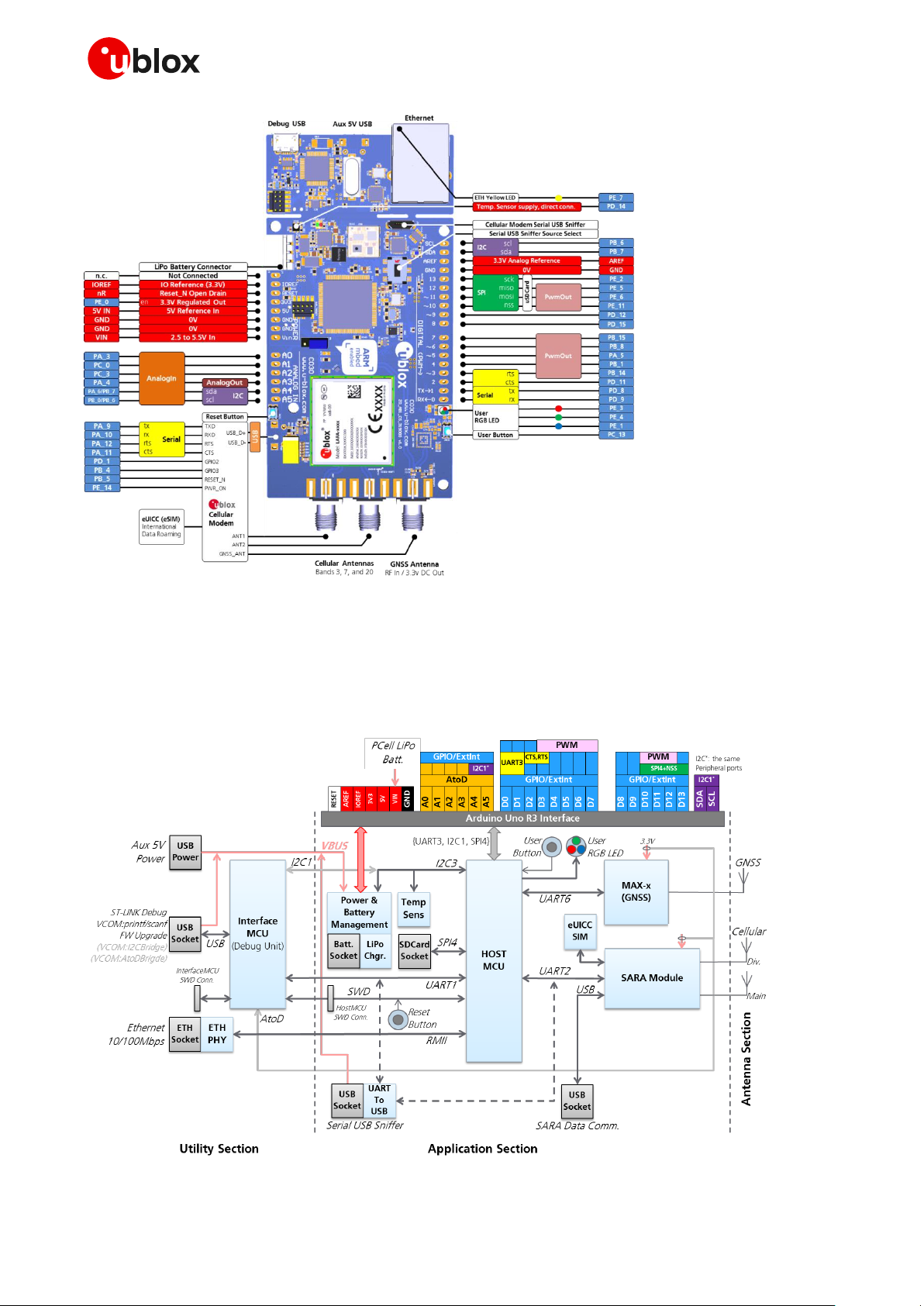
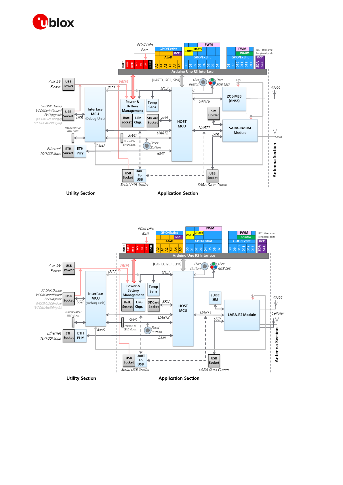
2.1 C030 block diagram
The block diagram of the C030 is depicted in Figure 5, Figure 6 and Figure 7.
Figure 5: C030-U201 / C030-N211 block diagram
VCC
Page 10
C030 - User guide
UBX-17015029 - R06 Hardware description Page 10 of 34
C1-Public
Figure 6: C030-R410M block diagram
Figure 7: C030-R3121 block diagram
Figure 5, Figure 6 and Figure 7 show the major interfaces and internal connections of the C030.
The major component layouts of each board variant are provided in Figure 8, Figure 9, Figure 10 and
Figure 11.
VCC
VCC
Page 11

C030 - User guide
UBX-17015029 - R06 Hardware description Page 11 of 34
C1-Public
The C030 consists of three sections:
• Utility section
The utility section accommodates the components that provide SW debugging / virtual COM port
(ST-Link/CMSIS-DAP) and Ethernet Interface functions. The SW debugging / virtual COM port
functions are executed by the InterfaceMCU via the “Debug USB” interface.
As this section is only needed during the application development and test activities, it could be
physically snapped off from the application section to decrease the size and power consumption.
The utility section is powered up from the “Debug USB” 5V VBus. When the “Debug USB” is not
connected, SW debugging / virtual COM port and Ethernet Interface functions are turned off and
isolated from the Application section.
The “Auxiliary 5V USB” connector on the Utility section could be used to boost the power input to the
application section if the current input from the “Debug USB” 5V Vbus is not sufficient.
• Application section
The application section accommodates the GNSS and cellular modules, a eUICC (Embedded SIM) /
MicroSIM socket, the HostMCU, the battery charging/management and power supply circuitry, the
SD card interface and socket, the Serial USB Sniffer for communication between the HostMCU to the
cellular module and similarly to the InterfaceMCU. The application section also has a temperature
sensor for measuring ambient temperature of the board. Reset and user buttons, configuration
jumpers and User and system status indication LEDs are placed in the application section.
The application section is designed for minimal power consumption. Unutilized circuitries and
sections could be either turned off by software or inhibited electronically.
The Arduino Uno R3 interface on the application section could be used to integrate sensors, actuators
and power/battery supply circuitries as Arduino Shields/expansion daughter PCBs.
The application section could run standalone when the utility and antenna sections are snapped off.
• Antenna section
The C030 PCB has been designed to accommodate GNSS and cellular antennas on-board depending
on the build variant. The C030-N211 antenna section could be snapped off if the orientation of the
C030 is in an enclosure required by the application. Both application and antenna sections have SMA
edge connector footprints. Therefore, by soldering the SMA Edge connectors, the antenna section
can be connected to the application section through adequate 50 Ω RF cables.
The other C030 variants have SMA Jack edge connectors for cellular and GNSS antennas.
Page 12

C030 - User guide
UBX-17015029 - R06 Hardware description Page 12 of 34
C1-Public
Figure 8: C030-U201 major component locations
Page 13

C030 - User guide
UBX-17015029 - R06 Hardware description Page 13 of 34
C1-Public
The C030-N211 NB-IoT variant has a different component and PCB configuration.
• There is no international data roaming eUICC (embedded SIM) on the PCB. Instead, there is a
MicroSIM card socket.
• There is no cellular modem data communication USB connector and relevant circuitry, as
SARA-N2 series modules do not support USB device communication.
• In contrast to C030-U201, the C030-N211 has integrated NB-IoT and GNSS antennas by Antenova
on the antenna section PCB.
The C030-N211 NB-IoT variant specific component locations are shown in Figure 9.
Figure 9: C030-N211 variant specific component locations
Page 14

C030 - User guide
UBX-17015029 - R06 Hardware description Page 14 of 34
C1-Public
The connectors unique to the C030-R410M LTE Cat M1 / NB-IoT variant are:
• There is no international data roaming eUICC (embedded SIM) on the PCB. Instead, there is a
MicroSIM card socket
The C030-R410M LTE Cat M1 / NB-IoT variant specific component locations are shown in Figure 10.
Figure 10: C030-R410M major component locations
Page 15
C030 - User guide
UBX-17015029 - R06 Hardware description Page 15 of 34
C1-Public
The connector specific to the C030-R3121 LTE Cat 1 variant is:
• Diversity cellular antenna connector
The C030-R3121 LTE Cat 1 variant specific component locations are shown in Figure 11.
Figure 11: C030-R3121 major component locations
Page 16
C030 - User guide
UBX-17015029 - R06 Hardware description Page 16 of 34
C1-Public
2.2 Buttons, jumpers and switches
The C030 is equipped with several buttons, jumpers and a switch that the user can easily utilize. The
functions and locations of these components are provided in Table 1 and shown in Figure 8.
Annotation
Function
Description
Section
USER
User button
Push button for application use. Connected to HostMCU GPIO
Port PC13
Application
RST1
Reset button
Push button to reset the HostMCU
Application
P1
System Power Jumper
System power input selection:
• Pin 1-2: On board Power/Battery Management (default
configuration)
• Pin 2-3: VIN pin of Arduino Uno R3 Interface
Application
P3
SARA-N2 FW Flashing Jumper
Power supply jumper used for the C030-N211 FW upgrade only.
Non-functional on other variants.
• Pin 1-2: disabled (default configuration)
• Pin 2-3: flashing enabled
Application
S2
Serial USB Sniffer Source Select
Select the cellular module communication UART channel to sniff:
• On C030-U201 / C030-N211
• Position 1: UART2 communication between HostMCU
and cellular module (default configuration)
• Position 2: C030–N211 only debug log output (921,600 b/s
8N1). Non-functional on other variants.
• On C030-R410M / C030-R3121
• Position 1: Isolation
• Position 2: UART1 communication between HostMCU
and cellular module
Application
Table 1: C030 buttons, jumpers, and switches
The C030 P1 and P3 jumpers and S2 switch positions are depicted in Figure 12 and Figure 13.
Figure 12: C030-U201 / C030-N211 jumper and switches
Figure 13: C030-R410M / C030-R3121 jumper and switches
Page 17

C030 - User guide
UBX-17015029 - R06 Hardware description Page 17 of 34
C1-Public
2.2.1 Utilization of cellular modem USB sniffer (and programmer)
The C030 cellular modem USB sniffer provides two virtual UART COM channels to the connected USB
master (development PC). The cellular module USB sniffer USB VBUS 5VDC rail powers the
application section of the C030. The virtual COM ports are utilized as follows:
C030-U201 / C030-N211 variants:
• Standard COM port as on the development PC: HostMCU USART1 Tx “printf” channel sniffing.
o HostMCU USART1 Tx is also connected to the InterfaceMCU on the utility section
o HostMCU USART1 Rx is connected to InterfaceMCU on the utility section
o Host HostMCU USART1 Rx can be connected to the cellular modem USB sniffer standard COM
port Tx channel via R137 link (see Table 4). In this case, do one of the following:
▪ The utility section should be powered off (disconnect Debug USB)
▪ Snap-off the utility section
▪ Remove R133 link (see Table 4)
• Enhanced COM port as on the development PC. Two operation modes can be selected by using the
S2 switch (see Figure 12):
1. S2 Position 1: HostMCU USART2 to cellular module communication. Allows direct access to
the cellular module. In this case, implement the following steps:
▪ Connect the R151 link(see Table 4)
▪ Remove the R105 link or set the HostMCU PD_5 port as GPIO input to avoid collision
▪ This mode is only used for SARA-N2 FW Flashing/Programming for C030-N211 variant.
The P3 Jumper should be configured accordingly to utilize this function (see Table 1)
2. S2 Position 2: SARA-N2 module debug log output (GPIO1) with 921,600 b/s 8N1 configuration
for the C030-N211 variant only.
C030-R410M / C030-R3121 variants:
• Standard COM port as on the development PC: HostMCU USART2 Tx “printf” channel sniffing.
o HostMCU USART2 Tx is also connected to the InterfaceMCU on the utility section
o HostMCU USART2 Rx is connected to InterfaceMCU on the Utility section
o Host HostMCU USART2 Rx can be connected to the cellular modem USB sniffer standard COM
port Tx channel via R137 link (see Table 4). In this case, do one of the following:
▪ The utility section should be powered off (disconnect Debug USB)
▪ Snap-off the utility section
▪ Remove R133 link (see Table 4)
• Enhanced COM port as on the development PC. Two operation modes can be selected by using the
S2 switch (see Figure 13):
1. S2 Position 1: Isolation
2. S2 Position 2: HostMCU USART1 to cellular module communication. Allows direct access to
the cellular module. In this case, do one the following:
▪ Remove R105 link
▪ set the HostMCU PA_5 Port as GPIO input to avoid collusion
☞ Enhanced COM port Mode 1 direct access to the cellular module allows using development PC
applications like u-blox m-center, to exercise the cellular module AT command interface bypassing
the C030 HostMCU.
☞ On the R410M / R3121 variants, usage of USART1 and USART2 have been swapped as compared
with the U201 / N211 variants.
Page 18
C030 - User guide
UBX-17015029 - R06 Hardware description Page 18 of 34
C1-Public
2.3 LED indicators
The C030 has a few LEDs to indicate the board status for generic application use. Due to the low power
design of C030, if the C030 is not connected to an external power source or is powered from battery
only, all the LEDs except D3 (User RGB LED) and LED_G3 (GNSS Time Pulse LED) are off.
As the D3 and LED_G3 LEDs are controlled by the application, they can be completely turned off to
save power.
The C030 LED indicators are listed in Table 2 and their locations are depicted in Figure 8.
Annotation
Function
Description
Color
LED1
Debug USB VBUS
VBUS 5 V indicator for InterfaceMCU supply
LED2
Serial USB Sniffer VBUS
VBUS 5 V indicator for serial USB sniffer supply
LED3
Aux 5 V USB VBUS
VBUS 5 V indicator for 5 VDC supply input
LED4
Cellular module USB VBUS
VBUS 5 V indicator (not available for the C030-N211)
LED5
Battery charging / man. Input
Battery Charging/Management 5 VDC input supply indicator
LED6
STLink/CMSIS-DAP status
InterfaceMCU Debugging/Flashing status RED/GREEN indicator
LED7
Battery charging status
Battery Charging/Management battery charging status indicator
D3
User RGB LED
HostMCU GPIO driven; PE_3: RED, PE_4: GREEN, PE_1: BLUE (all
negative logic)
LED_G31
GNSS time pulse
GNSS status with 1 s blinks. Managed by HostMCU GPIO PA_15.
0 = off, 1 = on
☞ Not supported by C030-R410M / C030-R3121.
ETH Green2
ETH connection speed
Connection speed indication. On:100 Mb/s, Off:10 Mb/s
ETH Yellow2
ETH transaction/traffic
Indicates Ethernet transaction. Controlled by HostMCU GPIO PE_7
Table 2: C030 LED indicators
1
GNSS Time Pulse LED indicator, LED_G3, is powered by the application section 3.3 VDC rail controlled by the HostMCU PE_0
port. If the Application Section 3.3 VDC supply rail is not turned on, the GNSS Time Pulse LED does not light up.
2
Ethernet LED indicators are powered by 3.3 VDC generated from the Debug USB VBUS, which powers the whole Utility section.
If the Debug USB is not connected to a USB Master (for example, a development PC), the Utility section is powered down, and
therefore the Ethernet LED indicators do not light up.
Page 19

C030 - User guide
UBX-17015029 - R06 Hardware description Page 19 of 34
C1-Public
2.4 Connectors
The C030 has various connectors as listed in Table 3. See Figure 8, Figure 9, Figure 10 and Figure 11
for connector locations.
Name
Function
Description
Section
ETH1
Ethernet receptacle
10/100 Mb/s Ethernet network connector
Utility
J6
Auxiliary 5V USB
Micro USB Device connector for auxiliary 5 VDC supply input to
connect a high current 5 VDC PSU
Utility
J1
Debug USB
Micro USB Device connector for 5 VDC supply and ST-Link/CMSISDAP debug interface
Utility
J2
Micro SD Card Socket
Micro SD card holder for FAT file system
Application
J3
Serial USB Sniffer
Micro USB Device connector for 5 VDC supply and Serial USB Sniffer
interface
Application
J4/J5
LiPo Battery Connector
LiPo Chargeable battery connector. J4:Not populated alternative
connector, J5:Molex 22-05-7035
Application
J7
Cellular Module USB
Micro USB device connector for cellular module USB interface
Application
J8
SIM card holder
SIM card holder (for C030-N211 and C030-R410M only)
Application
SWD
InterfaceMCU Debug
10-pin Arm Cortex Debug Connector for InterfaceMCU (may not be
populated)
Utility
ST_SWD
InterfaceMCU Debug
Tag-Connect-NL Plug-of-Nails™ connector compatible PCB touch
points footprint for InterfaceMCU
Utility
SWD_TARGET
HostMCU Debug
10-pin Arm Cortex Debug Connector for InterfaceMCU (may not be
populated)
Application
SWD_TGT1
HostMCU Debug
Tag-Connect-NL Plug-of-Nails connector compatible PCB touch
points footprint for HostMCU
Application
ANT
Cellular Main Antenna
SMA connector for the cellular module primary antenna (ANT1, Tx/Rx).
N/A for C030-N211
Application
ANT2
Cellular Diversity
Antenna
SMA connector for the cellular module secondary antenna (ANT2, Rx).
For C030-R3121 only
Application
GPSANT
GNSS receiver antenna
SMA connector for the GNSS module (RF_IN, Rx) or the LARA-R3121
GPS receiver. N/A for C030-N211
Application
Table 3: C030 connector description
☞ The J2 Micro SD Card Socket shares the Arduino Interface D10 to D13 pins, which are used as an
SPI bus to the HostMCU SPI4 peripheral. The D10 pin (NSS) is used as an SD Card SPI Slave Select
signal. When the SPI bus on the Arduino Interface is utilized by other SPI slaves on daughter
boards, free Arduino digital IO lines should be utilized for Slave Select signals.
⚠ As the SD card interface and its supply voltage are designed to work with 3.3 VDC, the SD card
socket shall not be used when the Arduino interface IOREF voltage level is set to higher than
3.3 VDC. Such usage could cause a permanent damage and/or a failure to an SD card inserted in
the J2 socket and the C030’s Arduino™ interface level translators. (See R152 and R153 links in
Table 4).
Page 20
C030 - User guide
UBX-17015029 - R06 Hardware description Page 20 of 34
C1-Public
2.5 Configuration links / components
The C030 has multiple configurations links and components as SMT footprints, which require
de-soldering/soldering these links or components on the PCB. The footprints of these configuration
links, which are listed in Table 4 and depicted in Figure 14, are adequate to solder 0603 SMT
components or short with solder.
Name
Function
Variant3
Description
U201
N211
R410M
R3121
R2
InterfaceMCU 1.8VDC supply sampling
Utilized for monitoring HostMCU 1.8 VDC
supply level through a voltage divider
R3
InterfaceMCU PB_3 Port pull up link
Link to InterfaceMCU 3.3 VDC rail
R5
InterfaceMCU 3.3VDC analog reference
link
Reference voltage for InterfaceMCU AtoD
conversion
R6
Cellular module current sense
(Provisional4) Connected to cellular module
power supply current instrumentation
amplifier output to measure the current
level
R7
GNSS module current sense
(Provisional4) Connected to GNSS module
power supply current instrumentation
amplifier output to measure the current
level
R14
InterfaceMCU 32 kHz Clock input
Ground connection
R15
InterfaceMCU BOOT0 pull up
Link to InterfaceMCU 3.3 VDC PSU
R20
InterfaceMCU USART2 Virtual COM Tx
link
Link to HostMCU USART1 Tx signal through
3.3 V to 1.8 V level translator
R21
InterfaceMCU USART2 Virtual COM Rx
link
Link to HostMCU USART1 Rx signal through
3.3 V to 1.8 V level translator
R22
InterfaceMCU Virtual COM Loop back
For testing InterfaceMCU Virtual COM port
R23
InterfaceMCU I2C1 SDA link
(Provisional5) Link to HostMCU I2C3 SDA
bus through 3.3 V to 1.8 V level translator
R25
InterfaceMCU I2C1 SCL link
(Provisional5) Link to HostMCU I2C3 SCL
bus through 3.3 V to 1.8 V level translator
R31
Arduino Interface IOREF to 3.3V
33 Ω link to 3.3 VDC
R33
Arduino Interface 3.3V supply
Link to 3.3 VDC rail
R38
Arduino Interface A4 pin voltage divisor
1 kΩ voltage divisor resistor for analog
input. It could be removed for I2C SDA
alternative usage
R39
Arduino Interface A5 pin voltage divisor
1 kΩ voltage divisor resistor for analog
input. It could be removed for I2C SCL
alternative usage
R47
HostMCU BOOT1 Pull down
HostMCU BOOT1 input setting to ‘0’
R48
HostMCU Temp Sensor power link
Si7034-A10 Temperature sensor power
supply link6. Supply feeding to the
temperature sensor from the HostMCU
PD14 when it is set to ‘1’. PD14 Push-Pull
output circuitry limits the current to the
sensor.
3
: Connected/populated, : Not connected/open
4
Provisional feature (Module current consumption): instrumenting the current consumption of the Cellular and GNSS Modules
from the InterfaceMCU to characterize and instrument the application behavior during development.
5
Provisional feature (I2C Bus Access): accessing Application section sensors and devices on the HostMCU I2C3 Bus from
InterfaceMCU to characterize and instrument the application behavior during development.
6
The Si7034-A10 is a Temperature and Relative Humidity Sensor. The HostMCU PD_4 port cannot provide enough current to
the sensor to run the humidity sensor’s heating element. So the humidity feature of the sensor shall not be used.
Page 21
C030 - User guide
UBX-17015029 - R06 Hardware description Page 21 of 34
C1-Public
Name
Function
Variant3
Description
U201
N211
R410M
R3121
R53
HostMCU 32 kHz RTC link
Links RTC crystal to the HostMCU
R56
Application Section 3.3VDC PSU control
Links the HostMCU PE_0 port to control
3.3VDC PSU. ‘0’:disable, ‘1’:enable
R59
HostMCU Reset Pull up
The application section reset circuitry pull
up resistor
R60
HostMCU 32 kHz RTC link
Links RTC crystal to the HostMCU
R61
Host MCU 12 MHz XTAL link
The HostMCU 12 MHz crystal link
R68
HostMCU BOOT0 Pull down
HostMCU BOOT0 10 kΩ Pull down to ground
for input setting to ‘0’
R77
Cellular Module voltage translator
supply
Voltage translator supply level for the
cellular module side for the HostMCU
USART2 communication. Link the
translator supply input to Cellular Module’s
V_INT internal supply output
R78
Cellular Module voltage translator
supply
Voltage translator supply level for the
cellular module side for the HostMCU
USART2 communication. Link the
translator supply input to the application
section supply rail VSYS.
For R410M/R3121 USART1 is used.
R79
LiPo Battery charging link
Battery Charging and Management
circuitry link to LiPo Battery for charging
R95
Cellular Module UB_M_PWRON to
M_VBCKUP link
100 kΩ connection between M_VBCKUP and
UB_M_PWRON nets
R96
Cellular Module V_BCKP link
Link to M_VBCKUP net
R97
Cellular Module PWR_ON link
The HostMCU PD2 port UB_M_PWRON
signal to Cellular Module PWR_ON pin
R99
The HostMCU PC11port to Cellular
Module GPIO1 link
The HostMCU UART4 Rx to Cellular Module
GPIO1 link
R100
Serial USB Sniffer to Cellular Module
GPIO1 link
Link to SARA-N2 Debug Log output GPIO1
Not functional on C030-R3121
R101
Cellular Module USB VBUS link
Cellular Module VUSB_DET
R102
Cellular Module GPIO2 link
Link to the HostMCU PD1 port
R103
Cellular Module to GNSS Module link
Cellular Module GPIO4 to GNSS Module
GPS_EXTINT link
Not functional on C030-R3121
R104
Cellular Module USB Data_N signal link
Cellular Module USB signal to J7 Cellular
Module USB connector
R105
HostMCU USART2 Tx link
For R410M/R3121 USART1
When removed, isolates the HostMCU
USART2 Tx pin PD_5 from the cellular
module.
Could be used in a configuration to drive the
cellular module from the Serial USB Sniffer
directly.
R107
Cellular Module USB Data_P signal link
Cellular Module USB signal to the J7
Cellular Module USB connector
R111
HostMCU USART2 Rx link
For R410M/R3121 USART1
When removed isolates HostMCU USART2
Rx pin PD_6 from the Cellular Module
Could be used in a configuration to drive the
Cellular Module from the Serial USB Sniffer
directly
R112
Cellular Module Flash provision
SARA-N2 Flash provision
Page 22

C030 - User guide
UBX-17015029 - R06 Hardware description Page 22 of 34
C1-Public
Name
Function
Variant3
Description
U201
N211
R410M
R3121
R113
Cellular and GNSS Module I2C Bus link
Link for I2C SCL signal
Not functional on C030-R3121
R114
Cellular and GNSS Module I2C Bus link
Link for I2C SDA signal
Not functional on C030-R3121
R115
Cellular Module GPIO2 option
Cellular Module GPIO2 to Ground
R116
Cellular Module Pin 21 option
Cellular Module Pin 21 to Ground
R117
Cellular Module RSVD pin option
Cellular Module RSVD pin to ground
R118
GNSS current sense amplifier supply link
Link to 3.3 VDC
R119
Arduino™ Uno R3 interface A5 pin I2C
provision
Link to Arduino™ Uno R3 interface SCL pin
R120
Arduino™ Uno R3 interface A4 pin I2C
provision
Link to Arduino™ Uno R3 interface SDA pin
R121
GNSS Module Time Pulse indicator LED
link
Link to LED_G3 for GNSS Time Pulse
indication
R124
HostMCU 1.8V Backup Battery link
Links the 1.8 V battery backed supply rail to
the HostMCU 4 kB of battery backed SRAM
R133
HostMCU USART1 Virtual COM Rx link
For R410M/R3121 USART2
Link to InterfaceMCU USART2 Rx signal
through 1.8 V to 3.3 V level translator
R134
HostMCU USART1 Virtual COM Tx link
For R410M/R3121 USART2
Link to InterfaceMCU USART2 Tx signal
through 1.8 V to 3.3 V level translator
R135
HostMCU External System Clock (Osc.)
link
Link to 8 MHz clock generated from
InterfaceMCU to drive the HostMCU
R136
HostMCU USART1 USB Sniffer Tx link
For R410M/R3121 USART2
Link to Serial USB Sniffer Rx input
R137
HostMCU USART1 USB Sniffer Rx link
For R410M/R3121 USART2
Link to Serial USB Sniffer Tx output
R142
InterfaceMCU 3.3 VDC supply sampling
Utilized for monitoring the InterfaceMCU
3.3VDC supply level
R144
HostMCU PA0 pull up
HostMCU PA_0-WKUP pin setting
R145
HostMCU BOOT1 Pull up
HostMCU BOOT1 input setting to ‘1’
R146
HostMCU BOOT0 Pull up
HostMCU BOOT0 input setting to ‘1’
R147
Serial USB Sniffer Reset link
Link between Serial USB Sniffer’s reset
input to the Application section reset signal
R150
The Si7034-A10 is a Temperature and
Relative Humidity Sensor power link
Link to 1.8VDC supply rail. See R48 link for
utilization.
R151
Serial USB Sniffer Tx link to Cellular
Module
When connected links the Cellular Module to
the Serial USB Sniffer directly. To use isolate
HostMCU USART2 Tx pin on port PD_5 by
removing R105, or set port PD_5 as input
R152
Arduino™ interface IOREF voltage level
selection for 3.3 VDC
Link to Arduino™ interface 3.3 V pin
R153
Arduino™ interface IOREF voltage level
selection for 5 VDC
Link to Arduino™ interface 5 V pin
R174
Serial USB Sniffer Tx link to Cellular
Module
Links the Cellular Module to the Serial USB
Sniffer directly for R410M/R3121 variants.
Table 4: C030 HW configuration links and components
Page 23

C030 - User guide
UBX-17015029 - R06 Hardware description Page 23 of 34
C1-Public
Figure 14: C030 configuration links and components
Figure 15: C030-R410M configuration links and components
Figure 16: C030-R3121 Configuration links and components
Page 24

C030 - User guide
UBX-17015029 - R06 Hardware description Page 24 of 34
C1-Public
2.6 Test, break out points, and debug interfaces
The C030 has test and break out points to access key signals of the circuitry as well as interface and
Host MCU debug interfaces placed on the bottom side of the PCB for easy access. These are listed in
Table 5 and depicted in Figure 17.
Name
Signal
01
Cellular module supply voltage
02
GNSS module supply voltage
03
InterfaceMCU SWDCLK
04
InterfaceMCU SWDIO
05
InterfaceMCU reset
06
3.3 VDC supply for InterfaceMCU
07
OE signal for IC4 level translator between Utility and Application sections
08 to 19
N/A
20
1.8VDC supply for Host MCU
21
Host MCU SWDIO
22
Host MCU Reset
23
Host MCU SWDCLK
24
Host MCU BOOT0
44
Cellular module pin 44 break-out (SPK_P). Unused
45
Cellular module pin 45 break-out (SPK_N). Unused
46
Cellular module pin 46 break-out (MIC_BIAS). Unused
47
Cellular module pin 47 break-out (MIC_GND). Unused
48
Cellular module pin 48 break-out (MIC_N). Unused
49
Cellular module pin 49 break-out (MIC_P). Unused
RSVDS1
Cellular module pin 19 break-out (RSVD, Reserved). Unused
ST-SWD1
Tag-Connect-NL Plug-of-Nails™ connector compatible PCB touch points footprint for Interface MCU
SWD_TGT1
Tag-Connect-NL Plug-of-Nails™ connector compatible PCB touch points footprint for Host MCU
Table 5: C030 test and break out points and debug interfaces
Figure 17: C030 test and break out points and debug interfaces (bottom view)
Page 25

C030 - User guide
UBX-17015029 - R06 Hardware description Page 25 of 34
C1-Public
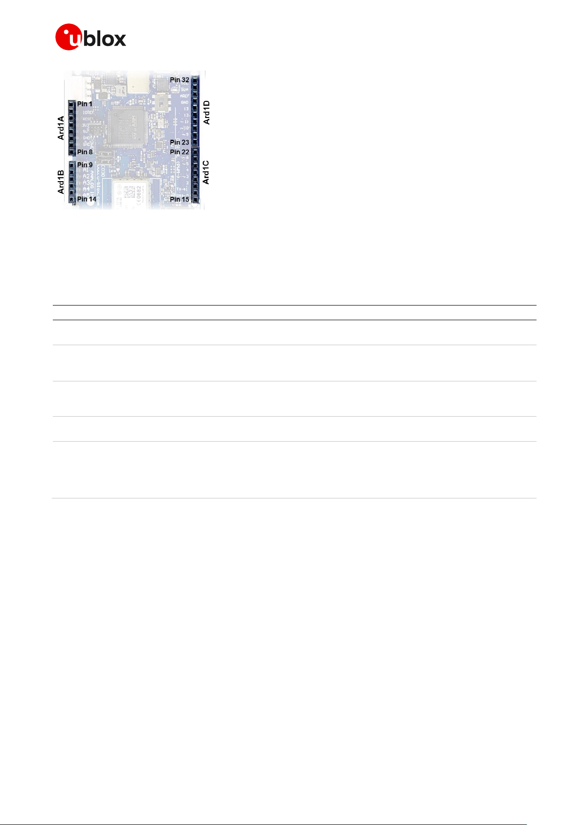
2.7 Arduino™ UNO R3 compatible interface pin out
C030 Arduino™ UNO R3 compatible interface details are given in Table 6 and depicted in Figure 18.
Conn.
Pin
N°
Arduino
naming
Description
HostMCU port assignment
Alternate functions and notes
Ard1A
1
n.c.
Not connected
2
IOREF
IO reference voltage level.
Connected to 3.3 VDC
Could be used as input for external
IO level setting.
3
nR
Reset signal input.
Negative logic
4
3.3V
3.3 VDC supply output
Controlled by HostMCU Port PE_0
0: Disable, 1:Enable
5
5V
5 VDC Reference input
Could be used as IO Reference
input
6
GND
Ground level
7
GND
Ground level
8
VIN
External DC supply input
In the range of 2.5 VDC to 5.5 VDC
See Jumper J1 in section 2.4
Ard1B
9
A0
Analog input
PA_3 Analog input7
GPIO, Ext. interrupt
10
A1
Analog input
PC_0 Analog input7
GPIO, Ext. interrupt
11
A2
Analog input
PC_3 Analog input7
GPIO, Ext. interrupt
12
A3
Analog input
PA_4 Analog input7
GPIO, Ext. interrupt
13
A4
Analog input
PA_6 Analog input7, PB_7 I2C1 SDA8
GPIO, Ext. interrupt
14
A5
Analog input
PB_0 Analog input7, PB_6 I2C1 SCL9
GPIO, Ext. interrupt
Ard1C
15
D0
Digital I/O, UART RX
PD_9, USART3_TX
GPIO, Ext. interrupt
16
D1
Digital I/O, UART TX
PD_8, USART3_RX
GPIO, Ext. interrupt
17
D2
Digital I/O
PD_11
USART3_CTS, GPIO, External
interrupt
18
D3
Digital I/O
PB_14
USART3_RTS, GPIO, PWM, Ext.
interrupt
19
D4
Digital I/O
PB_1
GPIO, PWM, Ext. interrupt
20
D5
Digital I/O
PA_5
GPIO, PWM, Ext. interrupt
21
D6
Digital I/O
PB_8
GPIO, PWM, Ext. interrupt
22
D7
Digital I/O
PB_15
GPIO, PWM, Ext. interrupt
Ard1D
23
D8
Digital I/O
PD_15
GPIO, Ext. interrupt
24
D9
Digital I/O
PD_12
GPIO, Ext. interrupt
25
D1010
Digital I/O
PE_11, SPI4 NSS, shared with SD Card
GPIO, PWM, Ext. interrupt
26
D11
Digital I/O
PE_6, SPI4 MOSI, shared with SD Card
GPIO, PWM, Ext. interrupt
27
D12
Digital I/O
PE_5, SPI4 MISO, shared with SD Card
GPIO, PWM, Ext. interrupt
28
D13
Digital I/O
PE_2, SPI4 SCK, shared with SD Card
GPIO, Ext. interrupt
29
GND
Ground level
30
AREF
3.3 VDC Reference
31
SDA
I2C SDA I/O
PB_6 I2C1 SCL
GPIO, Ext. interrupt
32
SCL
I2C SCL Output
PB_7 I2C1 SDA
GPIO, Ext. interrupt
Table 6: C030 Arduino UNO R3 compatible interface
7
Pin is connected to the port via 1 kΩ/1 kΩ resistive voltage divider.
8
PB_7 could be connected to the (A4) Ard1B Pin 13 to provide I2C1 SDA signal.
9
PB_6 could be connected to the (A5) Ard1B Pin 14 to provide I2C1 SCL signal.
10
Arduino interface D10 to D13 pins are used as an SPI Bus to HostMCU SPI4 peripheral. The D10 to D13 pins are shared with
the SD card socket.
Page 26
C030 - User guide
UBX-17015029 - R06 Hardware description Page 26 of 34
C1-Public
Figure 18: C030 Arduino™ UNO R3 connectors
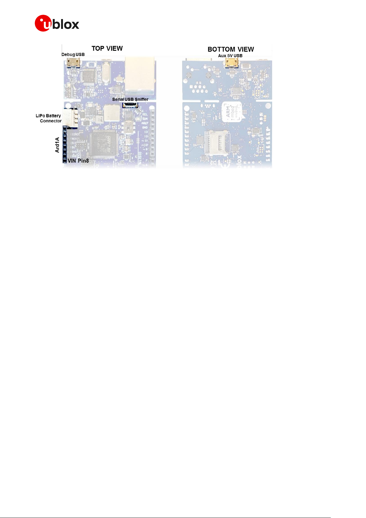
2.8 Power supply options and LiPo battery usage
The C030 can be powered up from several resources, individually or all together. The power supply
usage configurations are provided in Table 7.
#
Connector
Description
1
Debug USB
Uses development PC’s USB 5 VDC VBUS to power up the Utility and Application sections
of the C030. It charges up the LiPo battery if it is connected.
2
Aux 5V USB
Auxiliary USB power input. A USB power supply could be connected to power up only the
Application section of the C030.
It charges up the LiPo battery if it is connected. There is no communication functionality.
3
Serial USB sniffer
Uses Development PC’s USB 5 VDC VBUS to power up only the Application section of the
C030. It charges up the LiPo battery if it is connected. The serial USB sniffer circuitry could
only be powered from its dedicated USB connector.
4
LiPo battery
The C030 Application section could run only from a LiPo Battery connected. If one or many
of the #1, #2, #3 USB connections are available. The LiPo Battery is charged up as well.
5
Arduino™ UNO R3 VIN Pin 8
Arduino™ UNO R3 VIN pin 8 could be used to power up entire the C030 Application section
except serial USB sniffer circuitry. STLink (or CMSIS-DAP when available) feature could be
used through the debug USB. However, the C030 Application section including LiPo Battery
management circuitry is disconnected.
The VIN input voltage should be in the range of 2.5 VDC to 5.5 VDC.
Table 7: C030 power supply options and LiPo battery usage
☞ The C030 could run on a single supply input from #1 debug USB or #3 serial USB sniffer. However,
the cellular module transmission power demand might not be satisfied from these connections.
In such a use case, the C030 might be suffering brownout dues to USB VBUS supply rail cuts due
to USB current limitations. Therefore, either a 5 VDC USB power supply with ~3 ADC capacity
should be connected to the Aux 5V USB connector and/or an adequate LiPo battery, such as a BAK
LP-503759-IS-3, should be connected to the LiPo battery connector. The locations of the power
supply connections are shown in Figure 19. It is recommended to use LiPo battery in conjunction
to the USB connections as high frequency current demands might not be provided by the USB
VBUS rails but the LiPo battery
Page 27
C030 - User guide
UBX-17015029 - R06 Hardware description Page 27 of 34
C1-Public
Figure 19: C030 power supply connection options
2.9 C030-N211 variant cellular module firmware upgrade
When new firmware is available for the SARA-N211 cellular module, it is possible to upgrade the
firmware on the SARA-N211 that is on the C030-N211 board. For firmware upgrades, contact your local
u-blox representative.
Page 28

C030 - User guide
UBX-17015029 - R06 Getting started Page 28 of 34
C1-Public
3 Getting started
3.1 eUICC (embedded SIM) activation
☞ This section applies to the C030-U201 and C030-R3121 only.
The C030-U201 / C030-R3121 variants have an integrated eUICC (embedded SIM) for international
data roaming cellular connectivity service. The 50 MB of data or the 90-day period of cellular
connectivity service, whichever comes first, are covered in the C030-U201 / C030-R3121 package to
provide a seamless out-of-the-box experience.
The international data roaming connectivity service is provided by JT® JTGlobal. The service must be
activated through the Internet. The JT® international data roaming cellular connectivity service
activation procedure is provided below:
Visit http://www.jtiotsims.com/ubxC030 (the link is forwarded automatically to
https://jtiotsims.com/ubxC030/)
1. Register (or Login) to your account
2. Enter the C030-U201 / C030-R3121 IMSI code given on the C030-U201 / C030-R3121 board
3. Customize the PIN code or leave as default
4. Optionally name your IMSI for easier top up in the future
5. Accept the Terms and Conditions
6. Click “Activate” to start your connectivity service.
3.2 C030 board setup
1. (Omit for C030-U201 / C030-R3121) Insert the SIM card into the SIM connector/card holder.
2. (Omit for C030-N211) Connect the cellular antenna to the cellular main antenna SMA female
connector (ANT1)
3. (Optional) connect the Diversity cellular antenna to the cellular diversity antenna SMA female
connector (ANT2)
4. (Omit for C030-N211) Connect the GNSS antenna to the GNSS antenna SMA female.
5. Configure the C030 as described in section 2.2.
6. Power up the C030 board as described in section 2.8.
3.3 Development PC USB driver configuration
Although the USB drivers can be loaded by the development PC operating system automatically, it is
recommended to follow the guidelines mentioned below:
The debug USB port STLink/V2-1 interface needs a driver. These drivers are available at:
http://www.st.com/content/st_com/en/products/embedded-software/development-toolsoftware/stsw-link009.html.
Similarly, the cellular modem USB sniffer USB port interface needs a driver, which is available at:
http://www.silabs.com/products/interface/usb-bridges/classic-usb-bridges/device.cp2105
Page 29

C030 - User guide
UBX-17015029 - R06 Getting started Page 29 of 34
C1-Public
3.4 Getting started with Mbed
Up-to-date information on how to operate the C030 starter kit within the Mbed development
environment is available at:
• For the C030-U201 variant: https://developer.mbed.org/platforms/ublox-C030-U201/
(Link is forwarded automatically to the site https://os.mbed.com/platforms/ublox-C030-U201/)
• For the C030-N211 variant: https://developer.mbed.org/platforms/ublox-C030-N211/
(Link is forwarded automatically to the site https://os.mbed.com/platforms/ublox-C030-N211/)
• For C030-R410M variant: https://developer.mbed.org/platforms/ublox-C030-R410M/
(Link is forwarded automatically to the site https://os.mbed.com/platforms/ublox-C030-R410M/)
• For C030-R3121 variant: https://developer.mbed.org/platforms/ublox-C030-R3121/
(Link is forwarded automatically to the site https://os.mbed.com/platforms/ublox-C030-R3121/)
Page 30
C030 - User guide
UBX-17015029 - R06 Approvals Page 30 of 34
C1-Public
4 Approvals
4.1 C030-U201 European Conformance CE mark
The C030-U201 application board has been evaluated against the essential requirements of the
2014/53/EU Radio Equipment Directive.
In order to satisfy the essential requirements of the 2014/53/EU Radio Equipment Directive, the device
is compliant with the following standards:
• Radio Frequency spectrum use (Article 3.2):
o EN 301 511
o EN 301 908-1
o EN 301 908-2
o EN 303 413
• Electromagnetic Compatibility (Article 3.1b):
o EN 301 489-1
o EN 301 489-19
o EN 301 489-52
• Health and Safety (Article 3.1a)
o EN 62368-1
o EN 62311 and EN 62479
The conformity assessment procedure for C030-U201 application boards, referred to in Article 17 and
detailed in Annex III of Directive 2014/53/EU, has been followed.
Thus, the following marking is included in the product:
There are no restrictions for the commercialization of the C030-U201 application boards in all the
countries of the European Union.
⚠ Radiofrequency radiation exposure Information: this equipment complies with radiation exposure
limits prescribed for an uncontrolled environment for fixed and mobile use conditions. This
equipment should be installed and operated with a minimum distance of 20 cm between the
radiator and the body of the user or nearby persons. This transmitter must not be collocated or
operating in conjunction with any other antenna or transmitter except as authorized in the
certification of the product.
⚠ The gain of the system antenna(s) used for C030-U201 application boards (i.e. the combined
transmission line, connector, cable losses and radiating element gain) must not exceed 2.96 dBi
(in the 900 MHz band, i.e. GSM 900 or UMTS FDD-8 band), 7.85 dBi (in the 1800 MHz band, i.e.
GSM 1800 band), 11.84 dBi (in the 2100 MHz band, i.e. UMTS FDD-1 band) for mobile and fixed or
mobile operating configurations.
Page 31
C030 - User guide
UBX-17015029 - R06 Approvals Page 31 of 34
C1-Public
4.2 C030-N211 European Conformance CE mark
The C030-N211 application board has been evaluated against the essential requirements of the
2014/53/EU Radio Equipment Directive.
In order to satisfy the essential requirements of the 2014/53/EU Radio Equipment Directive, the device
is compliant with the following standards:
• Radio Frequency spectrum use (Article 3.2):
o EN 301 908-1
o EN 301 908-13
o EN 303 413
• Electromagnetic Compatibility (Article 3.1b):
o EN 301 489-1
o EN 301 489-19
o EN 301 489-52
• Health and Safety (Article 3.1a)
o EN 62368-1
o EN 62311 and EN 62479
The conformity assessment procedure for C030-N211 application boards, referred to in Article 17 and
detailed in Annex III of Directive 2014/53/EU, has been followed.
Thus, the following marking is included in the product:
There are no restrictions for the commercialization of the C030-N211 application boards in all the
countries of the European Union.
⚠ Radiofrequency radiation exposure Information: this equipment complies with radiation exposure
limits prescribed for an uncontrolled environment for fixed and mobile use conditions. This
equipment should be installed and operated with a minimum distance of 20 cm between the
radiator and the body of the user or nearby persons. This transmitter must not be collocated or
operating in conjunction with any other antenna or transmitter except as authorized in the
certification of the product.
⚠ The gain of the system antenna(s) used for C030-N211 application boards (i.e. the combined
transmission line, connector, cable losses and radiating element gain) must not exceed 9.2 dBi (in
the 800 MHz band, i.e. LTE band 20) and 9.4 dBi (in the 900 MHz band, i.e. LTE band 8) for mobile
and fixed or mobile operating configurations.
Page 32
C030 - User guide
UBX-17015029 - R06 Appendix Page 32 of 34
C1-Public
Appendix
A Glossary
Abbreviation
Definition
Arm
Arm (Advanced RISC Machines) Holdings
CE
Certification Mark for EHS compliance in the European Economic Area
CTS
Clear To Send
eUICC
embedded SIM
FDD
Frequency Division Duplex
GLONASS
Global Navigation Satellite System
GND
Ground
GNSS
Generic Navy Simulation System
GPIO
General Purpose Input Output
GSM
Global System for Mobile Communication
HSPA
High Speed Packet Access
I2C
Inter-Integrated Circuit
IMSI
International Mobile Station Identity
IoT
Internet of Things
LCC
Leadless Chip Carrier
LTE
Long Term Evolution
PCB
Printed Circuit Board
PIN
Personal Identification Number
PWM
Pulse Width Modulation
RAM
Random Access Memory
RTS
Request To Send
SCL
Serial Clock
SDA
Serial Data
SIM
Subscriber Identification Module
SiP
System in Package
SPI
Serial Peripheral Interface
UART
Universal Asynchronous Receiver-Transmitter
USB
Universal Serial Bus
Table 8: Explanation of the abbreviations and terms used
Page 33

C030 - User guide
UBX-17015029 - R06 Related documentation Page 33 of 34
C1-Public
Related documentation
[1] u-blox SARA-U2 series data sheet, UBX-13005287
[2] u-blox SARA-N2 series data sheet, UBX-15025564
[3] u-blox SARA-R4/SARA-N4 series data sheet, UBX-16024152
[4] u-blox LARA-R3121 data sheet, UBX-18007123
[5] u-blox nested design application note, UBX-16007243
☞ For regular updates to u-blox documentation and to receive product change notifications, register
on our homepage (www.u-blox.com).
Revision history
Revision
Date
Name
Comments
R01
13-Jul-2017
euyg
Initial release.
R02
29-Nov-2017
euyg
Updated C030-N211 and C030-U201 product status
R03
07-Mar-2018
euyg
Updated C030-U201 product status.
Added Approvals section
R04
23-Mar-2018
lpah
Updated C030-N211 product status.
R05
26-Oct-2018
lpah
Extended document applicability to C030-R410M / C030-R3121
R06
31-Jan-2021
alos
Updated C030-N211, C030-R410M, C030-R3121 product status
Page 34

C030 - User guide
UBX-17015029 - R06 Contact Page 34 of 34
C1-Public
Contact
For complete contact information, visit us at www.u-blox.com.
u-blox Offices
North, Central and South America
u-blox America, Inc.
Phone: +1 703 483 3180
E-mail: info_us@u-blox.com
Regional Office West Coast:
Phone: +1 408 573 3640
E-mail: info_us@u-blox.com
Technical Support:
Phone: +1 703 483 3185
E-mail: support@u-blox.com
Headquarters
Europe, Middle East, Africa
u-blox AG
Phone: +41 44 722 74 44
E-mail: info@u-blox.com
Support: support@u-blox.com
Asia, Australia, Pacific
u-blox Singapore Pte. Ltd.
Phone: +65 6734 3811
E-mail: info_ap@u-blox.com
Support: support_ap@u-blox.com
Regional Office Australia:
Phone: +61 3 9566 7255
E-mail: info_anz@u-blox.com
Support: support_ap@u-blox.com
Regional Office China (Beijing):
Phone: +86 10 68 133 545
E-mail: info_cn@u-blox.com
Support: support_cn@u-blox.com
Regional Office China (Chongqing):
Phone: +86 23 6815 1588
E-mail: info_cn@u-blox.com
Support: support_cn@u-blox.com
Regional Office China (Shanghai):
Phone: +86 21 6090 4832
E-mail: info_cn@u-blox.com
Support: support_cn@u-blox.com
Regional Office China (Shenzhen):
Phone: +86 755 8627 1083
E-mail: info_cn@u-blox.com
Support: support_cn@u-blox.com
Regional Office India:
Phone: +91 80 405 092 00
E-mail: info_in@u-blox.com
Support: support_in@u-blox.com
Regional Office Japan (Osaka):
Phone: +81 6 6941 3660
E-mail: info_jp@u-blox.com
Support: support_jp@u-blox.com
Regional Office Japan (Tokyo):
Phone: +81 3 5775 3850
E-mail: info_jp@u-blox.com
Support: support_jp@u-blox.com
Regional Office Korea:
Phone: +82 2 542 0861
E-mail: info_kr@u-blox.com
Support: support_kr@u-blox.com
Regional Office Taiwan:
Phone: +886 2 2657 1090
E-mail: info_tw@u-blox.com
Support: support_tw@u-blox.com
 Loading...