

Page 1
Abstract
This technical data sheet describes the BMD-341 stand-alone Bluetooth® low energy module. The
OEMs can embed their own application on top of the integrated Bluetooth low energy stack using
Nordic Semiconductor SDK or Arm® Mbed™ integrated development environment (IDE).
www.u-blox.com
UBX-19033643 - R03
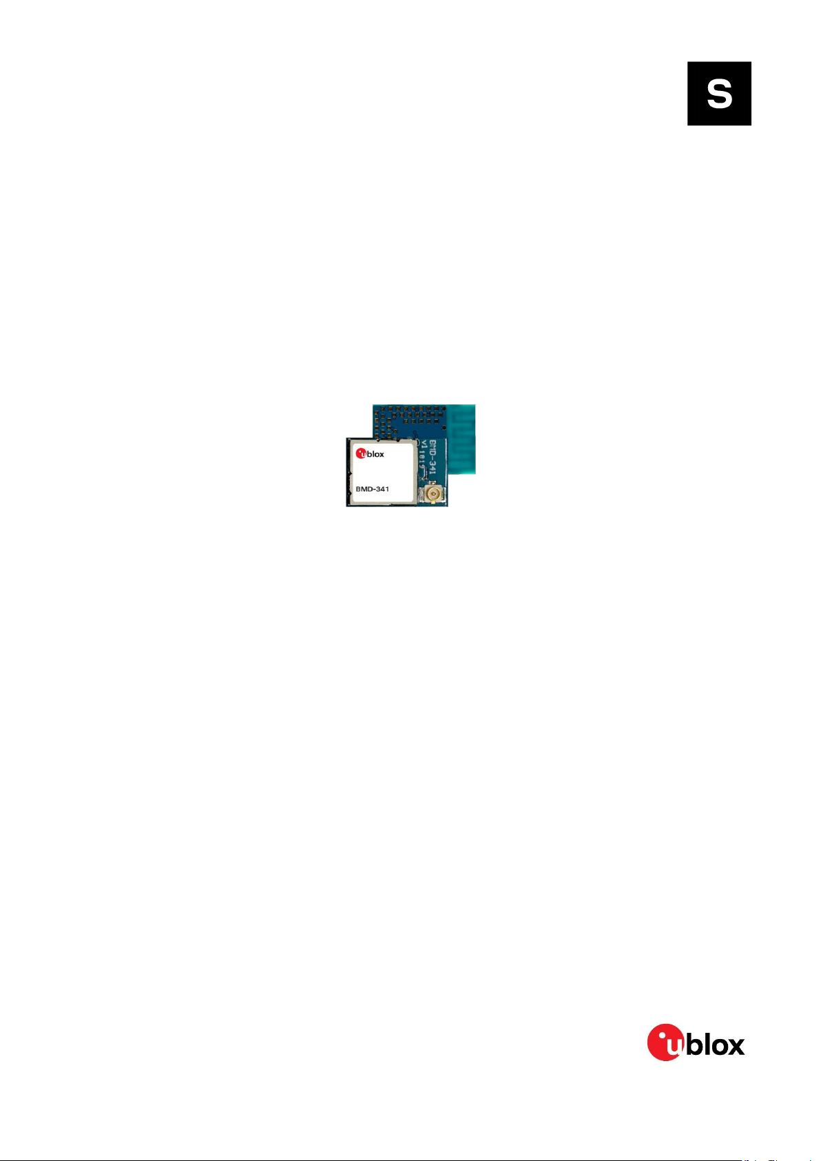
BMD-341
Stand-alone Bluetooth 5 low energy modules
Data sheet
Page 2
BMD-341 - Data sheet
Title
BMD-341
Subtitle
Stand-alone Bluetooth 5 low energy modules
Document type
Data sheet
Document number
UBX-19033643
Revision and date
R03
27-Sep-2019
Disclosure restriction
Product status
Corresponding content status
Functional sample
Draft
For functional testing. Revised and supplementary data will be published later.
In development /
Prototype
Objective specification
Target values. Revised and supplementary data will be published later.
Engineering sample
Advance information
Data based on early testing. Revised and supplementary data will be published later.
Initial production
Early production information
Data from product verification. Revised and supplementary data may be published later.
Mass production /
End of life
Production information
Document contains the final product specification.
Product name
Type number
Firmware version
PCN reference
Product status
BMD-341
BMD-341-A-R-00
N/A
N/A
Initial production
u-blox or third parties may hold intellectual property rights in the products, names, logos and designs included in this
document. Copying, reproduction, modification or disclosure to third parties of this document or any part thereof is only
permitted with the express written permission of u-blox.
The information contained herein is provided “as is” and u-blox assumes no liability for its use. No warranty, either express or
implied, is given, including but not limited to, with respect to the accuracy, correctness, reliability and fitness for a particular
purpose of the information. This document may be revised by u-blox at any time without notice. For the most recent
documents, visit www.u-blox.com.
Copyright © u-blox AG.
Document information
This document applies to the following products:
UBX-19033643 - R03 Document information Page 2 of 36
Page 3

BMD-341 - Data sheet
Contents
Document information ................................................................................................................................ 2
Contents .......................................................................................................................................................... 3
1 Functional description ......................................................................................................................... 5
1.1 Features ........................................................................................................................................................ 5
1.2 Applications ................................................................................................................................................. 6
1.3 Block diagram .............................................................................................................................................. 6
1.4 Radio performance ..................................................................................................................................... 7
2 Pin definition ........................................................................................................................................... 9
2.1 Pin assignment ............................................................................................................................................ 9
2.2 Peripheral pins ...........................................................................................................................................11
2.3 BMD-300 series footprint compatibility and migration ....................................................................12
2.3.1 BMD-300/301/330/360 to BMD-341 pad differences ..............................................................13
2.3.2 BMD-300/301/330/360 to BMD-341 design migration ...........................................................13
2.4 BMD-341 fan-out example ......................................................................................................................14
3 Electrical specifications ................................................................................................................... 15
3.1 Absolute maximum ratings ....................................................................................................................15
3.2 Operating conditions ................................................................................................................................15
3.3 Power and DCDC configuration ..............................................................................................................15
3.3.1 USB power ..........................................................................................................................................16
3.3.2 Normal (LV) power mode examples ..............................................................................................16
3.3.3 High voltage (HV) power mode examples ....................................................................................17
3.4 General purpose I/O ..................................................................................................................................18
3.5 Module reset ..............................................................................................................................................18
3.6 Debug and programming .........................................................................................................................19
3.7 Clocks ..........................................................................................................................................................19
3.7.1 32.768 kHz crystal (LFXO) ..............................................................................................................19
3.7.2 32.768 kHz clock source comparison ...........................................................................................19
4 Firmware ................................................................................................................................................ 20
4.1 Factory image ............................................................................................................................................20
4.2 SoftDevices ................................................................................................................................................20
4.2.1 S140 ....................................................................................................................................................20
4.2.2 S340 ....................................................................................................................................................20
4.2.3 IEEE 802.15.4 (Thread and Zigbee) ..............................................................................................21
4.3 Bluetooth address .....................................................................................................................................21
5 Mechanical specifications ............................................................................................................... 22
5.1 Dimensions .................................................................................................................................................22
5.2 Recommended PCB land pads ...............................................................................................................22
5.3 Module marking .........................................................................................................................................23
6 RF design notes ................................................................................................................................... 24
6.1 Recommended RF layout and ground plane ........................................................................................24
UBX-19033643 - R03 Contents Page 3 of 36
Page 4

BMD-341 - Data sheet
6.2 Mechanical enclosure ...............................................................................................................................24
6.3 Approved external antennas ..................................................................................................................24
7 BMD-341 evaluation development kit ......................................................................................... 25
8 Qualification and approvals............................................................................................................. 26
8.1 United States (FCC): ................................................................................................................................26
8.1.1 Labeling and user information requirements .............................................................................26
8.1.2 RF exposure .......................................................................................................................................26
8.2 Canada (ISED) ............................................................................................................................................27
8.2.1 Labeling and user information requirements .............................................................................27
8.2.2 RF exposure .......................................................................................................................................27
8.3 Europe (CE-RED) .......................................................................................................................................28
8.3.1 Labeling and user information requirements .............................................................................28
8.4 Australia / New Zealand (RCM) ..............................................................................................................28
8.5 Bluetooth qualification .............................................................................................................................28
9 Environmental...................................................................................................................................... 29
9.1 RoHS ............................................................................................................................................................29
9.2 REACH .........................................................................................................................................................29
9.3 California proposition 65 (P65) ..............................................................................................................29
10 Product handling ................................................................................................................................. 30
10.1 Packaging ...................................................................................................................................................30
10.2 Reel packaging ...........................................................................................................................................30
10.3 Carrier tape dimensions ..........................................................................................................................30
10.4 Moisture sensitivity level .........................................................................................................................30
10.6 Reflow soldering ........................................................................................................................................31
11 Labeling and ordering information ............................................................................................... 32
11.1 Batch Label .................................................................................................................................................32
11.2 Multipack label...........................................................................................................................................32
11.3 Ordering information ................................................................................................................................33
12 Support and other high-risk use warning .................................................................................. 34
Related documents ................................................................................................................................... 35
Revision history .......................................................................................................................................... 35
Contact .......................................................................................................................................................... 36
UBX-19033643 - R03 Contents Page 4 of 36
Page 5

BMD-341 - Data sheet
1 Functional description
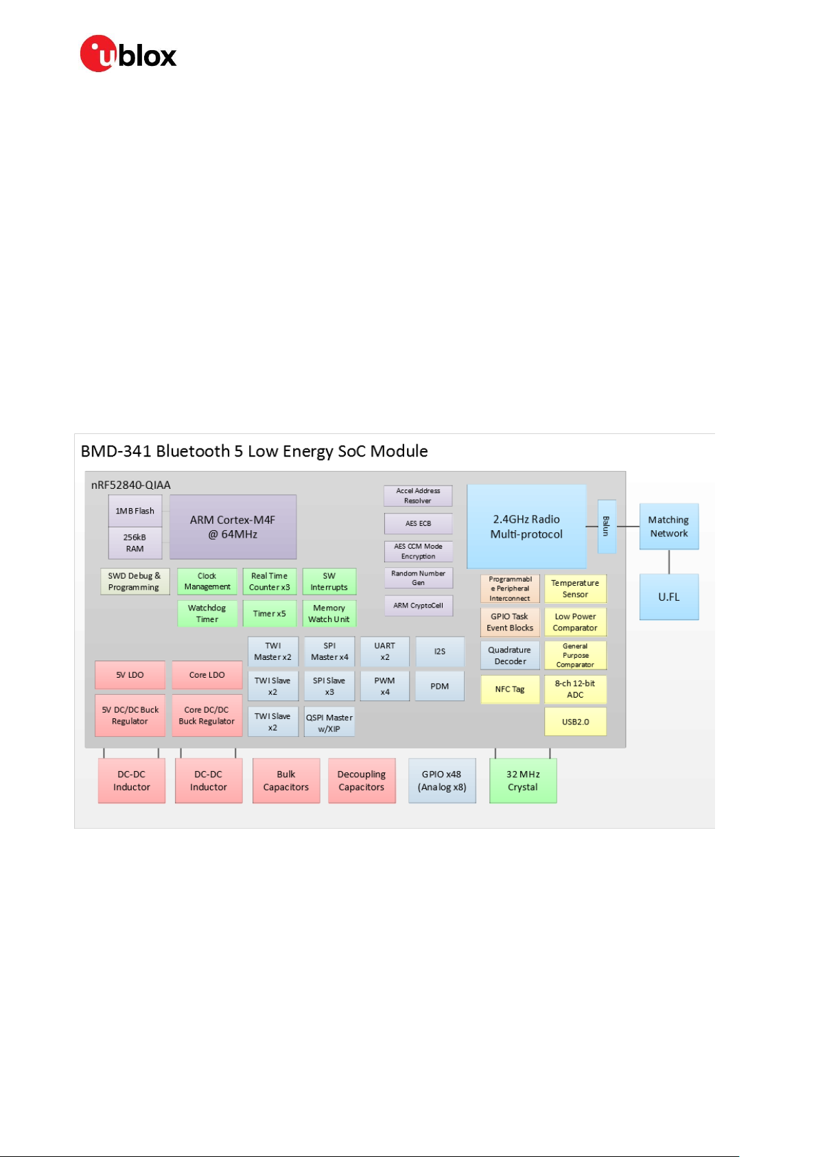
The BMD-341 is an advanced, highly flexible, ultra-low power multiprotocol SoM that enables
Bluetooth 5 (Bluetooth low energy) and IEEE 802.15.4 (Thread and Zigbee) connectivity for portable,
extremely low power embedded systems. With an ARM® Cortex™-M4F CPU, integrated 2.4 GHz
transceiver, and a U.FL connector for an external antenna, the BMD-341 provides a complete RF
solution allowing faster time to market with reduced development costs. Providing full use of the
Nordic Semiconductor nRF52840 capabilities and peripherals, the BMD-341 can power the most
demanding applications, all while simplifying designs and reducing BOM costs. The BMD-341 is an
ideal solution for designs that require the latest Bluetooth 5 features or 802.15.4 based networking
for Thread. Increased integration with built in USB and 5.5V compatible DC/DC supply reduces design
complexity and BOM cost, while expanding possible applications. BMD-341 designs are footprint
compatible with the BMD-300/301/330/360, providing low-cost flexibility for tiered product lineups.
1.1 Features
Based on the Nordic Semiconductor nRF52840 SoC
Bluetooth 5 2M low energy, Advertising Extensions, CSA #2, Coded PHY (Long Range)
Bluetooth mesh
IEEE 802.15.4 with Thread and Zigbee support
Complete RF solution with U.FL connector for an external antenna
Integrated DC-DC converter
No external components required
ARM® Cortex™-M4F 32-bit processor
ARM® TrustZone® Cryptocell 310 security
True random number generator
Serial Wire Debug (SWD)
Nordic Semiconductor SoftDevice ready
1 MB embedded flash memory
256 KB RAM
48 General Purpose I/O Pins
12-bit/200 KSPS ADC
One Full-Speed USB (12 Mbps)
Four SPI Master/Slave (8 Mbps)
Quad SPI with Execute in Place (XIP)
Low power comparator
Temperature sensor
Two 2-wire Master/Slave (I2C compatible)
I2S audio interface
Two UARTs (w/ CTS/RTS and DMA)
20 channel CPU independent Programmable Peripheral Interconnect (PPI)
Quadrature Demodulator (QDEC)
128-bit AES HW encryption
5 x 32 bit, 3 x 24 bit Real Timer Counters (RTC)
NFC-A tag interface for OOB pairing
Dimensions: 15.0 x 10.2 x 1.9 mm
UBX-19033643 - R03 Functional description Page 5 of 36
Page 6
BMD-341 - Data sheet
1.2 Applications
Climate control
Lighting products
Safety and security
Home appliances
Access control
Internet of Things
Home Health Care
Advanced Remote Controls
Smart Energy Management
Low-Power Sensor Networks
Interactive Entertainment Devices
Environmental Monitoring
Hotel Automation
Office Automation
1.3 Block diagram
Figure 1: Block diagram of BMD-341
UBX-19033643 - R03 Functional description Page 6 of 36
Page 7

BMD-341 - Data sheet
Detail
Description
Bluetooth
Bluetooth version
Bluetooth 5 Low Energy, Concurrent Central & Peripheral (S140)
Coded PHY (Long Range), 2 Mbps & 1 Mbps PHY, Advertising Extensions,
CSA #2, Bluetooth mesh
Security
AES-128
LE connections
Concurrent central, observer, peripheral, and broadcaster roles with up to
twenty concurrent connections along with one Observer and one
Broadcaster (S140)
IEEE 802.15.4
Thread stack
OpenThread, Thread 1.1 certified
Thread security
AES-128, ARM® Cryptocell accelerated
Zigbee stack
Zigbee 3.0 compliant
Radio
Frequency
2.360 GHz to 2.500 GHz
Modulations
GFSK at 1 Mbps and 2 Mbps, QPSK at 250 Kbps
Transmit power
+8 dBm maximum (at IC pin)
Receiver sensitivity
-96 dBm (BLE 1Mbps PHY)
Antenna
U.FL connector for an external antenna
Current consumption
TX only @ +8 dBm, 0 dBm @ 3V, DCDC enabled
14.8 mA, 4.8 mA
TX only @ +8 dBm, 0 dBm
32.7 mA, 10.6 mA
RX only @ 1 Mbps @ 3V, DCDC enabled
4.6 mA
RX only @ 1 Mbps
9.9 mA
CPU @ 64 MHz from flash, from RAM
6.3 mA, 5.2 mA
CPU @ 64 MHz from flash, from RAM @ 3V,
DCDC enabled
3.3 mA, 2.8 mA
System Off, On (Supply on VCC), no RAM
retention
0.4 µA, 0.97 µA
System Off, On (Supply on VCC), full 256 KB
RAM retention
1.86 µA, 2.35 µA
Dimensions
BMD-341
Length: 15.0 mm ± 0.3mm
Width: 10.2 mm ± 0.3mm
Height: 1.9 mm ± 0.1mm
Hardware
Interfaces
SPI Master/Slave x 4
Quad SPI x 1
UART x 2
Two-Wire Master/Slave (I2C) x 2
GPIO x 48
I2S x1
PWM x 12
PDM x 1
USB 2.0 x 1
Analog input x 8
Power supply
VCC: 1.7 V to 3.6 V, 1.75 V required to start DCDC
VCCH: 2.5 V to 5.5 V
VBUS: 4.35 V to 5.5 V (For USB operation)
1.4 Radio performance
UBX-19033643 - R03 Functional description Page 7 of 36
Page 8

BMD-341 - Data sheet
Detail
Description
Temperature range
-40 °C to +85 °C
Certifications
USA (FCC)
Canada (ISED)
Europe (CE) (Pending)
Australia / New Zealand (RCM) (Pending)
Bluetooth
FCC part 15.247 modular certification
FCC ID: XPYBMD341
Innovation, Science and Economic Development Canada RSS-247 modular
certification IC: 8595A-BMD341
EN 60950-1: A2:2013 3.1 (a): Health and Safety of the User
EN 301 489-1 V2.1.1 & 3.1 (b): Electromagnetic Compatibility
EN 301 489-17 V3.1.1
EN 300 328 V2.1.1 3.2: Effective use of spectrum allocated
AS/NZS 4268:2017, Radio equipment and systems – Short range devices
BMD-341 RF-PHY Component (Tested) – DID: D040773; QDID: 95452
Export
BMD-341
ECCN: 5A992.C, Exception 742.15(b)(1)
HTS: 8473.30.1180
Nordic Semiconductor nRF52840
nRF52840 Product Specification
nRF5 Software Development Kit
UBX-19033643 - R03 Functional description Page 8 of 36
Page 9
BMD-341 - Data sheet
No.
Name
I/O
Description
nRF52 pin
Remarks
1
GND
Power
Electrical Ground
GND
2
GND
Power
Electrical Ground
GND 3
GND
Power
Electrical Ground
GND 4
GND
Power
Electrical Ground
GND 5
GND
Power
Electrical Ground
GND 6
P0.25
I/O
GPIO
P0.25
7 P0.26
I/O
GPIO
P0.26
8 P0.27
I/O
GPIO
P0.27
9 P0.28
I/O
GPIO/AIN4
P0.28
Standard drive, low frequency I/O only (<10 kHz)
10
P0.29
I/O
GPIO/AIN5
P0.29
Standard drive, low frequency I/O only (<10 kHz)
11
P0.30
I/O
GPIO/AIN6
P0.30
Standard drive, low frequency I/O only (<10 kHz)
12
P0.31
I/O
GPIO/AIN7
P0.31
Standard drive, low frequency I/O only (<10 kHz)
13
P0.00
I/O
GPIO/XTAL1 (32.768 kHz)
P0.00
14
P0.01
I/O
GPIO/XTAL2 (32.768 KHz)
P0.01
15
P0.02
I/O
GPIO/AIN0
P0.02
Standard drive, low frequency I/O only (<10 kHz)
16
GND
Power
Electrical Ground
GND
17
VCC
Power
In/Out
LV Mode: 1.7 V to 3.6 V in
HV Mode: 1.8 V to 3.3 V
supply out1
VCC
An internal 4.7 µF bulk capacitor is included on
the module. However, it is good design practice to
add additional bulk capacitance as required for
your application, i.e. those with heavy GPIO usage
and/or current draw.
18
GND
Power
Electrical Ground
GND 19
P0.03
I/O
GPIO/AIN1
P0.03
Standard drive, low frequency I/O only (<10 kHz)
20
P0.04
I/O
GPIO/AIN2
P0.04
21
P0.05
I/O
GPIO/AIN3
P0.05
22
P0.06
I/O
GPIO
P0.06
23
P0.07
I/O
GPIO/TRACECLK
P0.07
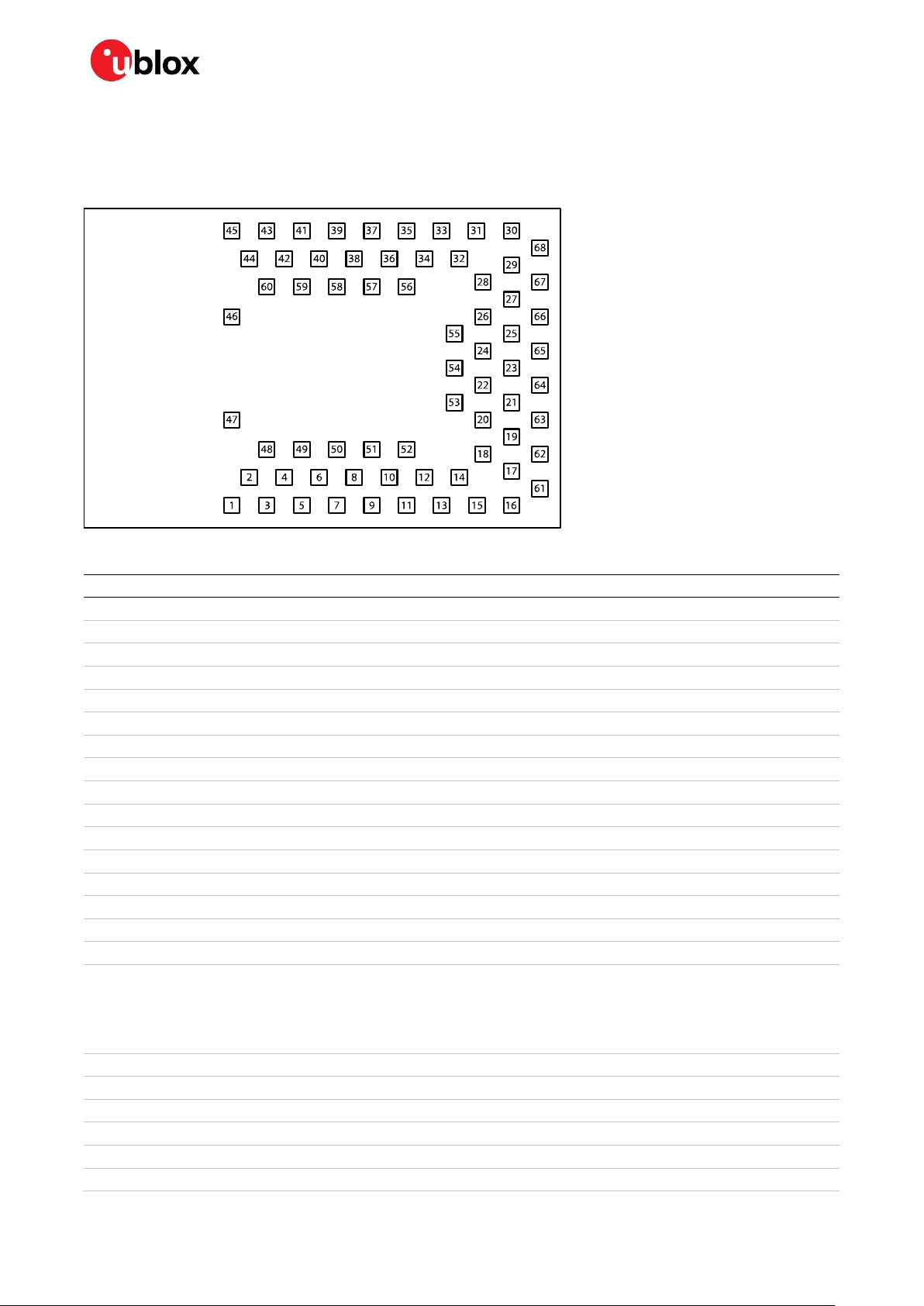
2 Pin definition
2.1 Pin assignment
Figure 2: BMD-341 Pin assignment (Top view)
UBX-19033643 - R03 Pin definition Page 9 of 36
Page 10

BMD-341 - Data sheet
No.
Name
I/O
Description
nRF52 pin
Remarks
24
P0.08
I/O
GPIO
P0.08
25
P0.09
I/O
GPIO/NFC1
P0.09
Standard drive, low frequency I/O only (<10 kHz)
26
P0.10
I/O
GPIO/NFC2
P0.10
Standard drive, low frequency I/O only (<10 kHz)
27
P0.11
I/O
GPIO/TRACEDATA[2]
P0.11
28
P0.12
I/O
GPIO/TRACEDATA[1]
P0.12
29
GND
Power
Electrical Ground
GND 30
GND
Power
Electrical Ground
GND 31
P0.13
I/O
GPIO
P0.13
32
P0.14
I/O
GPIO
P0.14
33
P0.15
I/O
GPIO
P0.15
34
P0.16
I/O
GPIO
P0.16
35
P0.17
I/O
GPIO
P0.17
36
P0.21
I/O
GPIO
P0.21
37
P0.19
I/O
GPIO
P0.19
38
P0.20
I/O
GPIO
P0.20
39
P0.18
I/O
GPIO/RESET_N
P0.18
40
P0.22
I/O
GPIO
P0.22
41
P0.23
I/O
GPIO
P0.23
42
P0.24
I/O
GPIO
P0.24
43
SWCLK
I
SWD Clock
SWCLK
44
SWDIO
I/O
SWD IO
SWDIO
45
GND
Power
Electrical Ground
GND 46
GND
Power
Electrical Ground
GND 47
GND
Power
Electrical Ground
GND 48
P1.05
I/O
GPIO
P1.05
Standard drive, low frequency I/O only (<10 kHz)
49
P1.06
I/O
GPIO
P1.06
Standard drive, low frequency I/O only (<10 kHz)
50
P1.07
I/O
GPIO
P1.07
Standard drive, low frequency I/O only (<10 kHz)
51
P1.08
I/O
GPIO
P1.08
52
P1.09
I/O
GPIO/TRACEDATA[3]
P1.09
53
P1.10
I/O
GPIO
P1.10
Standard drive, low frequency I/O only (<10 kHz)
54
P1.11
I/O
GPIO
P1.11
Standard drive, low frequency I/O only (<10 kHz)
55
GND
Power
Electrical Ground
GND
56
P1.00
I/O
GPIO/TRACEDATA[0]/SWO
P1.00
57
P1.01
I/O
GPIO
P1.01
Standard drive, low frequency I/O only (<10 kHz)
58
P1.02
I/O
GPIO
P1.02
Standard drive, low frequency I/O only (<10 kHz)
59
P1.03
I/O
GPIO
P1.03
Standard drive, low frequency I/O only (<10 kHz)
60
P1.04
I/O
GPIO
P1.04
Standard drive, low frequency I/O only (<10 kHz)
61
P1.12
I/O
GPIO
P1.12
Standard drive, low frequency I/O only (<10 kHz)
62
P1.13
I/O
GPIO
P1.13
Standard drive, low frequency I/O only (<10 kHz)
63
P1.14
I/O
GPIO
P1.14
Standard drive, low frequency I/O only (<10 kHz)
64
P1.15
I/O
GPIO
P1.15
Standard drive, low frequency I/O only (<10 kHz)
67
USB-D-
I/O
USB Data-
USB-D-
68
USB-D+
I/O
USB Data+
USB-D+
66
VBUS
Power
USB PHY supply: 4.35 V to
5.5 V in
VBUS
UBX-19033643 - R03 Pin definition Page 10 of 36
Page 11

BMD-341 - Data sheet
No.
Name
I/O
Description
nRF52 pin
Remarks
Connect to USB Host device 5
V supply
65
VCCH
Power
LV Mode: Connect to VCC
HV Mode: 2.5 V to 5.5 V in
VCCH
An internal 4.7 µF bulk capacitor is included on
the module. However, it is good design practice to
add additional bulk capacitance as required for
your application, i.e. those with heavy GPIO usage
and/or current draw.
Peripheral
Signal
Pin Options
UART0, UART1,
I2C0, I2C1,
SPI0, SPI1, SPI2, SPI3,
I2S0, QSPI0, PDN0,
PWM0, PWM1, PWM2, PWM3
All
P0.00-P0.31, P1.00-P1.15
ADC, COMP, LPCOMP
All
P0.02-P0.05, P0.28-P0.31 (AIN0-AIN7)
NFC
NFC1
NFC2
P0.09
P0.10
Reset
RESET_N
P0.18
Trace
TRACECLK
SWO/TRACEDATA[0]
TRACEDATA[1]
TRACEDATA[2]
TRACEDATA[3]
P0.07
P1.00
P0.12
P0.11
P1.09
SWD
SWD Clock
SWD IO
SWCLK
SWDIO
32.768 kHz Crystal
XTAL1
XTAL2
P0.00
P0.01
USB
USB Data +
USB Data -
USB-D+
USB-D-
Peripheral ID
Base Address
Shared Peripherals
3
0x40003000
SPI0
I2C0 4 0x40004000
SPI1
I2C1
Table 1: BMD-341 pin-out
1: In HV mode, VCC acts as a regulated supply that can power other external devices. The voltage output of VCC can be
configured in software but is limited to no more than VCCH-0.3 V. In System Off mode, VCC can supply no more than 1mA.
2.2 Peripheral pins
The BMD-341 features a pin multiplexing system that allows most internal peripherals, such as UART
and SPI, to be used on any GPIO pin. This freedom in pin choice enables better optimization of designs
and PCB layout. Note that only one peripheral signal can be multiplexed to a GPIO pin at a time. Some
functions are restricted to certain pins due to additional internal circuitry required by the interface.
These include: Trace signals, analog inputs, XTAL signals, USB signals, SWD interface, and reset. See
Table 2 for details:
Table 2: Peripheral pin options
☞ Some peripherals on the BMD-341 share the same memory location for their registers. This means
that only one of these peripherals can be used at a time. It is possible to switch between
peripherals sharing a register location by clearing and reinitializing the associated configuration
registers. See the Nordic Semiconductor nRF52840 Product Specification for details.
Table 3: Peripherals with shared registers
UBX-19033643 - R03 Pin definition Page 11 of 36
Page 12

BMD-341 - Data sheet
2.3 BMD-300 series footprint compatibility and migration
Figure 3: BMD-340/341 and BMD-300/301/330/360 Footprint comparison
The BMD-341 footprint is identical to the BMD-340 and has been designed to allow for backwards
compatibility with the BMD-300, BMD-301, BMD-330, and BMD-360 modules with pins 1 through 47
of the BMD-341 directly mapping to the same pin numbers on the BMD-300/301/330/360. This allows
BMD-300, BMD-301, BMD-330, and BMD-360 modules to be placed directly onto the BMD-341
footprint for easy migration and enabling tiered product design. Care should be taken to follow ground
plane and keep-out areas if designing for modules with an integrated antenna.
Generally, all pin names and functions remain the same, except for some differences noted below.
Pins 48 through 68 of the BMD-341 footprint are new pads used for new features that are not present
on the BMD-300/301/330/360 modules, such as USB interface and additional GPIO and power
connections.
Figure 4: BMD-300 Module soldered to BMD-340/341 footprint
UBX-19033643 - R03 Pin definition Page 12 of 36
Page 13

BMD-341 - Data sheet
Pin
BMD-300/301
Name
BMD-300/301
Function
BMD-341
Name
BMD-341
Function
39
P0.21
GPIO/RESET_N
P0.18
GPIO/RESET_N
38
P0.20
GPIO/TRACECLK
P0.20
GPIO
36
P0.18
GPIO/TRACEDATA[0]/SWO
P0.21
GPIO
34
P0.16
GPIO/TRACEDATA[1]
P0.16
GPIO
33
P0.15
GPIO/TRACEDATA[2]
P0.15
GPIO
32
P0.14
GPIO/TRACEDATA[3]
P0.14
GPIO
23
P0.07
GPIO
P0.07
GPIO/TRACECLK
56
N/A
N/A
P1.00
GPIO/TRACEDATA[0]/SWO
28
P0.12
GPIO
P0.12
GPIO/TRACEDATA[1]
27
P0.11
GPIO
P0.11
GPIO/TRACEDATA[2]
52
N/A
N/A
P1.09
GPIO/TRACEDATA[3]
New Pad VCCH:
Connect to VCC
2.3.1 BMD-300/301/330/360 to BMD-341 pad differences
Due to changes in the nRF52840 SoC used by the BMD-341, not all functions (such as SWO/TRACE
signals) are found on the same pins as on the BMD-300/301/330/360. Particularly of note is the reset
pin function which on the BMD-341 is now available on P0.18 instead of P0.21 as on the
BMD-300/301/330/360. To maintain pin for pin compatibility of the reset signal, P0.18 and P0.21
have swapped pad locations on the BMD-341 footprint. These differences are detailed in Table 4
below:
Table 4: BMD-300/301/330 to BMD-341 Pad differences
2.3.2 BMD-300/301/330/360 to BMD-341 design migration
Existing designs incorporating the BMD-300, BMD-301, BMD-330 or BMD-360 module can be
migrated over to the BMD-341 with the addition of a single footprint pad for VCCH (pin 65). This
migration option is only suitable for applications that do not require the new USB interface, additional
GPIO, or higher supply voltage functionality. The VCCH pad must be present and electrically
connected to the same supply as VCC for the module to operate correctly. Vias underneath the
BMD-341 should be tented to avoid shorts to unused module pads. Firmware written for the
BMD-300/301/330/360 can generally be ported to the BMD-341 with minimal effort. See the Nordic
Semiconductor SDK documentation for details.
Figure 5: BMD-300 to BMD-341 Migration Example
UBX-19033643 - R03 Pin definition Page 13 of 36
Page 14

BMD-341 - Data sheet
Top Layer
Bottom Layer
Figure 6: BMD-341 two-layer fan-out example
Using the BMD-341 minimal footprint, with only the additional VCCH pad added, allows BMD-300
designs to gain the following BMD-341 features with typically minor layout re-work:
Bluetooth 5 long range modes
IEEE 802.15.4 (Thread and Zigbee) connectivity
Doubled Flash memory (1 MB vs. 512 KB)
Quadrupled RAM (256 KB vs. 64 KB)
ARM® TrustZone® Cryptocell 310 security co-processor
To take advantage of new hardware features, such as the additional UART and Quad SPI interface,
the full BMD-341 footprint should be used. Designs that require the 5V DCDC converter, trace
interface, USB interface, or the additional GPIO (P1.00-P1.15) must use the full BMD-341 footprint.
☞ Since the BMD-300/301/330/360 can be soldered to the full BMD-340/341 footprint, it is
highly recommended that all new BMD-300/301/330/360 and BMD-340/341 projects use the
full
BMD-340/341 footprint. When migrating designs, the full BMD-341 footprint should be used
whenever possible as it is better suited for use with mass production SMT processing. Care
should be taken to follow ground plane and keep-out areas if designing for modules with an
integrated antenna.
2.4 BMD-341 fan-out example
The following figure is a BMD-341 fan-out example on a simple 2-layer PCB. This example is powered
via VCCH from a USB connection. See section 3.3 for details on power and DCDC operation.
UBX-19033643 - R03 Page 14 of 36
Page 15

BMD-341 - Data sheet
Symbol
Description
Min
Max
Unit
V
CC_MAX
Voltage on VCC supply pin
-0.3
3.9
V
V
CCH_MAX
Voltage on VCCH supply pin
-0.3
5.8 V V
BUS_MAX
Voltage on VBUS supply pin
-0.3
5.8 V V
IO_MAX
Voltage on GPIO pins (VCC > 3.6V)
-0.3
3.9 V V
IO_MAX
Voltage on GPIO pins (VCC ≤ 3.6V)
-0.3
VCC+0.3 V
V
TS
Storage Temperature Range
-40
125
°C
Symbol
Parameter
Min
Typ.
Max
Unit
V
CC_IN
VCC operating supply voltage in
1.7
3.0
3.6
V
V
CC_START
VCC DCDC starting voltage
1.75 - - V V
CCH_HV
VCCH operating supply voltage in
2.5
5.0
5.5
V
V
BUS_IN
VBUS operating supply voltage in
4.35
5.0
5.5
V
T
R_VCC
VCC Supply rise time (0 V to 1.7 V)
- - 60
ms
T
R_VCCH
VCCH Supply rise time (0 V to 3.7 V)
- - 100
ms
TA
Operating Ambient Temperature Range
-40
25
85
°C
3 Electrical specifications
⚠ Stressing the device above one or more of the ratings listed in the Absolute maximum rating
section may cause permanent damage. These are stress ratings only. Operating the module at
these or at any conditions other than those specified in the Operating conditions section of this
document should be avoided. Exposure to absolute maximum rating conditions for extended
periods may affect device reliability.
☞ Operating condition ranges define those limits within which the functionality of the device is
guaranteed. Where application information is given, it is advisory only and does not form part of
the specification.
3.1 Absolute maximum ratings
Table 5: Absolute maximum ratings
⚠ The product is not protected against overvoltage or reversed voltages. If necessary, voltage spikes
exceeding the power supply voltage specification, given in table above, must be limited to values
within the specified boundaries by using appropriate protection devices.
3.2 Operating conditions
☞ Unless otherwise specified, all operating condition specifications are at an ambient temperature
of 25 °C and a supply voltage of 3.3 V.
⚠ Operation beyond the specified operating conditions is not recommended and extended exposure
beyond them may affect device reliability.
Table 6: Operating conditions
3.3 Power and DCDC configuration
The BMD-341 has two internal regulator stages that each contain an LDO and DCDC regulator. The
first regulator, REG0, is fed by the VCCH pin and can accept a source voltage of 2.5 V to 5.5 V. The
output of REG0 is connected to the VCC pin and the input of the second regulator stage REG1. REG1
supplies power to the module core and can accept an input source voltage of 1.7 V to 3.6 V. Depending
on how the VCC and VCCH pins are connected, the module will operate in one of two modes:
UBX-19033643 - R03 Electrical specifications Page 15 of 36
Page 16

BMD-341 - Data sheet
Mode
Pin
Name
Connection
Normal (LV)
17
65
VCC
VCCH
1.7 V to 3.6 V source in
Same source as VCC
High Voltage (HV)
17
65
VCC
VCCH
1.8 V to 3.3 V supply out
2.5 V to 5.5 V source in
Normal/Low Voltage (LV) or High Voltage (HV). The voltage present on the VCC pin is always the GPIO
high logic level voltage, regardless of power mode.
To enter LV Mode, the same source voltage is applied to both the VCC and VCCH pins causing REG0
to automatically shut down leaving only the REG1 stage active. To enter HV, the source voltage is only
applied to VCCH causing the VCC pin to become an output source supplied by REG0.
Table 7: Power mode pin connections
⚠ Important: In both LV and HV mode, the GPIO logic level voltage is determined by the VCC pin. In
HV mode, all external devices that are connected to the BMD-341’s GPIO must either be powered
by the module (from VCC) or use level translation.
REG0 can supply a maximum current of 25 mA for the module and external circuits in System On
Mode and 1 mA in System Off Mode. External circuits powered from VCC in HV mode should be limited
to no more than 5 mA to ensure stability at all radio transmit power levels.
3.3.1 USB power
The USB interface on the BMD-341 can be used when the module is in either Normal (LV) or High
Voltage (HV) mode. The BMD-341 USB PHY is powered by a dedicated, internal LDO regulator that is
fed by the VBUS pin (66). This means that applying power to only the VBUS pin will not power the
rest of the module. In order for the USB PHY to operate, VBUS must be externally powered.
3.3.2 Normal (LV) power mode examples
Figure 7: BMD-340/341 LV Mode w/ Coin Cell Example
UBX-19033643 - R03 Electrical specifications Page 16 of 36
Page 17

BMD-341 - Data sheet
Figure 8: BMD-340/341 LV Mode w/ USB and external regulator
3.3.3 High voltage (HV) power mode examples
Figure 9: BMD-340/341 USB-powered HV mode example
UBX-19033643 - R03 Electrical specifications Page 17 of 36
Page 18

BMD-341 - Data sheet
Symbol
Parameter
Min.
Typ.
Max.
Unit
VIH
Input High Voltage
0.7 x VCC
-
VCC V VIL
Input Low Voltage
GND - 0.3 x VCC
V
VOH
Output High Voltage
VCC − 0.4
-
VCC V VOL
Output Low Voltage
GND - GND + 0.4
V
RPU
Pull-up Resistance
11
13
16
kΩ
RPD
Pull-down Resistance
11
13
16
kΩ
Figure 10: BMD-340/341 LiPo-powered HV example with USB charger
⚠ Important: The LiPo circuit above is meant to be a generic example of how the BMD-341’s power
modes can be used. Great care must be taken when integrating Lithium-Ion batteries into a
design. Protection circuits suitable for the type of battery used and the application must always
be implemented.
3.4 General purpose I/O
The general purpose I/O is organized as two ports enabling access and control of the 48 available GPIO
pins. The first port allows access of P0.00 to P0.31, similar to the one port available on the
BMD-300/301. The second port, new to the BMD-341, allows access to P1.00 to P1.15. Each GPIO can
be accessed individually with the following user configurable features:
Input/output direction
Output drive strength
Internal pull-up and pull-down resistors
Wake-up from high- or low-level triggers on all pins
Trigger interrupt on all pins
All pins can be used by the PPI task/event system; the maximum number of pins that can be
interfaced through the PPI at the same time is limited by the number of GPIOTE channels
All pins can be individually configured to carry serial interface or quadrature demodulator signals
Table 8: GPIO
3.5 Module reset
GPIO pin P0.18 may be used for a hardware reset. In order to utilize P0.18 as a hardware reset, the
UICR registers PSELRESET[0] and PSELRESET[1] must be set alike, to the value of 0x7FFFFFD2.
UBX-19033643 - R03 Electrical specifications Page 18 of 36
Page 19

BMD-341 - Data sheet
Symbol
Parameter
Typ.
Max.
Unit
F
NOM_LFXO
Crystal frequency
32.768
-
kHz
F
TOL_LFXO_BLE
Frequency tolerance, Bluetooth low energy applications
-
±500
ppm
f
TOL_LFXO_ANT
Frequency Tolerance, ANT applications
-
±50
ppm
C
L_LFXO
Load Capacitance
-
12.5
pF
C
0_LFXO
Shunt Capacitance
- 2 pF
R
S_LFXO
Equivalent series resistance
-
100
kΩ
C
pin
Input Capacitance on XL1 & XL2 pads
4 - pF
Symbol
Parameter
Min.
Typ.
Max.
Unit
I
LFXO
Current for 32.768 kHz Crystal Oscillator
-
0.23 - µA
I
LFRC
Current for 32.768 kHz RC Oscillator
-
0.7 1 µA
I
LFSYNT
Current for 32.768 kHz Synthesized Oscillator
-
100 - µA
f
TOL_LFXO_BLE
Frequency Tolerance, 32.768 kHz Crystal Oscillator (Bluetooth
low energy Stack)1
- - ±500
ppm
f
TOL_LFXO_ANT
Frequency Tolerance, 32.768 kHz Crystal Oscillator (ANT Stack)1
- - ±50
ppm
f
TOL_LFRC
Frequency Tolerance, 32.768 kHz RC Oscillator
- - ±5
%
f
TOL_CAL_LFRC
Frequency tolerance, 32.768 kHz RC after calibration
- - ±500
ppm
f
TOL_LFSYNT
Frequency Tolerance, 32.768 kHz Synthesized Oscillator
- - ±48
ppm
When P0.18 is programmed as RESET_N, the internal pull-up is automatically enabled. Nordic
Semiconductor example applications and development kits program P0.18 as RESET_N.
3.6 Debug and programming
The BMD-341 supports the two pin Serial Wire Debug (SWD) interface and offers flexible and powerful
mechanism for non-intrusive debugging of program code. Breakpoints, single stepping, and
instruction trace capture of code execution flow are part of this support.
The BMD-341 also supports ETM and ITM trace. The trace data from the ETM and the ITM is sent to
an external debugger via a 4-bit wide parallel trace port. In addition to parallel trace, the TPIU supports
serial trace via the Serial Wire Output (SWO) trace protocol.
3.7 Clocks
The BMD-341 requires two clocks, a high frequency clock and a low frequency clock. The high
frequency clock is provided on-module by a high-accuracy 32 MHz crystal as required by the
nRF52840 for radio operation.
The low frequency clock can be provided internally by an RC oscillator or synthesized from the fast
clock, or externally by a 32.768 kHz crystal. An external crystal provides the lowest power
consumption and greatest accuracy. Using the internal RC oscillator with calibration provides
acceptable performance for Bluetooth low energy applications at a reduced cost and slight increase
in power consumption.
☞ The ANT protocol requires the use of an external crystal.
☞ f
TOL_LFXO_BLE
applications. Actual tolerance depends on the crystal used.
3.7.1 32.768 kHz crystal (LFXO)
Table 9: 32.768 kHz Crystal (LFXO)
3.7.2 32.768 kHz clock source comparison
and f
TOL_LFXO_ANT
are the maximum allowed for Bluetooth low energy and ANT
Table 10 – 32.768 kHz Clock source comparison
UBX-19033643 - R03 Electrical specifications Page 19 of 36
Page 20

BMD-341 - Data sheet
4 Firmware
Projects for the BMD-341 should utilize the Nordic Semiconductor SDK and the nRF52840 tools for
new development. This will allow access to the very latest Bluetooth support from Nordic
Semiconductor and provide an ongoing path as new features are released.
4.1 Factory image
The BMD-341 module is not loaded with a factory firmware image.
4.2 SoftDevices
Nordic Semiconductor protocol stacks for Bluetooth and ANT are known as SoftDevices. SoftDevices
are pre-compiled, pre-linked binary files. SoftDevices can be programmed in nRF52 series SoCs and
are downloadable from the Nordic Semiconductor website. The BMD-341 with the nRF52840 SoC
supports the S140 (Bluetooth low energy Central & Peripheral) and S340 (ANT and Bluetooth low
energy) SoftDevices.
4.2.1 S140
The SoftDevice S140 is a feature complete Bluetooth 5 qualified protocol stack for the nRF52840
SoC. It supports up to 20 concurrent links in all roles. It supports Bluetooth 5 features: 2 Mbps, Long
Range, Advertising Extensions and channel selection algorithm #2. The number of connections and
bandwidth per connection are configurable, offering memory and performance optimization.
It is a complete stack with GAP, GATT, ATT, SM, L2CAP, and Link Layer. Both GATT Server and Client
are supported. The broad feature set also includes Privacy 1.2, LE Data Length Extension (DLE),
configurable ATT MTU, L2CAP connection-oriented channels and LE Secure Connections.
SoftDevice S140 is available for download here.
4.2.2 S340
SoftDevice S340 is a combined Bluetooth 5 and ANT™ protocol stack for the nRF52840 SoC,
supporting concurrent operation of the two.
It is a Bluetooth 5 qualified protocol stack that offers up to 20 concurrent links in all roles. It supports
all Bluetooth 5 features: 2 Mbps, Long Range, Advertising Extensions and channel selection algorithm
#2 (CSA #2). The number of connections and bandwidth per connection is configurable, offering
memory and performance optimization.
It is a complete Bluetooth LE stack with GAP, GATT, ATT, SM, L2CAP, and Link Layer. Both GATT
Server and Client are supported. The broad feature set also includes Privacy 1.2, LE Data Length
Extension (DLE), configurable ATT MTU, L2CAP connection-oriented channels and LE Secure
Connections.
It supports all ANT features and offers a variety of network topologies, including peer-to-peer, star
and tree. Up to 15 individual channels are available, with broadcast, acknowledged, or burst transfer
communication.
SoftDevice S340 is available for download here.
UBX-19033643 - R03 Firmware Page 20 of 36
Page 21

BMD-341 - Data sheet
UICR Register
Address
Description
NRF_UICR + 0x80
0x10001080
Bluetooth_addr [0] (0xCC)
NRF_UICR + 0x81
0x10001081
Bluetooth_addr [1] (0xBB)
NRF_UICR + 0x82
0x10001082
Bluetooth_addr [2] (0xAA)
NRF_UICR + 0x83
0x10001083
Bluetooth_addr [3] (0xEB)
NRF_UICR + 0x84
0x10001084
Bluetooth_addr [4] (0x1D)
NRF_UICR + 0x85
0x10001085
Bluetooth_addr [5] (0x6C)
4.2.3 IEEE 802.15.4 (Thread and Zigbee)
IEEE 802.15.4 based protocols, such as Thread and Zigbee, on the BMD-341 are not implemented
using a SoftDevice. Nordic Semiconductor provides an IEEE 802.15.4 compliant MAC stack which
does not require a SoftDevice to be loaded to operate. Nordic Semiconductor also provides
pre-compiled Thread and Zigbee stacks. See the Nordic Semiconductor SDK for more information on
developing applications that utilize IEEE 802.15.4. Both allow for concurrent operation with Bluetooth
low energy SoftDevices.
4.3 Bluetooth address
The BMD-341 modules are preprogrammed from the factory with a unique public Bluetooth address
stored in the UICR. The u-blox organizationally unique identifier is 6C:1D:EB. This is combined with
the last six characters of the Bluetooth address that are printed on a 2D barcode and in humanreadable text on the module label, as described in section 5.3 below.
Table 11: Bluetooth address
UBX-19033643 - R03 Firmware Page 21 of 36
Page 22

BMD-341 - Data sheet
5 Mechanical specifications
5.1 Dimensions
Figure 11: BMD-341 mechanical drawing
5.2 Recommended PCB land pads
Figure 12: Recommended PCB land pads
☞ There is no RF Keep-out area for BMD-341.
UBX-19033643 - R03 Mechanical specifications Page 22 of 36
Page 23

BMD-341 - Data sheet
Reference
Description
1
Date of unit production (year/week)
2
Product version
3
Product name
4
Data Matrix with unique serial number of 6 alphanumeric symbols, also in human-readable form. The full
Bluetooth address consists of the u-blox IEEE OUI (6C:1D:EB) with the six symbols appended:
6C:1D:EB:AA:BB:CC
1
2
4
3
5.3 Module marking
The labels of the BMD-341 modules include important product information, as described in this
section.
Figure 13 illustrates the label of the BMD-341 modules, which includes the u-blox logo, product
version, product name, Bluetooth address, and certification numbers.
Figure 13: Module marking
Table 12: BMD-341 label description
UBX-19033643 - R03 Mechanical specifications Page 23 of 36
Page 24

BMD-341 - Data sheet
#
Mfg.
Part Number
Max Gain
Type
Size
Approvals
1
Pulse
W1030
2 dBi
1/4 Wave Dipole – Whip
Length: 108.3mm
FCC, ISED, MIC
2
Taoglas
FXP73.07.0100A
2.5 dBi
1/4 Wave Dipole – Flex
7 mm x 47 mm x 0.1 mm
FCC, ISED, MIC
3
Pulse
W1027
3.2 dBi
1/4 Wave Dipole – Whip
Length: 136.8mm
FCC, ISED, MIC
4
Kinsun
6670113050-145
2.0 dBi
1/4 Wave Dipole – PCB
12 mm x 65 mm x 0.46 mm
FCC, ISED, MIC
6 RF design notes
6.1 Recommended RF layout and ground plane
Since the BMD-341 relies on an external antenna, there are no ground plane requirements or keep-out
area for the module itself. Refer to the external antenna datasheet for antenna placement and
grounding recommendations.
6.2 Mechanical enclosure
For the BMD-341, refer to the external antenna datasheet for placement in or on a mechanical
enclosure.
6.3 Approved external antennas
The antennas listed below were tested for use with the BMD-341.
Table 13: BMD-341 Approved external antennas
UBX-19033643 - R03 RF design notes Page 24 of 36
Page 25

BMD-341 - Data sheet
7 BMD-341 evaluation development kit
u-blox has developed full featured evaluation boards that provide a complete I/O pin out to headers,
on-board programming and debugging, 32.768 kHz crystal, power and virtual COM port over USB,
BMD-341 USB connector, 64 Mb quad SPI Flash, four user LEDs, and four user buttons. The
evaluation boards also provide the option to be powered from a CR2032 coin cell battery or a LiPo
battery through a JST-PH connecter and have current sense resistors and headers to allow for
convenient current measurements. Arduino Mega style headers are provided for easy prototyping of
additional functions. The evaluation boards also support programming off-board BMD-3xx series
modules.
Figure 14: BMD-341 evaluation board
UBX-19033643 - R03 BMD-341 evaluation development kit Page 25 of 36
Page 26

BMD-341 - Data sheet
8 Qualification and approvals
8.1 United States (FCC):
The BMD-341 module has received Federal Communications Commission (FCC) CFR47
Telecommunications, Part 15 Subpart C “Intentional Radiators” modular approval in accordance with
Parts 15.212 and 15.247. The modular approval allows the end user to integrate the module into a
finished product without obtaining subsequent and separate FCC approvals for intentional radiation,
provided no changes or modifications are made to the module circuitry. Changes or modifications
could void the user’s authority to operate the equipment. The end user must comply with all of the
instructions provided by the Grantee, which indicate installation and/or operating conditions
necessary for compliance.
The finished product is required to comply with all applicable FCC equipment authorizations
regulations, requirements and equipment functions not associated with the transmitter module
portion. For example, compliance must be demonstrated to regulations for other transmitter
components within the host product; to requirements for unintentional radiators (Part 15 Subpart B
“Unintentional Radiators”), such as digital devices, computer peripherals, radio receivers, etc.; and to
additional authorization requirements for the non-transmitter functions on the transmitter module
(that is, Verification, or Declaration of Conformity) (for example, transmitter modules may also
contain digital logic functions) as appropriate.
☞ Modification to this product will void the users’ authority to operate this equipment.
⚠ The OEM is still responsible for verifying end product compliance with FCC Part 15, subpart B
limits for unintentional radiators through an accredited test facility.
KDB 996369 D03 sections 2.4 (limited module procedures) and 2.5 (trace antenna designs) are not
applicable to the BMD-341.
8.1.1 Labeling and user information requirements
The BMD-341 is assigned the FCC ID number: XPYBMD341
If the FCC ID is not visible when the module is installed inside another device, then the outside of the
finished product into which the module is installed must also display a label referring to the enclosed
module. This exterior label can use the following or similar wording:
Contains FCC ID: XPYBMD341
In addition to marking the product with the appropriate FCC ID, the end product shall bear the
following statement in a conspicuous location on the device (FCC Rules, Title 47, Subchapter A, Part
15, Subpart B, Chapter §15.19):
This device complies with part 15 of the FCC Rules. Operation is subject to the following two
conditions: (1) This device may not cause harmful interference, and (2) this device must
accept any interference received, including interference that may cause undesired operation.
8.1.2 RF exposure
All transmitters regulated by FCC must comply with RF exposure requirements. KDB 447498 General
RF Exposure Guidance provides guidance in determining whether proposed or existing transmitting
facilities, operations or devices comply with limits for human exposure to Radio Frequency (RF) fields
adopted by the Federal Communications Commission (FCC).
This module is approved for installation into mobile and/or portable host platforms and must not be
co-located or operating in conjunction with any other antenna or transmitter except in accordance
UBX-19033643 - R03 Qualification and approvals Page 26 of 36
Page 27

BMD-341 - Data sheet
with FCC multi-transmitter guidelines. End users must be provided with transmitter operating
conditions for satisfying RF Exposure compliance.
8.2 Canada (ISED)
The BMD-341 module is certified for use in Canada under Innovation, Science and Economic
Development Canada (ISED) Radio Standards Specification (RSS) RSS-247 Issue 2 and RSSGen.
8.2.1 Labeling and user information requirements
The BMD-341 is assigned the IC ID number: 8595A-BMD341
Labeling Requirements for the Host Device (from Section 3.2.1, RSS-Gen, Issue 3, December 2010):
The host device shall be properly labeled to identify the module within the host device. The Industry
Canada certification label of a module shall be clearly visible at all times when installed in the host
device, otherwise the host device must be labeled to display the Industry Canada certification number
of the module, preceded by the words “Contains transmitter module”, or the word “Contains”, or
similar wording expressing the same meaning, as follows:
Contains transmitter module IC: 8595A-BMD341
User Manual Notice for License-Exempt Radio Apparatus (from Section 7.1.3 RSS-Gen, Issue 3,
December 2010): User manuals for license-exempt radio apparatus shall contain the following or
equivalent notice in a conspicuous location in the user manual or alternatively on the device or both:
This device complies with Industry Canada license exempt RSS standard(s). Operation is
subject to the following two conditions: (1) this device may not cause interference, and (2) this
device must accept any interference, including interference that may cause undesired
operation of the device.
Le présent appareil est conforme aux CNR d'Industrie Canada applicables aux appareils radio
exempts de licence. L'exploitation est autorisée aux deux conditions suivantes: (1) l'appareil
ne doit pas produire de brouillage, et (2) l'utilisateur de l'appareil doit accepter tout brouillage
radioélectrique subi, même si le brouillage est susceptible d'en compromettre le
fonctionnement.
Transmitter Antenna (from Section 7.1.2 RSS-Gen, Issue 3, December 2010): User manuals
for transmitters shall display the following notice in a conspicuous location:
Under Industry Canada regulations, this radio transmitter may only operate using an antenna
of a type and maximum (or lesser) gain approved for the transmitter by Industry Canada. To
reduce potential radio interference to other users, the antenna type and its gain should be so
chosen that the equivalent isotropically radiated power (e.i.r.p.) is not more than that
necessary for successful communication.
Conformément à la réglementation d'Industrie Canada, le présent émetteur radio peut
fonctionner avec une antenne d'un type et d'un gain maximal (ou inférieur) approuvé pour
l'émetteur par Industrie Canada. Dans le but de réduire les risques de brouillage radioélectrique
à l'intention des autres utilisateurs, il faut choisir le type d'antenne et son gain de sorte que la
puissance isotrope rayonnée équivalente (p.i.r.e.) ne dépasse pas l'intensité nécessaire à
l'établissement d'une communication satisfaisante.
8.2.2 RF exposure
All transmitters regulated by ISED must comply with RF exposure requirements listed in RSS-102 Radio Frequency (RF) Exposure Compliance of Radiocommunication Apparatus (All Frequency
Bands). This module is approved for installation into mobile host platforms and must not be colocated or operating in conjunction with any other antenna or transmitter except in accordance with
Industry Canada's multi-transmitter guidelines. A minimum 20 cm separation distance between any
UBX-19033643 - R03 Qualification and approvals Page 27 of 36
Page 28

BMD-341 - Data sheet
nearby person and the transmitter or antenna shall be maintained. End users must be provided with
transmitter operating conditions for satisfying RF Exposure compliance.
8.3 Europe (CE-RED)
The BMD-341 is a Radio Equipment Directive assessed radio module that is CE complaint and have
been manufactured and tested with the intention of being integrated into a final product.
The BMD-341 has been tested to current Radio Equipment Directives
EU - Radio Equipment Directive 2014/53/EU
ETSI EN 300 328 V 2.1.1
ETSI EN 301 489-1 V2.1.1
ETSI EN 301 489-17 V3.1.1
The Radio Equipment Directive – Compliance Association (RED-CA) provides guidance on modular
devices at the RED-CA website: http://www.redca.eu/Pages/Documents%201.htm.
8.3.1 Labeling and user information requirements
The label on the final products which contain a u-blox module must follow CE marking requirements.
The “R&TTE Compliance Association Technical Guidance Note 01” provides guidance on final product
CE marking.
8.4 Australia / New Zealand (RCM)
The BMD-341 has been tested to comply with the AS/NZS 4268:2017, Radio equipment and systems
– Short range devices – Limits and methods of measurement. The report may be obtained from your
local FAE., and may be used as evidence in obtaining permission to use the Regulatory Compliance
Mark (RCM).
Information on registration as a Responsible Party, license and labeling requirements may be found
at the following websites:
Australia: http://www.acma.gov.au/theACMA/radiocommunications-short-range-devices-standard-
2004
New Zealand: http://www.rsm.govt.nz/compliance
Only Australian-based and New Zealand-based companies who are registered may be granted
permission to use the RCM. An Australian-based or New Zealand-based agent or importer may also
register as a Responsible Party to use the RCM on behalf of a company not in Australia or New
Zealand.
8.5 Bluetooth qualification
The Bluetooth SIG maintains the Bluetooth Specification, and ensures that products are properly
tested and comply with the Bluetooth license agreements. Companies that list products with the
Bluetooth SIG are required to be members of the SIG and submit the listed fees. Refer to this link
for details: https://www.bluetooth.com/develop-with-bluetooth/qualification-listing
The BMD-341 Bluetooth low energy module based on the Nordic Semiconductor nRF52840 is
listed as a “Tested Component”, with Qualified Design IDs (QDID) 95452. This allows an endproduct based on a BMD-341 module to inherit the component listings without the need to run
through all of the tests again. The end-product will often inherit several QDIDs, and are identified
on a “Declaration of Compliance”. Refer to the BMD-3xx System Integration Manual for details on
creating an end product declaration.
The BMD-341 primarily utilizes the S140 SoftDevice.
UBX-19033643 - R03 Qualification and approvals Page 28 of 36
Page 29

BMD-341 - Data sheet
9 Environmental
9.1 RoHS
The BMD-341 module is in compliance with Directive 2011/65/EU, 2015/863/EU of the European
Parliament and the Council on the restriction of the use of certain hazardous substances in electrical
and electronic equipment.
9.2 REACH
BMD-341 modules do not contain the 201 SVHC (Substance of Very High Concern), as defined by
Directive EC/1907/2006 Article according to REACH Annex XVII.
9.3 California proposition 65 (P65)
This product can expose you to Nickel (metallic), which is known to the State of California to cause
cancer. For more information go to www.P65Warnings.ca.gov. Warnings are not required where the
listed chemical is inaccessible to the average user of the end product.
UBX-19033643 - R03 Environmental Page 29 of 36
Page 30

BMD-341 - Data sheet
10 Product handling
10.1 Packaging
10.2 Reel packaging
Modules are packaged on 330 mm reels loaded with 1000 modules. Each reel is placed in an antistatic
bag with a desiccant pack and humidity card and placed in a 340x350x65 mm box. An antistatic
warning and reel label are adhered to the outside of the bag.
Figure 15 – Reel cartons
10.3 Carrier tape dimensions
Figure 16 – Carrier tape dimensions
10.4 Moisture sensitivity level
The BMD-341 is rated for MSL 3, 168-hour floor life after opening.
UBX-19033643 - R03 Product handling Page 30 of 36
Page 31

BMD-341 - Data sheet
10.6 Reflow soldering
Figure 17: Reflow Profile for lead free solder
UBX-19033643 - R03 Product handling Page 31 of 36
Page 32

BMD-341 - Data sheet
11 Labeling and ordering information
11.1 Batch Label
Figure 18 shows an example of the layout and contents of the batch label. The label is affixed to reels,
sealed bags, and individual packing cartons (inner cartons).
Figure 18: Batch label example
11.2 Multipack label
Figure 19 shows an example of the layout and contents of the multipack label. The label is affixed to
shipping parcels (outer cartons).
UBX-19033643 - R03 Labeling and ordering information Page 32 of 36
Page 33

BMD-341 - Data sheet
Ordering Code
Product
BMD-341-A-R
BMD-341 module, Rev A, nRF52840-QIAA, Tape & Reel, 1000 piece multiples
BMD-341-EVAL
BMD-341-A Evaluation Kit w/ SEGGER J-Link-OB debug probe
Figure 19: Multipack label example
11.3 Ordering information
Table 14: Product ordering codes
UBX-19033643 - R03 Labeling and ordering information Page 33 of 36
Page 34

BMD-341 - Data sheet
12 Support and other high-risk use warning
This product is neither designed nor intended for use in a life support device or system, nor for use in
other fault-intolerant, hazardous or other environments requiring fail-safe performance, such as any
application in which the failure or malfunction of the product could lead directly or indirectly to death,
bodily injury, or physical or property damage (collectively, “high-risk environments”).
⚠ u-blox expressly disclaims any express or implied warranty of fitness for use in high-risk
environments.
The customer using this product in a high-risk environment agrees to indemnify and defend u-blox
from and against any claims and damages arising out of such use.
UBX-19033643 - R03 Support and other high-risk use warning Page 34 of 36
Page 35

BMD-341 - Data sheet
Revision
Date
Name
Comments
0.5
16-Apr-2019
Preliminary release for engineering samples.
1.0
01-Jul-2019
Updated Nordic Semiconductor links
Updated HV power output specifications
Updated RC Oscillator specifications
Updated images throughout
R03
27-Sep-2019
Document converted from Rigado to u-blox style data sheet.
Related documents
[1] u-blox Package Information Guide, Doc. No. UBX-14001652
[2] Nordic Semiconductor, nRF52840 Product Specification
[3] Nordic Semiconductor, nRF5 Software Development Kit
☞ For regular updates to u-blox documentation and to receive product change notifications, register
on our homepage (www.u-blox.com).
Revision history
UBX-19033643 - R03 Related documents Page 35 of 36
Page 36

BMD-341 - Data sheet
u-blox Offices
North, Central and South America
u-blox America, Inc.
Phone: +1 703 483 3180
E-mail: info_us@u-blox.com
Regional Office West Coast:
Phone: +1 408 573 3640
E-mail: info_us@u-blox.com
Technical Support:
Phone: +1 703 483 3185
E-mail: support@u-blox.com
Headquarters
Europe, Middle East, Africa
u-blox AG
Phone: +41 44 722 74 44
E-mail: info@u-blox.com
Support: support@u-blox.com
Asia, Australia, Pacific
u-blox Singapore Pte. Ltd.
Phone: +65 6734 3811
E-mail: info_ap@u-blox.com
Support: support_ap@u-blox.com
Regional Office Australia:
Phone: +61 2 8448 2016
E-mail: info_anz@u-blox.com
Support: support_ap@u-blox.com
Regional Office China (Beijing):
Phone: +86 10 68 133 545
E-mail: info_cn@u-blox.com
Support: support_cn@u-blox.com
Regional Office China (Chongqing):
Phone: +86 23 6815 1588
E-mail: info_cn@u-blox.com
Support: support_cn@u-blox.com
Regional Office China (Shanghai):
Phone: +86 21 6090 4832
E-mail: info_cn@u-blox.com
Support: support_cn@u-blox.com
Regional Office China (Shenzhen):
Phone: +86 755 8627 1083
E-mail: info_cn@u-blox.com
Support: support_cn@u-blox.com
Regional Office India:
Phone: +91 80 405 092 00
E-mail: info_in@u-blox.com
Support: support_in@u-blox.com
Regional Office Japan (Osaka):
Phone: +81 6 6941 3660
E-mail: info_jp@u-blox.com
Support: support_jp@u-blox.com
Regional Office Japan (Tokyo):
Phone: +81 3 5775 3850
E-mail: info_jp@u-blox.com
Support: support_jp@u-blox.com
Regional Office Korea:
Phone: +82 2 542 0861
E-mail: info_kr@u-blox.com
Support: support_kr@u-blox.com
Regional Office Taiwan:
Phone: +886 2 2657 1090
E-mail: info_tw@u-blox.com
Support: support_tw@u-blox.com
Contact
For complete contact information, visit us at www.u-blox.com.
UBX-19033643 - R03 Contact Page 36 of 36
 Loading...