

Ubiq QM3022M6 Schematic [ru]
General Description
The QM3022M6 is the highest performance trench
N-ch MOSFETs with extreme high cell density ,
which provide excellent RDSON and gate charge
for most of the synchronous buck converter
applications .
The QM3022M6 meet the RoHS and Green
Product requirement , 100% EAS guaranteed with
full function reliability approved.
Features
z Advanced high cell density Trench technology
z Super Low Gate Charge
z Excellent CdV/dt effect decline
z 100% EAS Guaranteed
z Green Device Available
Absolute Maximum Ratings
Symbol Parameter Rating Units
VDS Drain-Source Voltage 30 V
VGS
ID@TC=25℃
ID@TC=100℃
ID@TA=25℃
ID@TA=70℃
IDM Pulsed Drain Current2 160 A
EAS Single Pulse Avalanche Energy3 252 mJ
IAS Avalanche Current 48 A
PD@TC=25℃
PD@TA=25℃
T
Storage Temperature Range -55 to 150
STG
TJ Operating Junction Temperature Range -55 to 150
Continuous Drain Current, VGS @ 10V1 76 A
Continuous Drain Current, VGS @ 10V1 48 A
Continuous Drain Current, VGS @ 10V1 14 A
Continuous Drain Current, VGS @ 10V1 11.2 A
Gate-Source Voltage
Total Power Dissipation4 59.5 W
Total Power Dissipation4 2 W
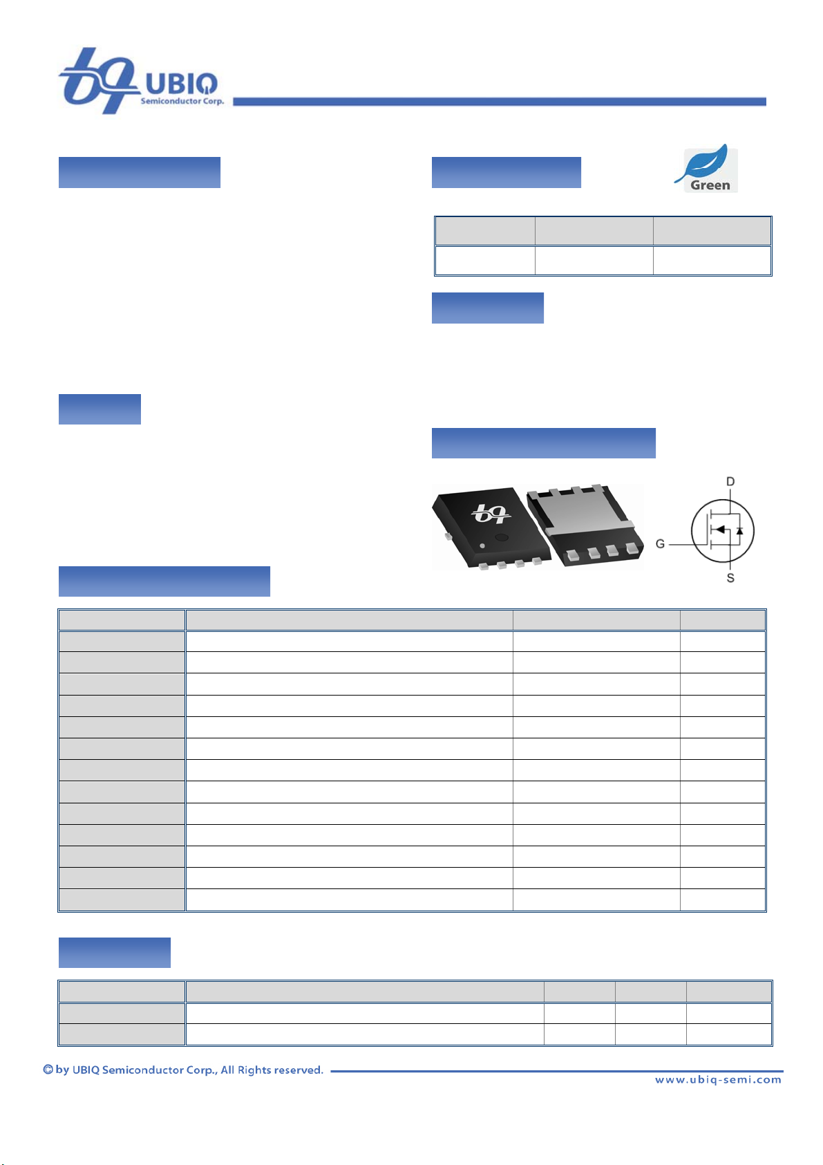
QM3022M6
N-Ch 30V Fast Switching MOSFETs
Product Summery
BVDSS RDSON ID
30V 7mΩ 76A
Applications
z High Frequency Point-of-Load Synchronous
Buck Converter for MB/NB/UMPC/VGA
z Networking DC-DC Power System
z Load Switch
PRPAK56 Pin Configuration
D
G
S
S
S
±20
V
℃
℃
Thermal Data
Symbol Parameter Typ. Max. Unit
R
Thermal Resistance Junction-ambient (Steady State)1 --- 62
θJA
R
Thermal Resistance Junction-Case1 --- 2.1
θJC
1
℃/W
℃/W
Rev A.01 D111210
QM3022M6
N-Ch 30V Fast Switching MOSFETs
Electrical Characteristics (TJ=25 ℃, unless otherwise noted)
Symbol Parameter Conditions Min. Typ. Max. Unit
BV
Drain-Source Breakdown Voltage VGS=0V , ID=250uA 30 --- --- V
DSS
△BV
/△TJ
BVDSS Temperature Coefficient
Static Drain-Source On-Resistance2
Gate Threshold Voltage
V
Temperature Coefficient --- -5.24 ---
GS(th)
Drain-Source Leakage Current
Gate-Source Leakage Current
R
V
△V
DSS
DS(ON)
GS(th)
GS(th)
I
DSS
I
GSS
Reference to 25℃ , ID=1mA
VGS=10V , ID=30A --- 5.5 7
VGS=4.5V , ID=15A --- 8.5 10.5
VGS=VDS , ID =250uA
=24V , VGS=0V , TJ=25℃
V
DS
VDS=24V , VGS=0V , TJ=55℃
V
=±20V , VDS=0V
GS
--- 0.028 ---
V/℃
mΩ
1.2 1.5 2.5 V
mV/℃
--- --- 1
uA
--- --- 5
--- ---
±100
nA
gfs Forward Transconductance VDS=5V , ID=30A --- 40 --- S
Rg Gate Resistance VDS=0V , VGS=0V , f=1MHz --- 1.9 3.8
Qg Total Gate Charge (4.5V)
=15V , VGS=4.5V , ID=15A
Qgs Gate-Source Charge --- 4.8 6.7
V
DS
--- 13.2 18.5
Ω
nC
Qgd Gate-Drain Charge --- 4.9 6.9
T
Turn-On Delay Time
d(on)
=15V , VGS=10V , RG=3.3Ω
Tr Rise Time --- 10.6 19
T
Turn-Off Delay Time --- 27 54
d(off)
V
DS
I
=15A
D
--- 5.4 10.8
ns
Tf Fall Time --- 7.6 15.2
C
Input Capacitance
iss
=15V , VGS=0V , f=1MHz
C
Output Capacitance --- 262 367
oss
C
Reverse Transfer Capacitance --- 138 193
rss
V
DS
--- 1512 2116
pF
Guaranteed Avalanche Characteristics
Symbol Parameter Conditions Min. Typ. Max. Unit
EAS Single Pulse Avalanche Energy5
VDD=25V , L=0.1mH , IAS=24A
63 --- --- mJ
Diode Characteristics
Symbol Parameter Conditions Min. Typ. Max. Unit
IS Continuous Source Current
ISM Pulsed Source Current
VSD Diode Forward Voltage2
1,6
2,6
--- --- 160 A
=0V , Force Current
V
G=VD
=0V , IS=1A , TJ=25℃
V
GS
trr Reverse Recovery Time
F=30A , dI/dt=100A/µs , T
Qrr Reverse Recovery Charge --- 4 --- nC
Note :
1.The data tested by surface mounted on a 1 inch
2.The data tested by pulsed , pulse width ≦ 300us , duty cycle ≦ 2%
3.The EAS data shows Max. rating . The test condition is V
4.The power dissipation is limited by 150℃ junction temperature
5.The Min. value is 100% EAS tested guarantee.
6.The data is theoretically the same as I
and IDM , in real applications , should be limited by total power dissipation.
D
2
FR-4 board with 2OZ copper.
I
=25V,VGS=10V,L=0.1mH,IAS=48A
DD
=25℃
J
2
--- --- 76 A
--- --- 1 V
--- 13 --- nS
 Loading...