

Tyco Safety Canada 123G260R Users Guide

HE863 Family
Hardware User Guide
1vv0300891 Rev.5 – 2011-03-18
P
H
E
-
EUDH
E
-
EURHE
-
EUGH
E
H
E
ARH
E
H
E
H
E
HE863 Family Hardware User Guide
1vv0300891 Rev.5
APPLICABLE PRODUCT
RODUCT
863
863
863
863-NAD
863-N
863-NAG
863-AUD
863-AUG
- 2011-03-18
Reproduction forbidden without Telit Communications S.p.A’s. written authorization - All Rights
Reserved. Page 2 of 89

HE863 Family Hardware User Guide
1vv0300891 Rev.5
- 2011-03-18
Disclaimer
The information contained in this document is the proprietary
information of Telit Communications S.p.A. and its affiliates
(“TELIT”).
The contents are confidential and any disclosure to persons
other than the officers, employees, agents or subcontractors
of the owner or licensee of this document, without the prior
written consent of Telit, is strictly prohibited.
Telit makes every effort to ensure the quality of the
information it makes available. Notwithstanding the foregoing,
Telit does not make any warranty as to the information
contained herein, and does not accept any liability for any
injury, loss or damage of any kind incurred by use of or
reliance upon the information.
Telit disclaims any and all responsibility for the
application of the devices characterized in this document, and
notes that the application of the device must comply with the
SAFETY standards of the applicable country, and where
applicable, with the relevant wiring rules.
Telit reserves the right to make modifications, additions and
deletions to this document due to typographical errors,
inaccurate information, or improvements to programs and/or
equipment at any time and without notice.
Such changes will, nevertheless be incorporated into new
editions of this document.
Copyright: Transmittal, reproduction, dissemination and/or
editing of this document as well as utilization of its
contents and communication thereof to others without express
authorization are prohibited. Offenders will be held liable
for payment of damages. All rights are reserved.
Copyright © Telit Communications S.p.A. 2010.
Reproduction forbidden without Telit Communications S.p.A’s. written authorization - All Rights
Reserved. Page 3 of 89

HE863 Family Hardware User Guide
1vv0300891 Rev.5
- 2011-03-18
Contents
1. INTRODUCTION.................................................................................................................................................6
1.1. S
1.2. A
1.3. C
1.4. D
1.5. T
1.6. R
1.7. D
COPE............................................................................................................................... ..................................6
UDIENCE............................................................................................................................................................6
ONTACT INFORMATION, SUPPORT...................................................................................................................6
OCUMENT ORGANIZATION................................................................................................................................7
EXT CONVENTIONS...........................................................................................................................................8
ELATED DOCUMENTS.......................................................................................................................................8
OCUMENT HISTORY..........................................................................................................................................9
2. OVERVIEW.......................................................................................................................................................11
2.1. HE863
FAMILYPRODUCTSPECIFICATION...................................................................................................................12
3. HE863FAMILYMECHANICALDIMENSIONS.......................................................................................................14
4. HE863FAMILYMODULECONNECTIONS...........................................................................................................15
4.1. HE863-EUD/NAD/AUD
4.2. HE863-EUR/NAR
4.3. HE863-EUG/NAG/AUG
4.4. BALLS
LAYOUT.............................................................................................................................................30
PIN-OUT................................................................................................................15
PIN-OUT..........................................................................................................................20
PIN-OUT................................................................................................................25
5. HARDWARECOMMANDS.................................................................................................................................31
5.1. T
5.2. I
5.3. T
URNING ON THE HE863................................................................................................................................31
NITIALIZATION AND ACTIVATION STATE............................................................................................................31
URNING OFF THE HE863..............................................................................................................................34
5.3.1. Hardware Unconditional Restart.........................................................................................................36
5.4. S
UMMARY OF TURNING ON AND OFF THE HE863.........................................................................................37
6. POWERSUPPLY................................................................................................................................................38
6.1. P
6.2. G
OWER SUPPLY REQUIREMENTS.....................................................................................................................38
ENERAL DESIGN RULES.................................................................................................................................40
6.2.1. Electrical Design Guidelines................................................................................................................40
6.2.1.1. +5VInputSourcePowerSupplyDesignGuidelines...............................................................................................40
6.2.1.2. +12VInputSourcePowerSupplyDesignGuidelines.............................................................................................41
6.2.2. Thermal Design Guidelines..................................................................................................................43
6.2.3. Power Supply PCB Layout Guidelines...............................................................................................44
7. ANTENNA(S)....................................................................................................................................................46
7.1. GSM/WCDMA
7.2. GSM/WCDMA
7.3. GSM/WCDMA
7.4. GPS
7.5. GPS
7.6. GPS
ANTENNA REQUIREMENTS (HE863-EUG/NAG/AUG ONLY)................................................................53
ANTENNA-PCB LINE GUIDELINES (HE863-EUG/NAG/AUG ONLY)....................................................54
ANTENNA-INSTALLATION GUIDELINES (HE863-EUG/NAG/AUG ONLY)..............................................58
ANTENNA REQUIREMENTS.....................................................................................................46
ANTENNA – PCB LINE GUIDELINES........................................................................................47
ANTENNA – INSTALLATION GUIDELINES.................................................................................52
8. LOGICLEVELSPECIFICATIONS...........................................................................................................................59
8.1. R
ESET SIGNAL..................................................................................................................................................60
9. SERIALPORTS..................................................................................................................................................61
Reproduction forbidden without Telit Communications S.p.A’s. written authorization - All Rights
Reserved. Page 4 of 89

HE863 Family Hardware User Guide
1vv0300891 Rev.5
9.1. MODEM SERIAL PORT.......................................................................................................................................61
9.2. RS232
10. USBPORT....................................................................................................................................................65
LEVEL TRANSLATION............................................................................................................................63
- 2011-03-18
10.1. USB
TRANSCEIVER SPECIFICATIONS (TBD)....................................................................................................65
11. AUDIOSECTION(HE863‐EUR/EUG/NAR/NAG/AUGONLY)............................................................................66
11.1. S
11.2. M
ELECTION MODE..............................................................................................................................................66
ICROPHONE CHARACTERISTICS.....................................................................................................................68
11.2.1. Input Lines (MIC1 and MIC2) Characteristics (TBD)........................................................................68
11.3. OUTPUT
LINES (SPEAKER)...........................................................................................................................68
11.3.1. Output Lines Characteristics (TBD)....................................................................................................69
12. GENERALPURPOSEI/O................................................................................................................................70
12.1. L
12.2. U
12.3. U
12.4. U
12.5. I
12.6. RTC
12.7. VAUX1
OGIC LEVEL SPECIFICATIONS.........................................................................................................................72
SING A GPIO PAD AS INPUT..........................................................................................................................72
SING A GPIO PAD AS OUTPUT......................................................................................................................72
SING THE ALARM OUTPUT GPIO6.................................................................................................................73
NDICATION OF NETWORK SERVICE AVAILABILITY...........................................................................................73
BYPASS OUT............................................................................................................................................74
POWER OUTPUT..................................................................................................................................74
13. DACANDADCSECTION................................................................................................................................76
13.1. DAC
CONVERTER.............................................................................................................................................76
13.1.1. Description............................................................................................................................... ...............76
13.1.2. Enabling DAC............................................................................................................................... ..........76
13.1.3. Low Pass Filter Example......................................................................................................................77
13.2. ADC
CONVERTER.............................................................................................................................................77
13.2.1. Description............................................................................................................................... ...............77
13.2.2. Using ADC Converter............................................................................................................................77
14. MOUNTINGTHEHE863FAMILYONYOURBOARD........................................................................................78
14.1. G
ENERAL...........................................................................................................................................................78
14.1.1. Recommended footprint for the application....................................................................................... 78
14.1.2. Suggested Inhibit Area..........................................................................................................................79
14.1.3. Stencil............................................................................................................................... .......................79
14.1.4. PCB Pad Design....................................................................................................................................79
14.1.5. Solder paste...........................................................................................................................................80
14.1.6. HE863 Family Solder Reflow...............................................................................................................81
14.2. DEBUG
OF THE HE863 FAMILY IN PRODUCTION...................................................................................82
15. SIMHOLDERDESIGNGUIDE.........................................................................................................................83
15.1. O
15.2. SIM
VERVIEW.........................................................................................................................................................83
INTERFACE.................................................................................................................................................84
16. ANTENNADETECTIONDESIGNGUIDE...........................................................................................................86
17. CONFORMITYASSESSMENTISSUES(TBD).....................................................................................................87
18. SAFETYRECOMMENDATIONS......................................................................................................................88
Reproduction forbidden without Telit Communications S.p.A’s. written authorization - All Rights
Reserved. Page 5 of 89
1. Introduction
1.1. Scope
The aim of this document is the description of some hardware
solutions useful for developing a product with the Telit
HE863-EUD/NAD/AUD/EUG/NAG/AUG/EUR/NAR module. All the features
and solutions detailed are applicable to all HE863 family,
whereas “family” is intended the modules listed in the
applicability table.
When a specific feature is applicable to a specific product,
it will be clearly highlighted.
HE863 Family Hardware User Guide
1vv0300891 Rev.5
- 2011-03-18
1.2. Audience
This document is intended for Telit customers, who are
integrators, about to implement their applications using our
HE863-EUD/NAD/AUD/EUG/NAG/AUG/EUR/ NAR
1.3. Contact Information, Support
For general contact, technical support, to report
documentation errors and to order manuals, contact Telit’s
Technical Support Center (TTSC) at:
TS-EMEA@telit.com
TS-NORTHAMERICA@telit.com
TS-LATINAMERICA@telit.com
TS-APAC@telit.com
Alternatively, use:
http://www.telit.com/en/products/technical-supportcenter/contact.php
For detailed information about where you can buy the Telit
modules or for recommendations on accessories and components
visit:
module.
http://www.telit.com
To register for product news and announcements or for product
questions contact Telit’s Technical Support Center (TTSC).
Our aim is to make this guide as helpful as possible. Keep us
informed of your comments and suggestions for improvements.
Telit appreciates feedback from the users of our information.
Reproduction forbidden without Telit Communications S.p.A’s. written authorization - All Rights
Reserved. Page 6 of 89

HE863 Family Hardware User Guide
1.4. Document Organization
This document contains the following chapters:
1vv0300891 Rev.5
- 2011-03-18
Chapter 1: “Introduction”
target audience, contact and support information, and text
conventions.
Chapter 2: “Overview”
Chapter 3: “HE863 Family Mechanical Dimensions”
layout.
Chapter 4: “HE863 Family Module Connections”
Chapter 5: “Hardware Commands ”
hardware
Chapter 6: ”Power Supply”
Chapter 7: “Antenna(s)”
layout design are the most important parts in the full product
design
Chapter 8: “Logic Level specifications”
adopted in the implementation of logic levels for this module.
Chapter 9: “Serial ports”
Chapter 10: “USB Port”
Chapter 11: “Audio Section ”
electrical characteristics of the Base Band Chip .
Chapter 12: “General Purpose I/O”
pads can be configured.
Chapter 13 “DAC and ADC Section”
converters.
provides a scope for this document,
provides an overview of the document.
deals with the
How to control the module via
deals on supply and consumption.
The antenna connection and board
Specific values
Refers to the audio blocks and
How the general purpose I/O
Deals with these two kind of
Chapter 14 “Mounting the HE863 Family on your board”
Chapter 15 “SIM holder design guide”
Reproduction forbidden without Telit Communications S.p.A’s. written authorization - All Rights
Reserved. Page 7 of 89
HE863 Family Hardware User Guide
1vv0300891 Rev.5
Chapter 16 “Antenna detection design guide”
- 2011-03-18
Chapter 17: “Conformity Assessments Issues”
fundamental hints about the conformity assessment that the
final application might need.
Chapter 18: “Safety Recommendations”
recommendations that must be followed by the customer in the
design of the application that makes use of the HE863 Family.
1.5. Text Conventions
Danger – This information MUST be followed or catastrophic
equipment failure or bodily injury may occur.
Caution or Warning – Alerts the user to important points about
integrating the module, if these points are not followed, the
module and end user equipment may fail or malfunction.
Tip or Information – Provides advice and suggestions that may
be useful when integrating the module.
provides some
provides some safety
All dates are in ISO 8601 format, i.e. YYYY-MM-DD.
1.6. Related Documents
HE863 Product Description
HE863 AT Command Manual
Reproduction forbidden without Telit Communications S.p.A’s. written authorization - All Rights
Reserved. Page 8 of 89
CChhaannggees
1.7. Document History
HE863 Family Hardware User Guide
1vv0300891 Rev.5
- 2011-03-18
RReevviissiioonn
Rev.0 2010-07-23 First issue
Rev.1 2010-07-27 Updated 4 HE863-EUD Modules Connections
Rev.2 2010-10-13 Added HE863-NAD/AUD/EUG/NAG/AUG characteristics
Rev.3 2010-11-24 Added HE863-EUR/NAR
Rev.4 2011-02-23 Updated 4.1 HE863-EUD/NAD/AUD PIN-OUT
Rev.5 2011-03-18 Updated 5.1 Turning ON the HE863
DDaatte
e
Updated 4.1 PIN-OUT
Updated 5.2 Initialization and Activation state(TBD)
Updated 5.3 Turning off the HE863-EUD
Updated 5.4 Summary of Turning ON and OFF the HE863EUD(TBD)
Updated 8.1 Reset Signal
Updated 14 SIM holder design guides
Removed 17.1 The schematics of the HE863 interface board
Added 2.1 HE863 Family Product Specification
Added 7.4 GPS Antenna Requirements(HE863-EUG/NAG/AUG
only)
Added 7.5 GPS Antenna-PCB Line Guidelines(HE863EUG/NAG/AUG only)
Added 7.6 GPS Antenna-Installation Guidelines(HE863EUG/NAG/AUG only)
Added 11 AUDIO Section(HE863-EUG/NAG/AUG only)
Added 13 DAC and ADC section
Updated 4 HE863 Family Modules Connections
Updated 5.2 Initialization and Activation state
Updated 6.1 Power Supply Requirements
Updated 7 Antenna(s)
Updated 9.2 RS232 Level Translation
Renumbered chapters.
Updated 1 Introduction
Updated 2.1 HE863 Family Product Specification
Updated 4 HE863 Family Modules Connections
Updated 6.1 Power Supply Requirements
Updated 7 GSM/WCDMA Antenna Requirements
Updated 11 AUDIO Section(HE863-EUR/EUG/NAR/NAG/AUG only)
Updated 4.2 HE863-EUR/NAR PIN-OUT
Updated 4.3 HE863-EUG/NAG/AUG PIN-OUT
Updated 5.1 Turning On the HE863
Removed 5.4 Summary of Turning ON and OFF
Updated 6.1 Power Supply Requirements
Updated 6.2.2 Thermal Design Guidelines
Updated 8.1 Reset Signal
Updated 11 Audio Section
Updated 12 General Purpose I/O
Updated 13 DAC And ADC Section
Updated 15.2 SIM interface
Added 16 Antenna detection design guide
s
Reproduction forbidden without Telit Communications S.p.A’s. written authorization - All Rights
Reserved. Page 9 of 89

HE863 Family Hardware User Guide
1vv0300891 Rev.5
Updated 5.2 Initialization and Activation state
Updated 5.3 Turning OFF the HE863
Added 5.4 Summary of Turning ON and OFF
Updated 7.2 GSM/WCDMA Antenna – PCB line Guidelines
Updated 7.3 GSM/WCDMA Antenna – Installation Guidelines
Updated 7.5 GPS Antenna – PCB line Guidelines(HE863EUG/NAG/AUG only)
Updated 15.2 SIM interface
Updated 17 Conformity Assessment Issues
- 2011-03-18
Reproduction forbidden without Telit Communications S.p.A’s. written authorization - All Rights
Reserved. Page 10 of 89

2. Overview
The aim of this document is the description of some hardware
solutions useful for developing a product with the Telit HE863
Family module.
In this document all the basic functions of a M2M device will
be taken into account; for each one of them a proper hardware
solution will be suggested and eventually the wrong solutions
and common errors to be avoided will be evidenced. Obviously
this document cannot embrace the whole hardware solutions and
products that may be designed. The wrong solutions to be
avoided must be considered as mandatory, while the suggested
hardware configurations must not be considered mandatory,
instead the information given must be used as a guide and a
starting point for properly developing your product with the
Telit HE863 Family module.
HE863 Family Hardware User Guide
1vv0300891 Rev.5
- 2011-03-18
.
NOTICE:
The integration of the GSM/GPRS/EDGE/UMTS/HSPA HE863 Family
cellular module within user application must be done according
to the design rules described in this manual.
The information presented in this document is believed to be
accurate and reliable. However, no responsibility is assumed
by Telit Communication S.p.A. for its use, such as any
infringement of patents or other rights of third parties which
may result from its use. No license is granted by implication
or otherwise under any patent rights of Telit Communication
S.p.A. other than for circuitry embodied in Telit products.
This document is subject to change without notice.
Reproduction forbidden without Telit Communications S.p.A’s. written authorization - All Rights
Reserved. Page 11 of 89

F
HE863-
EUGH
HE863 Family Hardware User Guide
1vv0300891 Rev.5
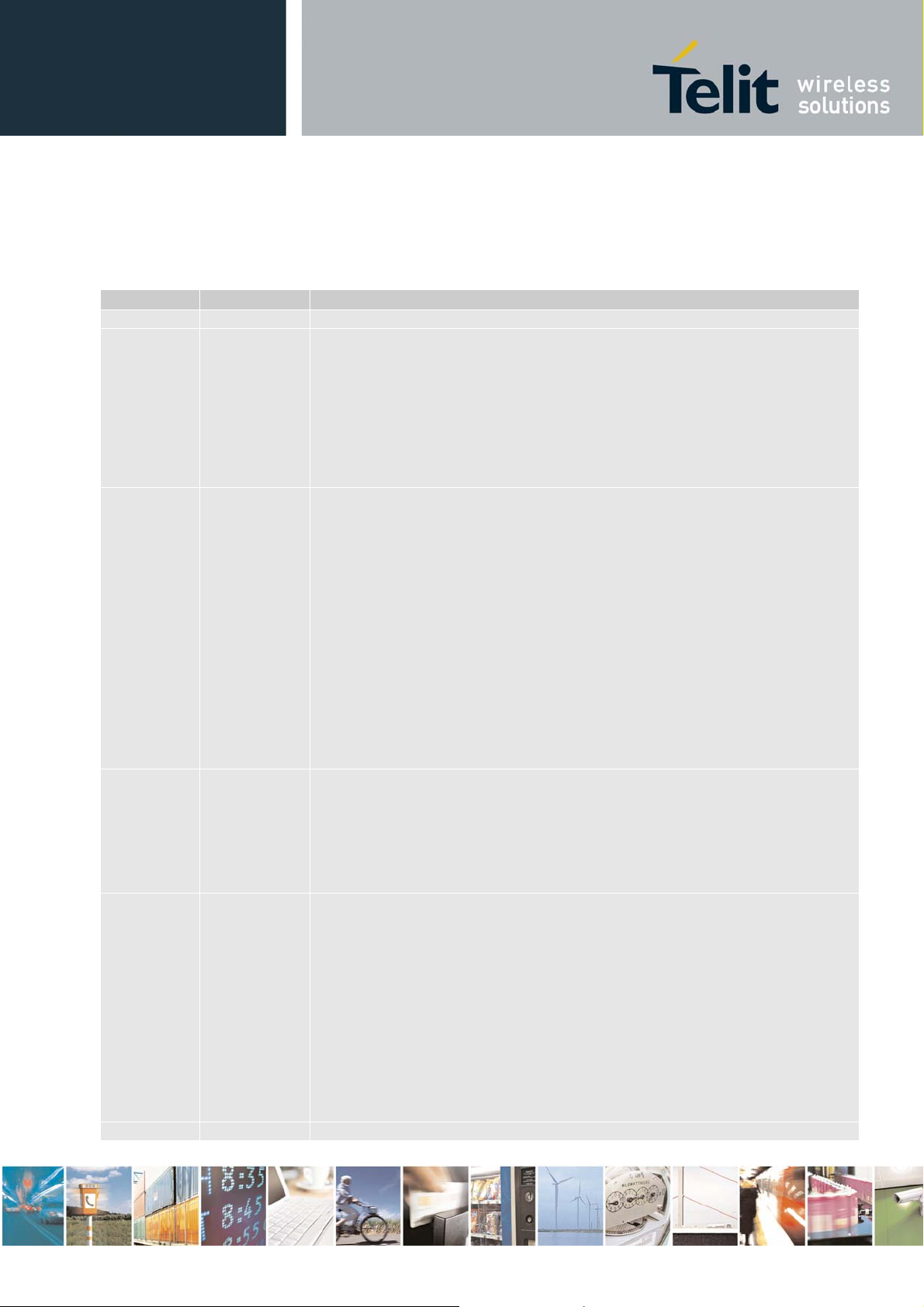
2.1. HE863 Family Product Specification
ITEM
Air
interfac
e
HE863-EUD HE863-EUR
▪ Dual-band
UMTS/HSPA
2100/900
▪ Quad-Band
GSM850/900
/1800/1900
▪ Data only
▪ Dual-band
UMTS/HSPA
2100/900
▪ Quad-Band
GSM850/900
/1800/1900
▪ Dual-band
UMTS/HSPA
2100/900
▪ Quad-Band
GSM850/900
/1800/1900
▪ Standalone
GPS
EATURE
E863-NAD HE863-NAR HE863-NAG
▪ Dual-band
UMTS/HSPA
1900/850
▪ Quad-Band
GSM850/900
/1800/1900
▪ Data only
▪ Dual-band
UMTS/HSPA
1900/850
▪ Quad-Band
GSM850/900
/1800/1900
- 2011-03-18
▪ Dual-band
UMTS/HSPA
1900/850
▪ Quad-Band
GSM850/900
/1800/1900
▪ Standalone
GPS
Size
Data
Service
Interfac
e
Antenna
Audio
41.4(L)X31.4(W)X2.9(T)
▪ HSPA UL 5.8Mbps, DL 7.2Mbps
▪
EDGE UL 118kbps, DL 236.8Kbps,
GPRS UL 42.8kbps, DL 85.6 Kbps
▪
▪ 189 Balls Grid Array interface
▪ 22 general I/O ports maximum including multi-functional I/Os
▪ Status LED output
▪ 3 A/D converters
▪ 1 D/A converter (PWM output)
▪ Full RS232 CMOS UART: baud rate up to 6Mbps
▪ Reserved two wires CMOS UART for debugging
▪ USB 2.0, baud rate up to 480Mbps
▪ 1.8V/3V SIM interface
External Antenna
▪ 2 pairs of analog audio interface
▪ PCM interface for Digital audio
(Audio only for HE863-EUG/EUR/NAG/NAR/AUG)
Message
SIM Card
Reproduction forbidden without Telit Communications S.p.A’s. written authorization - All Rights
Reserved. Page 12 of 89
SMS (MO/MT)
Support 1.8 and 3V UICC
F
HE863 Family Hardware User Guide
1vv0300891 Rev.5
- 2011-03-18
ITEM
Air
interfac
e
Size
Data
Service
Interfac
e
EATURE
HE863-AUD HE863-AUG
▪ Dual-band
UMTS/HSPA
2100/850
▪ Quad-Band
GSM850/900
/1800/1900
▪ Data only
41.4(L)X31.4(W)X2.9(T)
▪ HSPA UL 5.8Mbps, DL 7.2Mbps
▪
EDGE UL 118kbps, DL 236.8Kbps,
GPRS UL 42.8kbps, DL 85.6 Kbps
▪
▪ 189 Balls Grid Array interface
▪ 22 general I/O ports maximum including multi-functional I/Os
▪ Status LED output
▪ 3 A/D converters
▪ 1 D/A converter (PWM output)
▪ Full RS232 CMOS UART: baud rate up to 6Mbps
▪ Reserved two wires CMOS UART for debugging
▪ USB 2.0, baud rate up to 480Mbps
▪ 1.8V/3V SIM interface
▪ Dual-band
UMTS/HSPA
2100/850
▪ Quad-Band
GSM850/900
/1800/1900
▪ Standalone
GPS
Antenna
External Antenna
▪ 2 pairs of analog audio interface
Audio
▪ PCM interface for Digital audio
(Audio only for HE863-EUG/EUR/NAG/NAR/AUG)
Message
SIM Card
SMS (MO/MT)
Support 1.8 and 3V UICC
Reproduction forbidden without Telit Communications S.p.A’s. written authorization - All Rights
Reserved. Page 13 of 89
HE863 Family Hardware User Guide
1vv0300891 Rev.5
3. HE863 Family Mechanical Dimensions
The Telit HE863 Family module overall dimensions are:
• Length: 41.4 mm
• Width: 31.4 mm
• Thickness: 2.9 mm
- 2011-03-18
Reproduction forbidden without Telit Communications S.p.A’s. written authorization - All Rights
Reserved. Page 14 of 89
HE863 Family Hardware User Guide
1vv0300891 Rev.5
4. HE863 Family Module Connections
The HE863 Family features a 189 Balls Grid Array: in the following
sections a description of the available signals and their position in
the balls layout is presented.
4.1. HE863-EUD/NAD/AUD PIN-OUT
- 2011-03-18
Ball Signal I/O Function
SIM card interface
H11 SIMCLK O External SIM signal – Clock 1.8 / 3V
G12 SIMRST O External SIM signal – Reset 1.8 / 3V
F12 SIMIO I/O External SIM signal - Data I/O 1.8 / 3V
E12 SIMIN(TBD) I
H12 SIMVCC -
USB_SIM_D+
F11
(TBD)
USB_SIM_D-
G11
(TBD)
N4 TX_TRACE O Tx data for diagnostic monitor CMOS 1.8V
External SIM signal – Presence
(active low)
External SIM signal – Power
supply for the SIM
USB SIM(RESERVED)
I/O USB SIM data (+), TBD 1.8V/3.0V
I/O USB SIM data (-), TBD 1.8V/3.0V
Trace
Internal
Pull up
1.8
1.8 / 3V
Type
N3 RX_TRACE I Rx data for diagnostic monitor CMOS 1.8V
Prog. / Data + HW Flow Control
C125/RING
M4
(TBD)
C109/DCD
M3
(TBD)
C108/DTR
L3
(TBD)
C107/DSR
L4
(TBD)
Reproduction forbidden without Telit Communications S.p.A’s. written authorization - All Rights
Reserved. Page 15 of 89
Output for Ring indicator
signal (RI) to DTE
O
Output for Data set ready
O
signal (DSR) to DTE
Input for Data terminal ready
I
signal (DTR) from DTE
Output for Data set ready
O
signal (DSR) to DTE
CMOS 1.8V
CMOS 1.8V
CMOS 1.8V
CMOS 1.8V

Ball Signal I/O Function
HE863 Family Hardware User Guide
1vv0300891 Rev.5
Internal
Pull up
- 2011-03-18
Type
K4 C106/CTS O
K3 C105/RTS I
Output for Clear to send signal
(CTS) to DTE
Input for Request to send
signal (RTS) from DTE
CMOS 1.8V
CMOS 1.8V
J4 C104/RXD O Serial data output to DTE CMOS 1.8V
J3 C103/TXD I
Serial data input (TXD) from
DTE
CMOS 1.8V
USB
S8 USB_VBUS
S9 USB_ID(TBD) AI
Power supply for the internal
USB transceiver
Analog input used to sense
whether a peripheral device is
5V
Analog
connected.
R9 USB_D+ I/O USB differential Data (+) 3.3V
R8 USB_D- I/O USB differential Data (-) 3.3V
DAC and ADC
S4 DAC_OUT AO Digital/Analog converter output Analog
S5 ADC_IN3 AI
Analog/Digital converter input
3/GPS ANT current detection
Analog
R5 ADC_IN2 AI
R4 ADC_IN1 AI
Analog/Digital converter input
2/GPS ANT voltage detection
Analog/Digital converter input
1/GPS ANT voltage detection
Analog
Analog
Miscellaneous Functions
G5 RESET* I Reset input Pull up 2.3V
C9 VRTC_2V3 AO VRTC Backup capacitor Power
B11 STAT_LED O Status indicator LED CMOS 1.8V
Input command for switching
G4 ON_OFF* I
power ON or OFF (toggle
Pull up 2.3V
command)
D10 PWRMON O Power ON Monitor CMOS 1.8V
A3 RF_ANT - Antenna for GSM/WCDMA – 50 ohm RF
MODEM_RDY
P7
(TBD)
Indicates that the boot
O
sequence completed successfully
CMOS 1.8V
Reproduction forbidden without Telit Communications S.p.A’s. written authorization - All Rights
Reserved. Page 16 of 89
Ball Signal I/O Function
HE863 Family Hardware User Guide
1vv0300891 Rev.5
Internal
Pull up
- 2011-03-18
Type
R6 WAKEUP(TBD) O
Wake up signal to external host
system
CMOS 1.8V
P6 SLEEP(TBD) I Input for entering sleep mode CMOS 1.8V
CALL_KEY(TBD
S6
)
EMG_PWR_OFF
G6
(TBD)
Input for make/answer a call
I
(toggle command)
CMOS 1.8V
I Input for emergency power off Pull up CMOS 1.8V
N8 MODE1(TBD) Mode select 1(TBD)
N9 MODE2(TBD) Mode select 2(TBD)
SPI(TBD)
E5 VAUX1 -
6 pins for SPI
(F4,D4,F5,E4,D5,C11)
Power output for external
accessories
Power
GPIO
L11 TGPIO_22 I/O Configurable GPIO #22 CMOS 1.8V
K12 TGPIO_21 I/O Configurable GPIO #21 CMOS 1.8V
M11 TGPIO_20 I/O Configurable GPIO #20 CMOS 1.8V
P10 TGPIO_19 I/O Configurable GPIO #19 CMOS 1.8V
M9 TGPIO_18 I/O Configurable GPIO #18 CMOS 1.8V
M7 TGPIO_17 I/O Configurable GPIO #17 CMOS 1.8V
N10 TGPIO_16 I/O Configurable GPIO #16 CMOS 1.8V
M12 TGPIO_15 I/O Configurable GPIO #15 CMOS 1.8V
P11 TGPIO_14 I/O Configurable GPIO #14 CMOS 1.8V
N11 TGPIO_13 I/O Configurable GPIO #13 CMOS 1.8V
L12 TGPIO_12 I/O Configurable GPIO #12 CMOS 1.8V
P12 TGPIO_11 I/O Configurable GPIO #11 CMOS 1.8V
M8 TGPIO_10 I/O Configurable GPIO #10 CMOS 1.8V
N12 TGPIO_09 I/O Configurable GPIO #09 CMOS 1.8V
B10 TGPIO_08 I/O Configurable GPIO #08 CMOS 1.8V
E9 TGPIO_07 I/O Configurable GPIO #07 CMOS 1.8V
E10
TGPIO_06
/ ALARM
Configurable GPIO #06
I/O
/ ALARM
CMOS 1.8V
Reproduction forbidden without Telit Communications S.p.A’s. written authorization - All Rights
Reserved. Page 17 of 89
HE863 Family Hardware User Guide
1vv0300891 Rev.5
Ball Signal I/O Function
Internal
Pull up
F10 TGPIO_05 I/O Configurable GPIO #05 CMOS 1.8V
F9 TGPIO_04 I/O Configurable GPIO #04 CMOS 1.8V
K11 TGPIO_03 I/O Configurable GPIO #03 CMOS 1.8V
G9 TGPIO_02 I/O Configurable GPIO #02 CMOS 1.8V
J11 TGPIO_01 I/O Configurable GPIO #01 CMOS 1.8V
Power Supply
C1 VBATT Main power supply Power
D1 VBATT Main power supply Power
52 pins for Ground
(A2,A5,A12,B2,B3,B4,B5,B9,C2,
C10,D6,D9,E1,E6,E11,F1,F6,G10,
GND
H5,H6,H7,H8,H9,H10,J5,J10,J12,
Power
K5,K10,L5,L6,L7,L8,L9,L10,M2,
M5,M10,N6,N7,P8,P9,R1,R2,R3,
R7,R10,R11,R12,S3,S7,S10)
- 2011-03-18
Type
Reserved
RESERVED
9 pins reserved
(J8,J7,J6,K9,K8,K7,K6,N5,M6)
20 pins reserved
RESERVED
(D3,E3,F3,G3,H3,D2,E2,F2,C4,C3,
H2,J2,G2,K2,L1,K1,G1,J1,L2,H1)
RESERVED
RESERVED
RESERVED
7 pins reserved
(P5,P3,P2,M1,N1,N2,P1)
9 pins reserved
(G7,E7,D7,D8,E8,F8,G8,D11,F7)
6 pins reserved
(C5,B8,C7,C8,B7,C6)
17 pins reserved
RESERVED
(A7,A8,C12,J9,A1,A6,A9,A10,A11,
B1,B6,B12,D12,H4,P4,S1,S12)
Reproduction forbidden without Telit Communications S.p.A’s. written authorization - All Rights
Reserved. Page 18 of 89

HE863 Family Hardware User Guide
1vv0300891 Rev.5
NOTE:
RESERVED Pins must be UNCONNECTED BUT BE SOLDERED.
NOTE:
If not used, almost all pins must be left disconnected.
- 2011-03-18
Reproduction forbidden without Telit Communications S.p.A’s. written authorization - All Rights
Reserved. Page 19 of 89

HE863 Family Hardware User Guide
4.2. HE863-EUR/NAR PIN-OUT
1vv0300891 Rev.5
- 2011-03-18
Ball Signal I/O Function
Audio
J6 EAR_MT+ AO Earphone signal output, phase + Audio
J7 EAR_MT- AO Earphone signal output, phase - Audio
J8 EAR_HF+ AO
K6 MIC_MT+ AI Mic signal input, phase + Audio
K7 MIC_MT- AI Mic signal input, phase - Audio
K8 MIC_HF+ AI
K9 MIC_HF- AI
TGPIO_17/
M7
PCM_SYNC
M6 PCM_CLOCK I/O
Handsfree signal output, phase
+ (Single ended)
Handsfree mic signal input,
phase +
Handsfree mic signal input,
phase -
PCM interface
GPIO 17/PCM sync signal of
I/O
digital voice interface
PCM clock of digital voice
interface
Internal
Pull up
Audio
Audio
Audio
CMOS 1.8V
CMOS 1.8V
Type
TGPIO_10/
M8
PCM_TX
TGPIO_18/
M9
PCM_RX
H11 SIMCLK O External SIM signal – Clock 1.8 / 3V
G12 SIMRST O External SIM signal – Reset 1.8 / 3V
F12 SIMIO I/O External SIM signal - Data I/O 1.8 / 3V
E12 SIMIN(TBD) I
H12 SIMVCC -
USB_SIM_D+
F11
(TBD)
PCM data output of digital
I/O
voice interface
PCM data input of digital voice
I/O
interface
SIM card interface
External SIM signal – Presence
(active low)
External SIM signal – Power
supply for the SIM
USB SIM(TBD)
I/O USB SIM data (+), TBD 1.8V/3.0V
CMOS 1.8V
CMOS 1.8V
1.8
1.8 / 3V
Reproduction forbidden without Telit Communications S.p.A’s. written authorization - All Rights
Reserved. Page 20 of 89

HE863 Family Hardware User Guide
1vv0300891 Rev.5
Ball Signal I/O Function
USB_SIM_D-
G11
(TBD)
I/O USB SIM data (-), TBD 1.8V/3.0V
Internal
Pull up
Trace
N4 TX_TRACE O Tx data for diagnostic monitor CMOS 1.8V
N3 RX_TRACE I Rx data for diagnostic monitor CMOS 1.8V
Prog. / Data + HW Flow Control
- 2011-03-18
Type
C125/RING
M4
(TBD)
C109/DCD
M3
(TBD)
C108/DTR
L3
(TBD)
C107/DSR
L4
(TBD)
O
O
I
O
K4 C106/CTS O
K3 C105/RTS I
Output for Ring indicator
signal (RI) to DTE
Output for Data set ready
signal (DSR) to DTE
Input for Data terminal ready
signal (DTR) from DTE
Output for Data set ready
signal (DSR) to DTE
Output for Clear to send signal
(CTS) to DTE
Input for Request to send
signal (RTS) from DTE
CMOS 1.8V
CMOS 1.8V
CMOS 1.8V
CMOS 1.8V
CMOS 1.8V
CMOS 1.8V
J4 C104/RXD O Serial data output to DTE CMOS 1.8V
J3 C103/TXD I
Serial data input (TXD) from
DTE
CMOS 1.8V
USB
S8 USB_VBUS
Power supply for the internal
USB transceiver
5V
S9 USB_ID(TBD) AI
Analog input used to sense
whether a peripheral device is
Analog
connected.
R9 USB_D+ I/O USB differential Data (+) 3.3V
R8 USB_D- I/O USB differential Data (-) 3.3V
DAC and ADC
S4 DAC_OUT AO Digital/Analog converter output Analog
S5 ADC_IN3 AI
Reproduction forbidden without Telit Communications S.p.A’s. written authorization - All Rights
Reserved. Page 21 of 89
Analog/Digital converter input
3/GPS ANT current detection
Analog

Ball Signal I/O Function
HE863 Family Hardware User Guide
1vv0300891 Rev.5
Internal
Pull up
- 2011-03-18
Type
R5 ADC_IN2 AI
R4 ADC_IN1 AI
Analog/Digital converter input
2/GPS ANT voltage detection
Analog/Digital converter input
1/GPS ANT voltage detection
Analog
Analog
Miscellaneous Functions
G5 RESET* I Reset input Pull up 2.3V
C9 VRTC_2V3 AO VRTC Backup capacitor Power
B11 STAT_LED O Status indicator LED CMOS 1.8V
Input command for switching
G4 ON_OFF* I
power ON or OFF (toggle
Pull up 2.3V
command)
D10 PWRMON O Power ON Monitor CMOS 1.8V
A3 RF_ANT - Antenna for GSM/WCDMA – 50 ohm RF
MODEM_RDY
P7
(TBD)
R6 WAKEUP(TBD) O
Indicates that the boot
O
sequence completed successfully
Wake up signal to external host
system
CMOS 1.8V
CMOS 1.8V
P6 SLEEP(TBD) I Input for entering sleep mode CMOS 1.8V
CALL_KEY(TBD
S6
)
Input for make/answer a call
I
(toggle command)
CMOS 1.8V
N5 AXE(TBD) I Input for handsfree switching CMOS 1.8V
EMG_PWR_OFF
G6
(TBD)
I Input for emergency power off Pull up CMOS 1.8V
N8 MODE1(TBD) Mode select 1(TBD)
N9 MODE2(TBD) Mode select 2(TBD)
SPI(TBD)
E5 VAUX1 -
6 pins for SPI
(F4,D4,F5,E4,D5,C11)
Power output for external
accessories
Power
GPIO
L11 TGPIO_22 I/O Configurable GPIO #22 CMOS 1.8V
K12 TGPIO_21 I/O Configurable GPIO #21 CMOS 1.8V
M11 TGPIO_20 I/O Configurable GPIO #20 CMOS 1.8V
Reproduction forbidden without Telit Communications S.p.A’s. written authorization - All Rights
Reserved. Page 22 of 89

HE863 Family Hardware User Guide
1vv0300891 Rev.5
Ball Signal I/O Function
Internal
Pull up
P10 TGPIO_19 I/O Configurable GPIO #19 CMOS 1.8V
N10 TGPIO_16 I/O Configurable GPIO #16 CMOS 1.8V
M12 TGPIO_15 I/O Configurable GPIO #15 CMOS 1.8V
P11 TGPIO_14 I/O Configurable GPIO #14 CMOS 1.8V
N11 TGPIO_13 I/O Configurable GPIO #13 CMOS 1.8V
L12 TGPIO_12 I/O Configurable GPIO #12 CMOS 1.8V
P12 TGPIO_11 I/O Configurable GPIO #11 CMOS 1.8V
N12 TGPIO_09 I/O Configurable GPIO #09 CMOS 1.8V
B10 TGPIO_08 I/O Configurable GPIO #08 CMOS 1.8V
- 2011-03-18
Type
E9 TGPIO_07 I/O Configurable GPIO #07 CMOS 1.8V
E10
TGPIO_06
/ ALARM
Configurable GPIO #06
I/O
/ ALARM
CMOS 1.8V
F10 TGPIO_05 I/O Configurable GPIO #05 CMOS 1.8V
F9 TGPIO_04 I/O Configurable GPIO #04 CMOS 1.8V
K11 TGPIO_03 I/O Configurable GPIO #03 CMOS 1.8V
G9 TGPIO_02 I/O Configurable GPIO #02 CMOS 1.8V
J11 TGPIO_01 I/O Configurable GPIO #01 CMOS 1.8V
Power Supply
C1 VBATT Main power supply Power
D1 VBATT Main power supply Power
52 pins for Ground
(A2,A5,A12,B2,B3,B4,B5,B9,C2,
C10,D6,D9,E1,E6,E11,F1,F6,G10,
GND
H5,H6,H7,H8,H9,H10,J5,J10,J12,
Power
K5,K10,L5,L6,L7,L8,L9,L10,M2,
M5,M10,N6,N7,P8,P9,R1,R2,R3,
R7,R10,R11,R12,S3,S7,S10)
Reserved
20 pins reserved
RESERVED
(D3,E3,F3,G3,H3,D2,E2,F2,C4,C3,
H2,J2,G2,K2,L1,K1,G1,J1,L2,H1)
RESERVED
Reproduction forbidden without Telit Communications S.p.A’s. written authorization - All Rights
Reserved. Page 23 of 89
7 pins reserved
(P5,P3,P2,M1,N1,N2,P1)
Ball Signal I/O Function
HE863 Family Hardware User Guide
1vv0300891 Rev.5
Internal
Pull up
- 2011-03-18
Type
RESERVED
RESERVED
9 pins reserved
(G7,E7,D7,D8,E8,F8,G8,D11,F7)
6 pins reserved
(C5,B8,C7,C8,B7,C6)
17 pins reserved
RESERVED
(A7,A8,C12,J9,A1,A6,A9,A10,A11,
B1,B6,B12,D12,H4,P4,S1,S12)
NOTE:
RESERVED Pins must be UNCONNECTED but be soldered.
NOTE:
If not used, almost all pins must be left disconnected.
Reproduction forbidden without Telit Communications S.p.A’s. written authorization - All Rights
Reserved. Page 24 of 89

HE863 Family Hardware User Guide
1vv0300891 Rev.5
4.3. HE863-EUG/NAG/AUG PIN-OUT
- 2011-03-18
Ball Signal I/O Function
Audio
J6 EAR_MT+ AO Earphone signal output, phase + Audio
J7 EAR_MT- AO Earphone signal output, phase - Audio
J8 EAR_HF+ AO
K6 MIC_MT+ AI Mic signal input, phase + Audio
K7 MIC_MT- AI Mic signal input, phase - Audio
K8 MIC_HF+ AI
K9 MIC_HF- AI
TGPIO_17/
M7
PCM_SYNC
M6 PCM_CLOCK I/O
Handsfree signal output, phase
+ (Single ended)
Handsfree mic signal input,
phase +
Handsfree mic signal input,
phase -
PCM interface
GPIO 17/PCM sync signal of
I/O
digital voice interface
PCM clock of digital voice
interface
Internal
Pull up
Audio
Audio
Audio
CMOS 1.8V
CMOS 1.8V
Type
TGPIO_10/
M8
PCM_TX
TGPIO_18/
M9
PCM_RX
H11 SIMCLK O External SIM signal – Clock 1.8 / 3V
G12 SIMRST O External SIM signal – Reset 1.8 / 3V
F12 SIMIO I/O External SIM signal - Data I/O 1.8 / 3V
E12 SIMIN(TBD) I
H12 SIMVCC -
USB_SIM_D+
F11
(TBD)
G11 USB_SIM_D- I/O USB SIM data (-), TBD 1.8V/3.0V
PCM data output of digital
I/O
voice interface
PCM data input of digital voice
I/O
interface
SIM card interface
External SIM signal – Presence
(active low)
External SIM signal – Power
supply for the SIM
USB SIM(TBD)
I/O USB SIM data (+), TBD 1.8V/3.0V
CMOS 1.8V
CMOS 1.8V
1.8
1.8 / 3V
Reproduction forbidden without Telit Communications S.p.A’s. written authorization - All Rights
Reserved. Page 25 of 89

HE863 Family Hardware User Guide
1vv0300891 Rev.5
Ball Signal I/O Function
Internal
Pull up
(TBD)
Trace
N4 TX_TRACE O Tx data for diagnostic monitor CMOS 1.8V
N3 RX_TRACE I Rx data for diagnostic monitor CMOS 1.8V
Prog. / Data + HW Flow Control
- 2011-03-18
Type
C125/RING
M4
(TBD)
C109/DCD
M3
(TBD)
C108/DTR
L3
(TBD)
C107/DSR
L4
(TBD)
O
O
I
O
K4 C106/CTS O
K3 C105/RTS I
Output for Ring indicator
signal (RI) to DTE
Output for Data set ready
signal (DSR) to DTE
Input for Data terminal ready
signal (DTR) from DTE
Output for Data set ready
signal (DSR) to DTE
Output for Clear to send signal
(CTS) to DTE
Input for Request to send
signal (RTS) from DTE
CMOS 1.8V
CMOS 1.8V
CMOS 1.8V
CMOS 1.8V
CMOS 1.8V
CMOS 1.8V
J4 C104/RXD O Serial data output to DTE CMOS 1.8V
J3 C103/TXD I
Serial data input (TXD) from
DTE
CMOS 1.8V
USB
S8 USB_VBUS
Power supply for the internal
USB transceiver
5V
S9 USB_ID(TBD) AI
Analog input used to sense
whether a peripheral device is
Analog
connected.
R9 USB_D+ I/O USB differential Data (+) 3.3V
R8 USB_D- I/O USB differential Data (-) 3.3V
DAC and ADC
S4 DAC_OUT AO Digital/Analog converter output Analog
S5 ADC_IN3 AI
R5 ADC_IN2 AI
Reproduction forbidden without Telit Communications S.p.A’s. written authorization - All Rights
Reserved. Page 26 of 89
Analog/Digital converter input
3/GPS ANT current detection
Analog/Digital converter input
Analog
Analog

Ball Signal I/O Function
2/GPS ANT voltage detection
HE863 Family Hardware User Guide
1vv0300891 Rev.5
Internal
Pull up
- 2011-03-18
Type
R4 ADC_IN1 AI
Analog/Digital converter input
1/GPS ANT voltage detection
Analog
Miscellaneous Functions
G5 RESET* I Reset input Pull up 2.3V
C9 VRTC_2V3 AO VRTC Backup capacitor Power
B11 STAT_LED O Status indicator LED CMOS 1.8V
Input command for switching
G4 ON_OFF* I
power ON or OFF (toggle
Pull up 2.3V
command)
D10 PWRMON O Power ON Monitor CMOS 1.8V
A3 RF_ANT - Antenna for GSM/WCDMA – 50 ohm RF
Antenna for GPS – 50 ohm
S1 GPS_ANT -
GPS_ANT for HE863-EUG/NAG/AUG
RF
only
MODEM_RDY
P7
(TBD)
R6 WAKEUP(TBD) O
Indicates that the boot
O
sequence completed successfully
Wake up signal to external host
system
CMOS 1.8V
CMOS 1.8V
P6 SLEEP(TBD) I Input for entering sleep mode CMOS 1.8V
CALL_KEY(TBD
S6
)
AXE
N5
(TBD)
EMG_PWR_OFF
G6
(TBD)
Input for make/answer a call
I
(toggle command)
CMOS 1.8V
I Input for handsfree switching CMOS 1.8V
I Input for emergency power off Pull up CMOS 1.8V
N8 MODE1(TBD) Mode select 1(TBD)
N9 MODE2(TBD) Mode select 2(TBD)
SPI(TBD)
E5 VAUX1 -
6 pins for SPI
(F4,D4,F5,E4,D5,C11)
Power output for external
accessories
Power
GPIO
Reproduction forbidden without Telit Communications S.p.A’s. written authorization - All Rights
Reserved. Page 27 of 89
 Loading...