

Page 1

Revision 1.0
TYAN S1572 ATX
Pentium Class 75 thru 200MHz
430TX PCI-ISA System Board
User's Manual
Page 2

Notice for the USA
Compliance Information Statement
( Declaration of Comformity Procedure) DoC
FCC Part 15: This Device complies with Part 15 of the FCC Rules.
Operation is subject to the following conditions:
1) this device may not cause harmful interference, and
2) this device must accept any interference received
including interference that may cause undesired operation.
If this equipment does cause harmful interference to radio or television
reception, which can be determined by turning the equipment off and on,
the user is encouraged to try one or more of the following measures:
w Reorient or relocate the receiving antenna.
w Increase the separation between the equipment and receiver.
w Connect the equipment into an outlet on a circuit different from that of the
receiver connected.
w Consult the dealer or an experienced radio/TV technician for help.
Notice for Canada
This apparatus complies with the Class "B" limits for radio interference as
specified in the Canadian Department of Communications Radio Interference
Regulations.
Cet appareil est conforme aux normes de CLASSE "B" d' interference radio
tel que spec' cifie' par le Ministe're Canadien des Communications dans les
re'glements d'interfe'rence radio.
Notice for Europe (CE Mark)
This product is in conformity to the Council Directive 89/336/EEC, 92/31/EEC
(EMC)
2S1572-001-01 http://www.tyan.com
Page 3

Table Of Contents
1. Introduction.......................................................................3
1.1 Overview................................................................3
1.2 Hardware Specifications..........................................4
1.3 Software Specifications.......................................... 5
1.4 Environment........................................................... 5
2. Board Installation..............................................................6
2.1 Unpacking..............................................................6
2.2 Installation..............................................................6
3. S1572 On Board Resource Settings................................. 7
3.1 S1572 Board Layout & Jumper Locations................ 7
3.2 Quick Reference for Jumpers.................................. 8
3.3 CMOS RTC............................................................12
3.4 Speaker Connector..................................................12
3.5 Turbo Switch.......................................................... 12
3.6 Turbo LED Connect................................................12
3.7 Reset Connector..................................................... 13
3.8 Flash EPROM Jumpers.......................................... 13
3.9 CMOS & Password Reset...................................... 13
3.10 DRAM Installation................................................14
3.11 CPU Installation....................................................15
3.12 Cache Upgrade................................................... 16
3.13 Peripheral Device Installation.................................16
4. BIOS Configuration...........................................................17
4.1 Entering Setup....................................................... 17
4.2 Control Keys......................................................... 18
4.3 Getting Help........................................................... 19
4.4 The Main Menu......................................................19
4.5 Standard CMOS Setup Menu...................................21
4.6 BIOS Features Setup.............................................. 24
4.7 Chipset Features Setup............................................27
4.7.1 Power Management Setup........................28
4.8 PCI Slot Configuration.............................................30
4.9 Integrated Peripherals............................................. 32
4.10 Loading Setup Defaults..........................................33
4.11 Password Setting ..................................................33
4.12 IDE HDD Auto Detection..................................... 35
4.13 Save & Exit Setup.................................................35
5. Flash Writer Utility............................................................36
5.1 The Flash Memory Writer Utility Screen...................38
6. System Resources.............................................................39
6.1 Timer & DMA Channel Map....................................39
3S1572-001-01 http://www.tyan.com
Page 4

1. Introduction
1.1 Overview
The S1572 is a quality, high performance mainboard designed for Intel
Pentium microprocessors. This mainboard utilizes the Intel 430TX chipset
and can support CPU speeds of 75MHz through 200MHz. The S1572
will also support the CyrixM1/6x86 CPU's and the Intel multimedia
Pentium with MMX processor, both the P55C and P54CTB Overdrive
versions.
The S1572's PCI Local Bus provides high performance capabilities that
are ideal for a wide range of demanding applications such as: CAD,
CAM, CAE, networking, multi-user environments, database management,
desktop publishing, image processing and 3D animation.
This integrated system board achieves high reliability with numerous
features and yet is small enough to be supported in a "ATX" form-factor.
Some of the features included are: on-board dual channel PCI PIO,
DMA IDE and UltraDMA/33, on-board floppy controller, on-board high
speed I/O, and support for pipeline-burst SRAM.
Flexibility and expandibility have been designed into the S1572. With I/O
and drive controller support built on-board, the five PCI and three ISA
(One ISA and one PCI as a shared slot) slots are free for numerous addon expansion cards.
Remember to take a look at Tyan Computers web site located at
http://www.tyan.com. Here you can find information on all of Tyan's
products along with FAQ's, distributors list, drivers and CMOS setting
explanations. If you have a tech support question please contact us at
www.tyan.com.
Notice
This board uses the Intel 430TX chipset. According to Intel , the USB
function in this chipset is not guaranteed. Compatibility tests cannot be
conducted for USB at this time due to no availability of Operating
System support for these devices. Please log on to the Tyan web page for
the latest infomation.
4S1572-001-01 http://www.tyan.com
Page 5

1.2 Hardware Specifications/Features
wCPU Intel Pentium 75 MHz thru 200 MHz (Socket 7)
Intel Pentium P55C/P54CTB Overdrive (MMX)
Cyrix/IBM/SGS M1/6x86 P120+, P150+, P166+,
and AMD K5 PR90 through PR166.
wSpeed 50/60/66 MHz system bus
25/30/33 MHz PCI bus
wDRAM 3 banks of 72 pin SIMM and 2 DIMM sockets
Supports 5V or 3.3V memory
Supports EDO(Extended Data Out) DRAMs
Supports SDRAM(Synchronous DRAM)
Supports Fast Page Mode DRAMs
Supports 8MB to 256MB of DRAMs
wL2 Cache 512KB on board 2nd level cache memory
Supports pipeline-burst SRAM
wEIDE Controller Primary and secondary PCI EIDE channels on
board for support of up to four EIDE Mode 0
through Mode 4 drives.
Supports DMA(Bus Master) mode 1 and 2.
( Bus Master driver on web at www.tyan.com)
Supports "UltraDMA/33" Synchronous mode.
wEnhanced I/O Multi-mode bi-directional parallel port that
supports standard, EPP and ECP modes.
Supports 16550 compatible UARTS for on-board
high speed serial ports.
Support for an IrDA compliant Infra Red interface.
On-board floppy controller
On-board Universal Serial Ports (2)
wI/O Bus Slots 5 Master/Slave PCI-Bus
3 ISA Bus One ISA and one PCI shared slot
wMouse On-board PS/2 mouse connector.
5S1572-001-01 http://www.tyan.com
Page 6

1.3 Software Specifications
wBIOS Award or AMI BIOS
AT CMOS setup, BIOS/CHIPSET setup,
and hard disk utility included.
Support for easy BIOS upgrades with flash
EPROM chip.
wO.S. Operates with MS-DOS, Windows 3.x, Windows
for Work Group 3.x, Windows 95, Windows NT
OS/2, Novell Netware,and SCO Unix.
Tyan is also a Solaris certified manufacturer.3
1.4 Environment
Ambient Temperature 0 to +50 C (operating)
Relative Humidity 0 to +85% (operating)
Altitude 0 to 10,000 feet (operating)
Vibration 0 to 1,000 Hz
Voltage 4.9 to 5.2 V
Information presented in this publication has been carefully checked for
reliability; however, no responsibility is assumed for inaccuracies. The
information contained in this document is subject to change without
notice.
Trademarks
Award BIOS/Flash are trademarks of Award Software International Inc.
AMI BIOS is a trademarks of American Megatrends Inc.
IBM,PC,AT,PS/2 are trademarks of IBM Corporation
INTEL,Pentium are trademarks of Intel Corporation.
6S1572-001-01 http://www.tyan.com
Page 7

2. Board Installation
2.1 Unpacking
The mainboard package should contain the following:
wS1572 Mainboard
wOne IDE 40 pin cable
wOne 34 pin floppy cable
wUser's Manual
The mainboard contains sensitive electric components which can be easily
damaged by static electricity, so the mainboard should be left in its original
packaging until it is ready to be installed.
With the power supply plugged in and turned off, touch an unpainted area of
the system chassis immediately before handling the mainboard or any component. Doing so discharges the static charge your body may have built.
After opening the mainboard carton, extract the system board holding it by
its edges ,and place it only on a grounded anti-static surface, component
side up. Inspect the board for damage. Press down on any of the socket
IC's if it appears they are not properly seated. Do this only with the board
placed on an anti-static mat. Do not touch the bottom of the board.
DO NOT APPLY POWER TO THE BOARD IF IT HAS BEEN
DAMAGED!
2.2 Installation
You are now ready to install your mainboard. The mounting hole pattern of
the S1572 matches the ATX system board spec. It is assumed that the
chassis is for a standard ATX mainboard form factor.
7S1572-001-01 http://www.tyan.com
Page 8
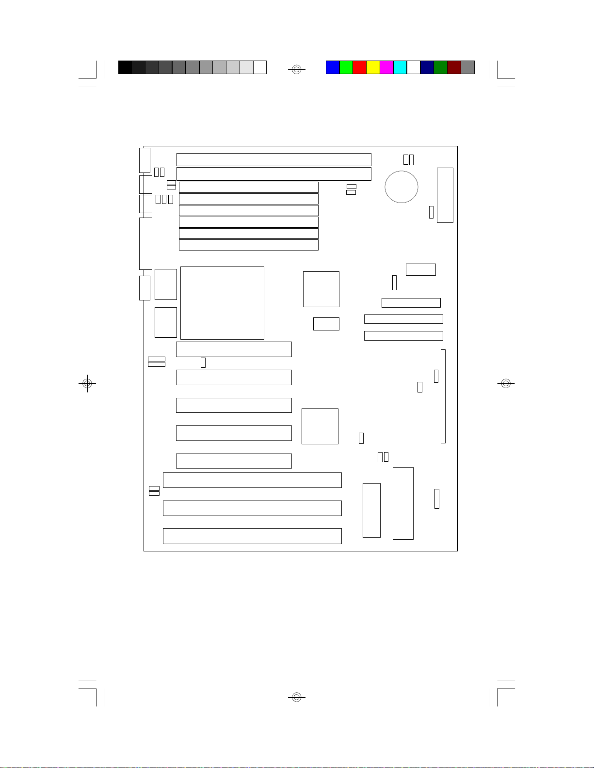
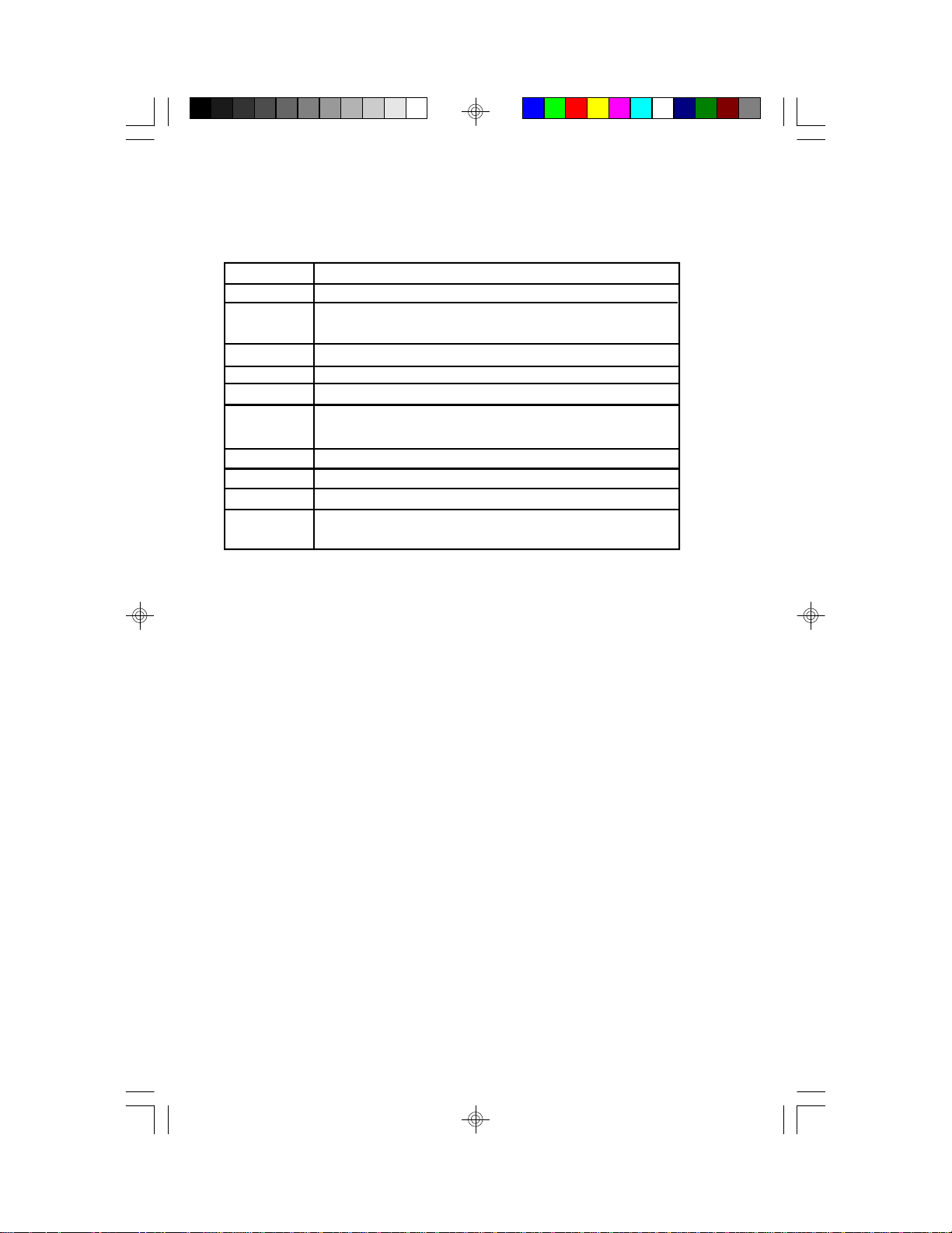
3. On Board Resource Setting
Figure 3.1 S1572 ATX Board Layout
PS/2
KB
PS/2
Mouse
JP4
JP5
Com1
JP18
JP19
JP11
JP13
JP12
Parallel Port
Com2
SRAM SRAM
USB1
pin 1
USB0
SDRAM Bank 1
SDRAM Bank 0
DRAM Bank 2
DRAM Bank 2
DRAM Bank 1
DRAM Bank 1
DRAM Bank 0
DRAM Bank 0
CPU 0
Socket 7
PCI Slot 1
JP3
PCI Slot 2
PCI Slot 3
PCI Slot 4
PCI Slot 5
Tag RAM
82371AB
82439TX
J20
1
1
JP14
pin 1
J21
JP17
JP9 JP10
pin 1
3Volt
Battery
Clk Gen.
pin 1
J23
Floppy Con.
1
Primary IDE
Secondary IDE
JP1
JP2
pin 1
J18
pin 1
pin 1
pin 1
pin 1
J2
ATX PWR CON
J8
JP15
JP16
ISA Slot 1
ISA Slot 2
ISA Slot 3
J25
KB CTR
BIOS
AMI/AWARD
8S1572-001-01 http://www.tyan.com
Page 9
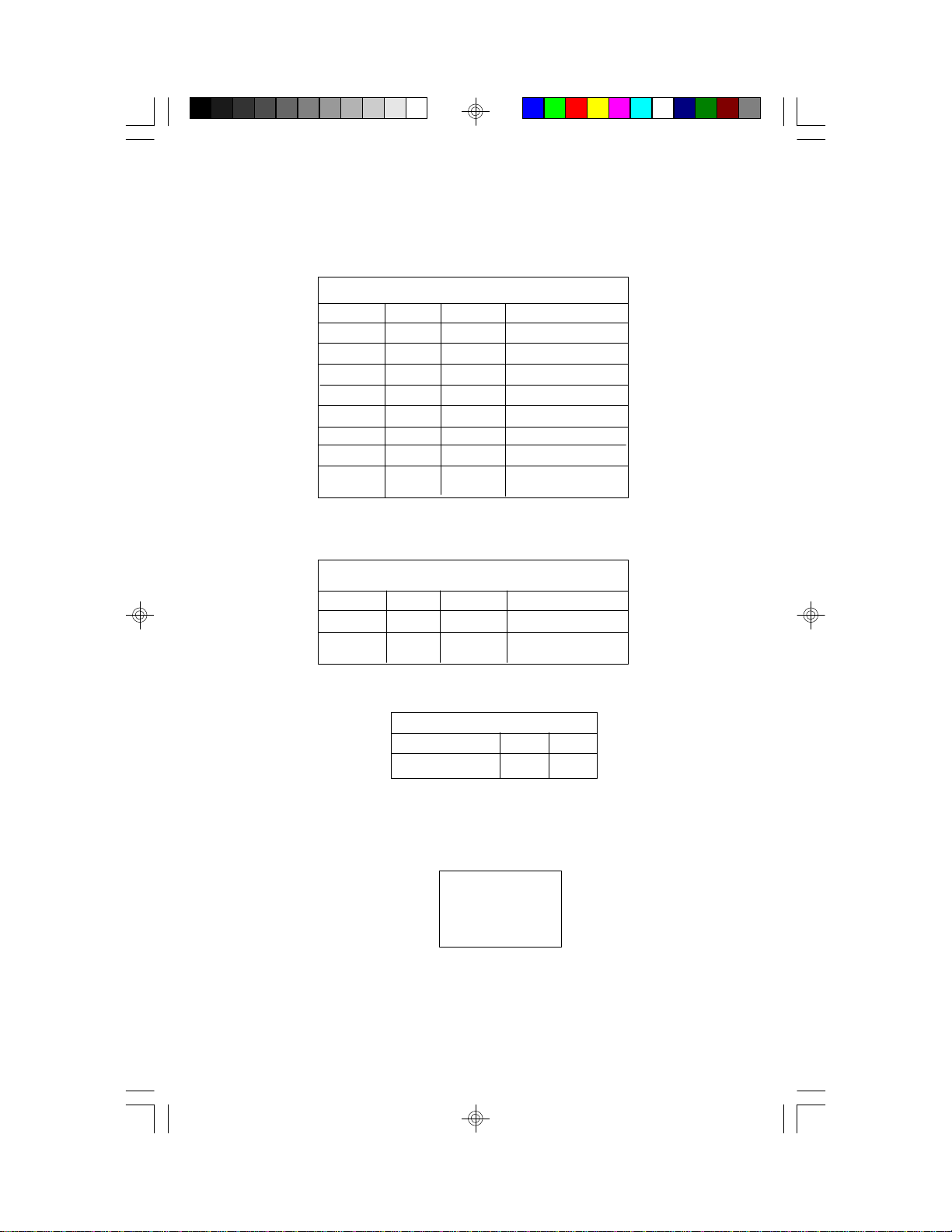
3.2 Jumper Settings
CPU Speed Settings for Pentium P54C and P55C:
JP4 JP5 JP23 CPU Speed
off off 1-2,3-4 75MHz
off off 3-4 90MHz
off off 1-2 100MHz
on off 3-4 120MHz
on off 1-2 133MHz
on on 3-4 150MHz
on on 1-2 166MHz
off on 3-4 180MHz
off on 1-2 200MHz
CPU Speed Settings for Cyrix/SGS/IBM 6x86/M1/AMD:
JP4 JP5 JP6 CPU Speed/ID
on off 1-2,3-4 100MHz/P120+
on off 3-4 120MHz/P150+
on off 1-2 133MHz/P166+
DIMM Memory Voltage Select: 3V is Default
DIMM VCC 3V 5V
JP9 1-2 2-3
JP10 1-2 2-3
Heatsink Fan Power: J18
pin1 GND
pin2 +12V
pin3 GND
9S1572-001-01 http://www.tyan.com
Page 10

BIOS Voltage Select: JP2 (Default is 5V)
BIOS 5V BIOS 12V
JP2 1-2 2-3
J8 Jumper Block:
Desc. PIN#
Soft Power 1-2
Ext SMI 3-4
IR1 8-11
Pri HDD LED 13-14
Sec HDD LED 15-16
PWR LED 18-20
Reset SW 22-23
Speaker 24-27
CPU Select: Default P54C, P55C(MMX), & Cyrix
These jumpers need not be changed. The system
will auto-detect your CPU type.
P54C,
P55C(MMX)
Cyrix
JP11 Off
JP12 Off
JP13 On
CMOS Reset: JP1(Default Battery On)
Battery On CMOS Reset
1-2 2-3
To reset CMOS, jumper JP1 on pins 2-3 for two
seconds, then jumper it back to pins 1-2.
10S1572-001-01 http://www.tyan.com
Page 11
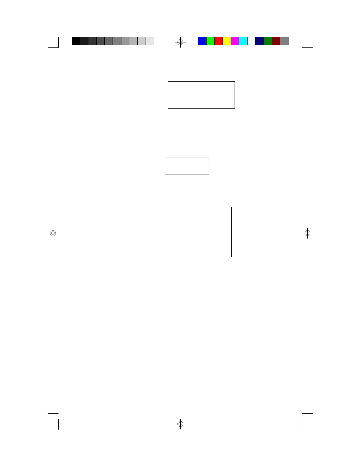
Reset Connector: J8 pin 22-23
Flash EPROM: JP2
This jumper should be left at the factory default.
Keylock Connector: J25
Pinout Assignment
22 Power Good
23 Ground
JP2 1-2
Pinout Assignments
1 Led
2 No Connect
3 Ground
4 Keylock
5 Ground
11S1572-001-01 http://www.tyan.com
Page 12

I/O Port Setting: J15 and J16
For Serial Port 1-2 1-2
For IR Port 2-3 2-3
Speaker Connector: J8 pins 24-27
Pinout Assignments
1 Speaker out
2 Ground
3 NC
4 + 5V
HDD LED: J8 pins 13-14 and pins 15-16
Pinout Assignments
13 Anode
14 Cathode
15 Anode
16 Cathode
J15 J16
Infra Red Interface: J8 pins 8-11 and J2
Pinout Assignments
1(8) Signal In
2(9) Gnd
3(10) Signal Out
4(11) VCC
12S1572-001-01 http://www.tyan.com
Page 13

3.3 CMOS RTC
CMOS RTC includes an internal battery and Real Time Clock circuit. It
provides the date and the time for the system. Normally the life span of a
RTC internal battery is 10 years. This function is built onto the Intel TX
chipset and cannot be field upgraded.
3.4 Speaker Connector Installation
S1572 provides a 4-Pin header to connect the speaker. The speaker is
connected to pins 24-27 of J8.
3.7 Hardware Reset Switch Connector Installation
The RESET switch on your cases' display panel provides users with the
HARDWARE RESET function which is the same as power on/off. The
system will do a cold start after the RESET switch is pushed by the user.
The RESET switch is a 2 pin connector and should be installed on pins
22 and 23 on J8.
3.8 Flash EPROM-Jumper JP2
The S1572 uses flash memory to store BIOS programs. It can be updated
as new versions of the BIOS becomes available. The flash utility will guide
you through the process step by step.
JP2 determines which type of EPROM is used. This jumper has been set
to match the on board BIOS chip. The factory default for the S1572 is on
pins 1-2. Depending on the type of EPROM used, some boards will have
JP2 on pins 2-3.
13S1572-001-01 http://www.tyan.com
Page 14

Refer to chapter 5 for Flash EPROM upgrade procedures.
3.9 Hardware CMOS & Password Reset
If you have been locked out of your system because you forgot your password or set the CMOS incorrectly, follow the instructions below.
a. Power off the system
b. Jumper JP1 to pins 2 and 3.
d. Wait for 2 seconds then return the jumper to pins 1 and 2.
e. Power on the system again.
By doing the above procedures, your password will be erased and the CMOS
will be reset to the BIOS default.
14S1572-001-01 http://www.tyan.com
Page 15
3.10 DRAM Installation
The S1572 uses a 64-bit data path from memory to CPU and can
accommodate up to 256MB of RAM. The mainboard supports Fast Page
Mode, and EDO (Extended Data Out) 72 pin SIMMs.
SDRAM(Synchronous) are also supported in the DIMM slots. DIMM's
must be of the unbuffered variety. All installed memory will be automatically detected so there is no need to set jumpers.
wSIMM modules must be installed in pairs.
wEach pair of SIMMs must be of the same size and type.
wThe mainboard supports 1, 2, 4, 8 and 16MBx32 SIMMs.
wSIMM bank 0, 1 and 2 can use either double or single sided SIMMs.
wTwo SIMMs or One unbuffered DIMM must be installed for the system
to POST.
wSDRAM DIMMs can be installed one at a time.
wThe mainboard supports 1, 2 and 4Mx 64 DIMM modules.
wSIMM bank 0 and DIMM bank 0 cannot be used at the same time.
SIMM bank 1 and DIMM bank 1 cannot be used at the same time.
You can use SIMM bank 0 with DIMM bank 1.
You can use SIMM bank 1 with DIMM bank 0.
wIf you use 4Mx64 DIMMs you cannot use DRAM bank 2.
wWe do not recommend using DRAM bank 2 along with DIMMs.
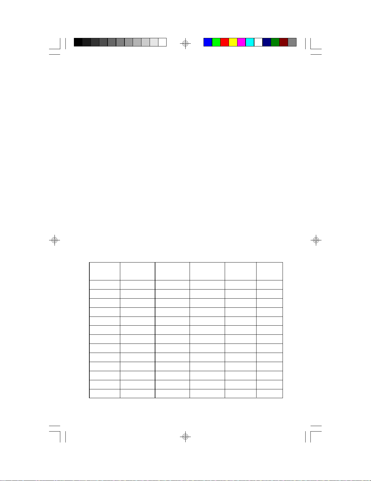
wThe following table shows some of the available memory configurations.
DRAM
Bank 0
DRAM
Bank 1
DRAM
Bank 2
SDRAM
Bank 0
SDRAM
Bank 1
Total
4MB x2 none none none none 8MB
none none none 8MB x1 none 8MB
none none none 16MB x1 none 16MB
8MB x2 none none none none 16MB
4MB x2 4MB x2 4MB x2 none none 24MB
16MB x2 none none none none 32MB
none 8MB x2 none 16MB x1 none 32MB
32MB x2 none none none none 64MB
none none none none 64MB x1 64MB
none none none 32MB x1 64MB x1 96MB
none none none 64MB x1 64MB x1 128MB
64MB x2 none none none 64MB x1 192MB
64MB x2 64MB x2 64MB x2 none none 256MB
15S1572-001-01 http://www.tyan.com
Page 16

3.11 CPU Installation
Several types of CPUs (75 thru 200MHz) can be used on S1572.
Please refer to section 3.2 for the correct CPU jumper settings for your
board.
w The CPU is a sensitive electronic component and it can be easily
damaged by static electricity. Do not touch the CPU pins with your
fingers.
w When installing the CPU into the socket, match the CPU pins to the
socket pins.
w Before the CPU is installed, the mainboard must be placed on a flat
plane. You should be able to insert the CPU with minimal pressure.
Do not push down hard, use firm pressure.
w A cooling fan and heat sink assembly is required to protect the
CPU from being damaged.
1. Make sure the ZIF socket lever is up. To raise the lever, pull it out
to the side a little and raise it as far as it will go. The top plate will
slide back.
2. Align the CPU and socket Pin 1 corners. The pins on the bottom
should align with the rows of holes in the socket.
3. Insert the CPU in the socket. It should insert easily. If it does
not, adjust the position of the lever a little.
4. Press the lever down. The top plate will slide forward. You will
feel some resistance as the pressure starts to secure the CPU in
the socket. This is normal and will not damage the CPU.
The lever should snap into place at the side of the socket.
16S1572-001-01 http://www.tyan.com
Page 17

3.12 Upgrading Cache Memory
The S1572's 512kb of on-board pipelined burst SRAM and cannot be
field upgraded. The TX chipset can cache a maximium of 64MB of
RAM.
3.13 Peripheral Device Installation
After all the jumpers on the mainboard have been set, then it can be mounted
into the case. Proceed to install the display card and any other peripheral
devices.
If a PCI-Bus interface card is to be installed in the system, any one of the
five PCI-Bus slots can support either a Master or a Slave device.
After installing the peripheral controllers, the user should check everything
again, and prepare to power on the system.
17S1572-001-01 http://www.tyan.com
Page 18

4. BIOS Configuration
Award's BIOS has a built in setup program that allows the user to modify
the basic system configuration. This type of information is stored in the
battery-backed CMOS NVRAM. Entering incorrect information or for-
getting your password can lock you out of your system.(refer to 3.9
for resetting of CMOS)
4.1. Entering Setup
Power ON the computer and press <Del> immediately and you will enter
Setup. The other way to enter setup is to power on the computer, when the
below message appears briefly at the bottom of the screen during the POST
(Power On Self Test), press <Del> key or simultaneously press <Ctrl>,
<Alt>, and <Esc> keys.
* TO ENTER SETUP BEFORE BOOT PRESS CTRL-ALT ESC OR DEL KEY
If the message disappears before you respond and you wish to enter Setup,
restart the system by turning it OFF then ON or by pressing "Reset" on the
system case. You may also restart by simultaneously pressing <Ctrl>, <Alt>,
and <Del> keys. If you do not press the keys at the correct time, the system
will not boot and an error message will appear on the screen. You will be
asked to;
* PRESS F1 TO CONTINUE, CTRL-ALT-ESC OR DEL TO
ENTER SETUP.
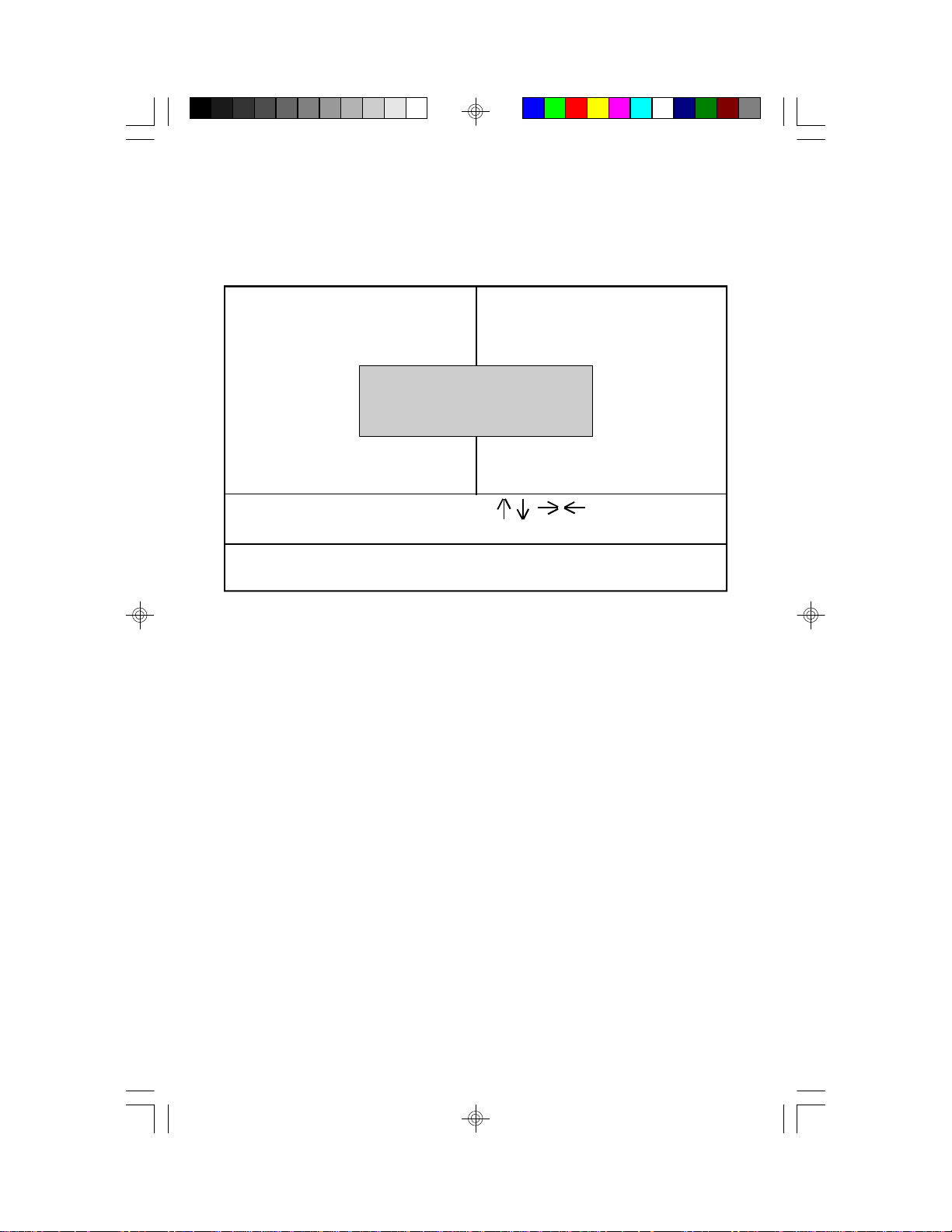
Figure 4.1 will appear on the sceen. The Main Menu allows you to select
from the 8 setup functions and 2 exit choices. Use the arrow keys to select
among the items and press <Enter> to accept or enter each sub-menu.
18S1572-001-01 http://www.tyan.com
Page 19
4.2. Control Keys
PgUp key Increases the numeric value or make changes
PgDn key Decreases the numeric value or make changes
F1 key General help, only for Status Page Setup menu
and Option Page Setup Menu
F2 key Change color from a total of 16 colors
F3 key Calendar, only for Status Page Setup Menu
F4 key Reserved
F5 key Restore the previous CMOS value, only for Option
Page Setup Menu
F6 key Load defaults
F8 key Reserved
F9 key Reserved
F10 key Save all CMOS changes, only for Main Menu
19S1572-001-01 http://www.tyan.com
Page 20

4.3. Getting Help
4.3.1. Main Menu
The on-line description of the highlighted setup function is displayed at the
bottom of the screen.
4.3.2. Setup Page menu/Option Page Setup Menu
Press F1 to pop up a small help window that describes the appropriate keys
to use and the possible selections for the highlighted items. To exit the Help
Window, press <Esc>.
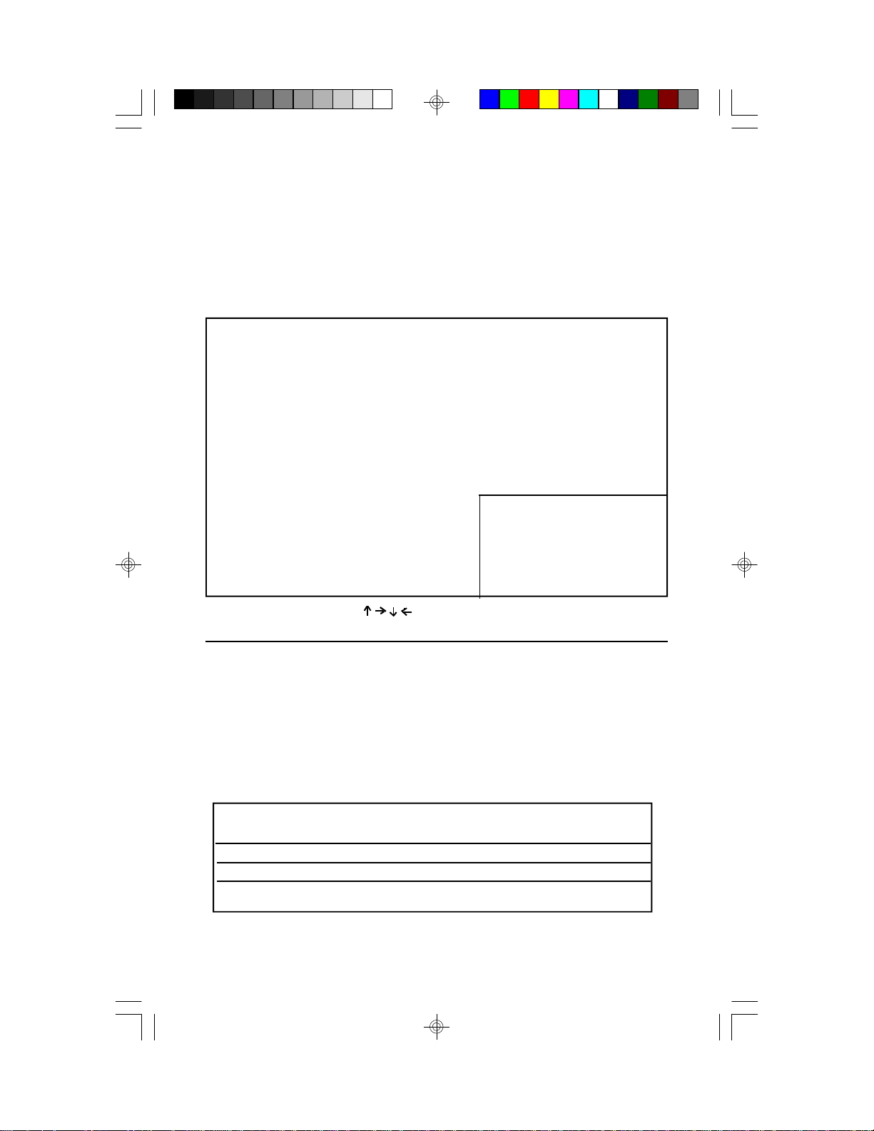
4.4. The Main Menu
Once you enter the Award BIOS CMOS Setup Utility, the Main Menu
(Figure 4.1) will appear on the screen. The Main Menu allows you to
select from the eight setup functions and 2 exit choices. Use the arrow
keys to select among the items and press <Enter> to accept or enter the
sub-menu.
Figure 4.1: Main Menu
ROM ISA BIOS (2A59CT51)
CMOS SETUP UTILITY
AWARD SOFTWARE, INC.
STANDARD CMOS SETUP INTEGRATED PERIPHERALS
BIOS FEATURES SETUP SUPERVISOR PASSWORD
CHIPSET FEATURES SETUP USER PASSWORD
POWER MANAGEMENT IDE HDD AUTO DETECT
PNP/PCI CONFIGURATION SAVE AND EXIT
LOAD BIOS DEFAULTS EXIT WITHOUT SAVING
ESC : Save & Exit Setup
F10 : Quit
:Select Item
(Shift)F2 :Change Color
Time, Date, Hard Disk Type,.....
20S1572-001-01 http://www.tyan.com
Page 21

w Standard CMOS setup
This setup page includes all the items in a standard compatible BIOS.
w BIOS features setup
This setup page includes all of the enhanced features of Award's BIOS.
w Chipset features setup
This setup page includes all the items of the 430TX chipset features.
w Power Management setup
Change, set, or disable system power management options.
w PNP/PCI Configuration
This setup page allows you to modify the configuration of PCI slot
parameters.
w Load setup defaults
BIOS defaults indicate the most appropriate values of each system param eter for your system.
w Supervisor/User Password
Change, set, or disable password. It allows you to limit access to the
system and Setup.
w Integrated Peripherals
This option lets you enable or disable on board FDD, HDD,
and I/O options.
w IDE HDD auto detection
Automatically configure hard disk parameters.
w Save and exit setup
Save changes to CMOS and exit setup.
w Exit without saving
Abandon all CMOS changes and exit setup.
21S1572-001-01 http://www.tyan.com
Page 22
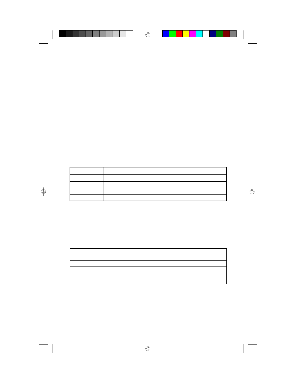
4.5. Standard CMOS Setup Menu
The items in Standard CMOS Setup Menu (Figure 4.2) are divided into 9
categories. Each category includes one or more setup items. Use the
arrows to highlight the item and use the <PgUp> or <PgDn> keys to
select the value you want for each item.
Figure 4.2: Standard CMOS Setup Menu
ROM ISA BIOS (2A59CT51)
STANDARD CMOS SETUP
AWARD SOFTWARE, INC.
Date (mm:dd:yy) : Tue, Dec 7 1995
Time (hh:mm:ss) : 18 : 01 : 38
Type Size CYLS. HEADS. PRECOMP. LANDZONE SECTORS
Primary Master : none 0mb 0 0 0 0 0
Primary Slave: none 0mb 0 0 0 0 0
Secondary Master: none 0mb 0 0 0 0 0
Secondary Slave: none 0mb 0 0 0 0 0
Drive A : 1.44 M, 3.5 in.
Drive B : 1.2 M, 5.25 in.
Video : EGA/VGA
Halt On : All errors
Base Memory: 640 K
Extended Memory: 7168 K
Expanded Memory: 0 K
Other Memory: 384 K
Total Memory: 8192 K
ESC: Quit : Select Item PU/PD/+/-: Modify
F1: Help (Shift)F2: Change Color F3: Toggle Calendar
w Date
The date format is <month>, <day>, <year>. Press <F3> to show the
calendar.
w Time
The time format is <hours>, <minutes>, <seconds>. The time is calcu lated based on the 24-hour military-time clock. For example 1 p.m. is
13:00:00.
Day The day, from Sun to Sat, Determined by the BIOS date,
month and year entries.
Date The date, from 1 to 31 (or maximum allowed in a month)
Month The month, Jan to Dec.
Year The year, from 1900 to 2099
22S1572-001-01 http://www.tyan.com
Page 23
w Primary/Secondary Drive Type
This category identifies the types of hard disk drives that have been installed in the computer. There are 46 predefined types and a user definable
type.
Press PgUp or PgDn to select a numbered hard disk type or type a number
and press <Enter>. Note that the specifications of your drive must match
with the drive table. The hard disk will not work properly if you enter
improper information for this category. If your hard disk type is not listed,
you can Type User to define your own drive manually.
If you select Type User, you will be asked to enter the following info. Enter
the paramters directly from the keyboard and press <Enter>. The hard disk
information should be provided in the documentation from the hard disk
vendor or the system manufacturer.
CYLS number of cylinders
HEADS number of heads
PRECOMP written precom
LANDZONE landing zone
SECTORS number of sectors
If a hard disk has not been installed or you have a CD-ROM/Tape drive
connected to an IDE channel, select NONE and press <Enter>.
w Drive A type/Drive B type
This category identifies the types of floppy disk drive A or B, that
have been installed in your computer.
None No floppy drive installed
360K, 5.25 in. 5-1/4 inch PC-type standard drive ; 360 kilobyte capacity
1.2M ,5.25 in. 5-1/4 inch AT-type high-de nsity driv e; 1.2 me gabyte capacity
720K, 3.5 in. 3-1/2 inch double-side d drive ; 720 kilobyte capacity
1.44M, 3.5 in. 3-1/2 inch double-sided driv e ; 1.44 me gabyte capacity
2.88M, 3.5 in. 3-1/2 inch double-sided driv e ; 2.88 me gabyte capacity
23S1572-001-01 http://www.tyan.com
Page 24
w Video
This category detects the type of graphics adapter used for the primary
display system. It must match your video display card and monitor. Although secondary monitors are supported, you do not have to select that
type in setup.
EGA/VGA Enhanced Graphics Adapter/Video Graphics Array.
For VGA,SVGA, or PGA monitor adapters.
CGA 40 Color Graphics Adapter, power up in 40 column mode.
CGA 80 Color Graphics Adapter, power up in 80 column mode.
Mono Monochrome adapter, includes hi-res monochrome.
w Halt On
The category determines whether the computer will stop if an error is
detected during power up.
No errors Whenever the BIOS has detected a non-fatal error, the
system will be stopped and you will be promted.
All errors The system boot will not be stopped for any errors that
are detected.
All, but Keyboard The system boot will not stop for a keyboard error;it
will stop for all other errors.
All, but Diskette The system boot will not stop for disk errors; it will
stop for all other errors.
All, but Disk/Key The system boot will not stop for a keyboard or disk
error; it will stop for all other errors.
w Memory
The category is for display-only and it is determined by POST (Power On
Self Test) of the BIOS.
Base Memory
The POST of the BIOS will determine the amount of
base (or conventional) memory installed in the system.
The value of the base memory is typically 640K.
Extended Memory
The BIOS determines how much extended memory is
present during the POST. This is the amount of
memory located above 1MB in the CPU's memory
address map.
24S1572-001-01 http://www.tyan.com
Page 25
Expanded Memory
Expanded Memory (EMS) defines a 64K page frame in
the area between 640K and 1Mb containing four 16K pages
that are windows into the EMS memory. Programs issue
requests to the EMS manager to switch the page to any
part of EMS memory. Extended memory can be converted
to emulate EMS by using a memory manager such as
EMM386 that ships with Windows and DOS.
Other Memory
This refers to memory located in the 640K to 1024K ad-
dress space. This memory can be used for different
applications. DOS uses this area to load device drivers to
keep as much conventional memory free for application
programs as possible.
4.6. BIOS FEATURES SETUP
ROM ISA BIOS
BIOS FEATURES SETUP
AWARD SOFTWARE, INC.
Virus Warning :Enabled
CPU Internal Cache :Enabled
External Cache :Enabled
Boot Sequence :A,C
Swap Floppy Drive :Disabled
Boot Up Floppy Seek :Enabled
Boot Up NumLock Status :On
Typematic Rate Setting :Disabled
Typematic Rate (Chars/sec) :6
Typematic Delay (msec) :250
Security Option :Setup
PS/2 Mouse Function :Enabled
PCI/VGA Palette Snooping :Disabled
OS select for DRAM >64MB:non-OS/2
Video BIOS Shadow :Enabled
C8000-CBFFF Shadow :Disabled
CC000-CFFFF Shadow :Disabled
D0000-D3FFF Shadow :Disabled
D4000-D7FFF Shadow :Disabled
D8000-DBFFF Shadow :Disabled
DC000-DFFFF Shadow :Disabled
ESC :Quit :Select Item
F1 :Help PU/PD/+/- :Modify
F5 :Old Values (Shift)F2 :Color
F6 :Load BIOS Defaults
F7 :Load Setup Defaults
25S1572-001-01 http://www.tyan.com
Page 26

w Virus warning
d
This category flashes on screen. During and after the system boot up,
any attempt to write to the boot sector or the partition table of the hard
disk drive will halt the system and the following error message will
appear. In the meantime, you can run an anti-virus program to locate the
problem. Default value is Enabled.
"Attempting to write to boot sector, continue? Y/N"
Enabled Activate automatically when the system boots up causing a warning
me ssage to appe ar when anything attemps to acce ss the boot sector or har
disk partition table.
Disabled No warning me ssage to appear when anything attemps to access the boot
sector or hard disk partition table .
w CPU Internal Cache/External Cache
These two categories speed up the memory access. However, it de pends on the CPU/Chipset design. Default value is Enabled.
Enabled Enables the cache
Disabled Disable s the cache
w Boot Sequence
This category determines which drive the computer searches first for the
disk operating system (i.e. DOS). Default value is A,C.
A,C Syste m will f irst search f or floppy disk drive then hard disk drive.
C,A Syste m will f irst search f or hard disk drive then floppy disk drive
w Swap Floppy Drive
Default value is Disabled
Enabled Floppy A & B will be swapped under DOS
Disable Floppy A & B will be normal definition.
26S1572-001-01 http://www.tyan.com
Page 27
w Boot Up Floppy Seek
During POST, the BIOS will determine if the floppy disk drive installed is
40 or 80 tracks. 360K type is 40 tracks while 720K, 1.2M and 1.44M
are all 80 tracks. Default value is Enabled
Enabled BIOS searches for floppy disk drive to determine if it is 40 or 80
tracks. Note that the BIOS cannot tell from 720k, 1.2M or 1.44M
drive type as they are all 80 tracks
Disabled BIOS will not search for the type of floppy disk drive by track
number. Note that there will not be any warning messages if the
drive installed is 360K
w Boot Up NumLock Status
Default value is On
On Keypad is number keys
Off Ke ypad is arrow keys
w Gate A20 Option
Gate A20 controls the ability to access memory addresses above 1 MB
by enabling (Fast) or disabling (Normal) access to the processor.
Default value is Fast
w Typematic Rate Setting, Typematic Rate (char/sec), and
Typematic Delay.
Typematic Rate Setting enables or disables the following two options.
TheTypematic Rate (6, 8, 10, 12, 15, 20, 24, or 30 characters per second)
and Typematic Rate Delay (250, 500, 750, or 1000 milliseconds) control
the speed at which the keystroke is repeated. The selected character is
displayed when a key is held down after a delay set by the Typematic
Rate Delay. It then repeats at a rate set by the Typematic Rate.
27S1572-001-01 http://www.tyan.com
Page 28

w Security Option
This category allows you to limit access to the system setup, or just
setup. Default value is Setup
S ystem The system will not boot and access to Setup will be denied if the correct
password is not e ntered at the prompt
Setup The syste m will boot, but access to setup will be denied if the password is
not entered at the prompt
w Video BIOS Shadow
It determines whether Video BIOS will be copied to RAM, however, it
is an optional chipset design. Default is Enabled.
4.7 Chipset Features Setup
This screen controls the settings for the board's chip set. The controls for
this screen are the same as the previous screen.
The Chipset Features Screen
ROM ISA BIOS
CHIPSET SETUP UTILITY
AWARD SOFTWARE, INC.
Auto Configuration :Enabled
DRAM Timing :70ns
DRAM Leadoff Timing :10/6/3
DRAM Readburst (EDO/FP) :x222/x333
DRAM Write Burst Timing :x333
Fast EDO Path Select :Disabled
Refresh RAS# Assertion :5/Clks
Fast RAS to CAS delay :2
DRAM Page Idle Timer :8Clks
DRAM Enhanced Paging :Enabled
Fast MA to RAS# delay :1 Clks
SDRAM(cas lat/ras to cas) :2/2
SDRAM Speculative Read :Disabled
System BIOS Cacheable :Enabled
Video BIOS Cacheable :Enabled
8 bit I/O Recovery Time :1
16 bit I/O Recover Time :1
Memory Hole at 15M/16M :Disabled
PCI Passive Release :Enabled
PCI Delayed Transaction :Enabled
Pipline Cache Timing :Faster
Mem Drive Strength(ma/ras) :2/2
DRAM Refresh :15.6us
More Information on these settings
can be found at Tyan's web site.
http://www.tyan.com
ESC :Quit :Select Item
F1 :Help PU/PD/+/- :Modify
F5 :Old Values (Shift)F2 :Color
F6 :Load BIOS Defaults
F7 :Load Setup Defaults
28S1572-001-01 http://www.tyan.com
Page 29

4.7.1 Power Management Setup
ROM ISA BIOS
POWER MANAGEMENT SETUP
Power Management :Disabled Reload Global Timer Events
PM Control By APM :No IRQ (3-7, 9-15), NMI Disable
Video Off Method :Blank Screen Primary IDE 0 Disable
Video Off After :N/A Primary IDE 1 Disable
Doze Mode :Disabled Secondary IDE 0 Disable
Standby Mode :Disabled Secondary IDE 1 Disable
Suspend Mode :Disabled Floppy Disk Disable
HDD Power Down :Disabled Serial Port Disable
Throttle Duty Cycle :62.5% Parallel Port Disable
ZZ Active Monitor :Disable
IRQ8 Clock Event :Disable
AWARD SOFTWARE, INC
wPower Management
Options are disabled, user defined, Min saving, and Max saving.
wPM Control by APM
Options are "Yes" and "No". When set for "No", system BIOS will
ignore APM when power managing the system. If set on "Yes" the
system BIOS will wait for APM's prompt before it enters any PM
mode, e.g. Doze, Standby or Suspend.
wVideo Off Method
The "Blank Screen" option will let the system BIOS blanks the screen
when disabling video. V/H SYNC+Blank will let the BIOS turn off the
V-SYNC and H-SYNC signals from the VGA card to the monitor.
29S1572-001-01 http://www.tyan.com
Page 30

w Doze Mode
Defines the continous idle time before the system enters Doze mode.
wStandby Mode
Defines the continous idle time before the system enters Standby mode.
wReload Global Timer Events
Defines the the activities that can cause the PM timers to reload. (Breaking out of PM Mode)
30S1572-001-01 http://www.tyan.com
Page 31
4.8 PCI Slot Configuration
PCI SLOT CONFIGURATION
AWARD SOFTWARE, INC.
ROM ISA BIOS
Resource Controlled by :Manual
Reset Configuration :Disabled
IRQ3 assigned to :legacy ISA
IRQ4 assigned to :legacy ISA
IRQ5 assigned to :PCI/PnP
IRQ7 assigned to :legacy ISA
IRQ9 assigned to :PCI/PnP
IRQ10 assigned to :PCI/PnP
IRQ11 assigned to :PCI/PnP
IRQ12 assigned to :PCI/PnP
IRQ14 assigned to :legacy ISA
IRQ15 assigned to :legacy ISA
DMA0 assigned to :PCI/PnP
DMA1 assigned to :PCI/PnP
DMA3 assigned to :PCI/PnP
DMA5 assigned to :PCI/PnP
DMA6 assigned to :PCI/PnP
DMA7 assigned to :PCI/PnP
w PCI Slot 1/Slot 2/Slot 3/Slot 4/Slot 5 INT#
w For Default Setting.
Connect to PCI System INT#
PCI Slot1 INTA INTA
PCI Slot1 INTB INTB
PCI Slot1 INTC INTC
PCI Slot1 INTD INTD
PCI Slot2 INTA INTB
PCI Slot2 INTB INTC
PCI Slot2 INTC INTD
PCI Slot2 INTD INTA
PCI Slot3 INTA INTC
PCI Slot3 INTB INTD
PCI Slot3 INTC INTA
PCI Slot3 INTD INTB
PCI Slot4 INTA INTD
PCI Slot4 INTB INTA
PCI Slot4 INTC INTB
PCI Slot4 INTD INTC
PCI Slot5 INTA INTA
PCI Slot5 INTB INTB
PCI Slot5 INTC INTC
PCI Slot5 INTD INTD
PCI IRQ Activated By: Level
PCI IDE IRQ Map To: Auto
Primary IDE INT#: A
Secondary IDE INT#: B
ESC: Quit :Select Item
F1 : Help PU/PD/+/- :Modify
F5 : Old Values (Shift)F2 :Color
F6 : Load BIOS Defaults
F7 : Load Setup Defaults
31S1572-001-01 http://www.tyan.com
Page 32

wResources Controlled By
The Award Plug and Play BIOS can automatically configure all the boot
and Plug and Play compatible devices. If you select Auto, all the
interrupt request and DMA assignment fields disappear, as the BIOS
automatically assigns them.
wIRQ n assigned to
When resources are controlled manually, assign each system interrupt
as one of the following types, depending on the type of device using
the interrupt.
Legacy ISA
Devices compliant with the original PC AT bus specification.
PCI/ISA PnP
Devices compliant with the Plug and Play standard, whether designed
for the PCI or ISA bus architecture.
wPCI IRQ Activated By:
Select the PCI IRQ Active scheme either LEVEL or EDGE.
Default value is LEVEL.
wPCI IDE IRQ Map To:
Select the IDE IRQ Map to ISA IRQ#.
wPrimary IDE INT#
Select the PCI INT# that the Primary IDE controller will use.
Default value is A.
wSecondary IDE INT#
Select the PCI INT# that the Secondary IDE controller will use.
Default value is B
32S1572-001-01 http://www.tyan.com
Page 33

4.9 Integrated Peripherals
Integrated Peripherals
Award Software, Inc.
IDE HDD Block Mode :Enabled
IDE Primary Master PIO :Auto
IDE Primary Slave PIO :Auto
IDE Secondary Master PIO :Auto
IDE Secondary Slave PIO :Auto
IDE Primary Master UDMA :Auto
IDE Primary Slave UDMA :Auto
IDE Secondary Master UDMA :Auto
IDE Secondary Slave UDMA :Auto
On-Chip Primary PCI-IDE :Enable
On-Chip Secondary PCI-IDE :Enable
USB Keyboard Support :Disable
USB Latency Time (PCI CLK):32
On-Board FDC Controller :Enable
On-Board UART 1 :Com1/3F8
On-Board UART 2 :Com2/2F8
On-Board UART 2 :Standard
On-Board Parallel Port :378/IRQ7
Parallel Port Mode :Normal
The Settings in the Integrated Peripherals section lets the user enable or
disable on-board devices. You can also configure the I/O and IRQ
settings of the on-board serial and parallel ports.
33S1572-001-01 http://www.tyan.com
Page 34
4.10. LOAD SETUP DEFAULTS
ROM ISA BIOS
CMOS SETUP UTILITY
AWARD SOFTWARE INC.
STANDARD CMOS SETUP PASSWORD SETTING
BIOS FEATURES SETUP IDE HDD AUTO DETECTION
CHIPSET FEATURES SETUP DAVE & EXIT SETUP
PCI SLOT configuration EXIT WITH OUT SAVING
LOAD SETUP DEFAULTS
ESC : Save & Exit Setup
F10 : Quit
Load SETUP Defaults except standard CMOS SETUP
Load Setup Defaults (Y/N)? N
:Select Item
(Shift)F2 :Change Color
w Load SETUP defaults
To load SETUP default values to CMOS NVRAM, enter "Y". If not,
enter "N"
w If any problem has occurred, loading the SETUP DEFAULTSis
recommended.
4.11. PASSWORD SETTING
When you select this function, the following message will appear at the
center of the screen to assist you in creating a password.
ENTER PASSWORD
34S1572-001-01 http://www.tyan.com
Page 35
ROM ISA BIOS
CMOS SETUP UTILITY
AWARD SOFTWARE, INC.
STANDARD CMOS SETUP PASSWORD SETTING
BIOS FEATURES SETUP IDE HDD AUTO DETECTION
CHIPSET FEATURES SETUP DAVE & EXIT SETUP
PCI SLOT CONFIGURATION EXIT WITH OUT SAVING
LOAD SETUP DEFAULTS
ESC : Save & Exit Setup
F10 : Quit
Enter Password
:Select Item
(Shift)F2 :Change Color
Change/Set/Disable Password
Type the password, up to eight characters, and press <Enter>. The
password typed now will clear the previously entered password from
CMOS memory. You will be asked to confirm the password. Type the
password again and press <Enter>. You may also just press <Esc> to
abort the selection and not enter a password.
To disable the password, just press <Enter> when you are prompted to
enter a password. A message will confirm that the password has been
disabled, the system will boot and you can enter Setup freely.
PASSWORD DISABLED
If you select System at Security Option of BIOS Features Setup Menu, you
will be prompted for the password every time the system is rebooted or any
time you try to enter setup. If you select Setup at Security Option of BIOS
Features Setup Menu, you will be prompted only when you try to enter
setup.
35S1572-001-01 http://www.tyan.com
Page 36

4.12. IDE HDD AUTO DETECTION
ROM ISA BIOS
CMOS SETUP UTILITY
AWARD SOFTWARE, INC.
CYLS. HEAD PRECOMP LANZONE SECTORS
Drive C: (202 Mb) 989 12 65535 989 35
Do you want to accept this as drive C (Y/N)?
Esc:Skip
Type "Y" to accept the H.D.D parameter reported by BIOS. Type "N" to keep the old
H.D.D parameter info.
4.13. SAVE & EXIT SETUP
ROM ISA BIOS
CMOS SETUP UTILITY
AWARD SOFTWARE, INC.
STANDARD CMOS SETUP PASSWORD SETTING
BIOS FEATURES SETUP IDE HDD AUTO DETECTION
CHIPSET FEATURES SETUP DAVE & EXIT SETUP
PCI SLOT CONFIGURATION EXIT WITH OUT SAVING
Save to CMOS and EXIT (Y/N)? N
LOAD SETUP DEFAULTS
ESC : Save & Exit Setup
F10 : Quit
(Shift)F2 :Change Color
:Select Item
Time, Date, Hard Disk Type,.....
Type "Y" and you will quit the Setup Utility and save the user setup values to RTC CMOS
NVRAM. Type "N" to return to Setup Utility.
36S1572-001-01 http://www.tyan.com
Page 37

5.0 Flash Writer Utility
You can upgrade the BIOS of your mainboard by using a "Flash
Memory Writer"(FMW) utility. This utility can be downloaded from the
factory's BBS(Consult your system vendor for the phone #). The
system BIOS is stored on a 'flash' EPROM ROM chip on the
mainboard which can be erased and reprogrammed by the FMW.
The following three files make up the FMW.
AWDFLASH.EXE -The Flash Memory Writer utility for
Award to Award upgrade.
AMIFLASH.COM -The Flash Memory Writer utility for
AMI to AMI upgrade.
README -A text file of instructions
*S72AWXX.BIN -XX-A 2-digit version number.
The Flash memory writer records (or ‘programs’) a new BIOS
onto the flash memory chip. You cannot upgrade an Award
BIOS to a AMI BIOS or a AMI BIOS to an Award BIOS.
*This file name is subject to change and can have either a "bin" or a
"rom" extention.
Note
You should ALWAYS clear your CMOS after flashing a BIOS.
This will clear out any stray settings from your old BIOS which may
have been carried over from the flashing process. Most problems
encountered after flashing a BIOS will be solved by this simple
procedure.
37S1572-001-01 http://www.tyan.com
Page 38

To reprogram the System BIOS, you must first do the following:
1. Check jumper JP2.(Default pins 1-2)
The S1572 uses a 5V Flash EPROM so jumper JP2
should be left in the default postion on pins 1 and 2. This
jumper should never be moved.
2. Make sure the CPU is running in ‘real mode’.
FMW will not run if the CPU is operating in a protected or
virtual mode. This means that you can not run it with Windows
running or with any memory manager software. You must
disable any memory manager first. The easiest way to do this
is to:
a. Boot your system from a bootable floppy disk with no
CONFIG.SYS or AUTOEXEC.BAT files, and then run Flash
Memory Writer from a backup copy of your support disk. You
can make your back-up floppy bootable when you format it, and
use one disk for both purposes.
b. If you are using MS-DOS 6.x, you can use the feature that
allows you to bypass the CONFIG.SYS and AUTOEXEC.BAT
file. You do this while pressing <F5> while the “Starting MS-
DOS...” line is on the screen.
There are other ways to accomplish the same result. The main
point is to make sure no memory managers are running. If you
are not sure, try running FMW. If it runs, then you have succeeded. If it displays a warning message about the CPU
mode, you will have to try again.
38S1572-001-01 http://www.tyan.com
Page 39

Once you have satisfied the two requirements mentioned above,
you can run FMW. You can copy the contents of the “Flash”
directory to your hard drive, or you can run the utility from a
backupof the support floppy disk. Make sure the new BIOS file
is in thesame directory as the FMW utility.
To run FMW, change to the “Flash” directory if you are not already in it. Type “Awdflash” at the DOS command line and press
the <Enter> key. The following screen will appear.
5.1 The Flash Memory Writer Utility Screen (Award)
FLASH MEMORY WRITER V3.0
Copyright (C) 1993, AWARD Software Inc.,
For VX/HX-2A59CT51 Date:4/13/95
File Name to Program:
Error Message:
Type in the whole file name, e.g. A61AW10.BIN and confirm
that you want to program the BIOS. The utility will then ‘Blank’,
‘Erase’, and then ‘Program’ the flash memory on the mainboard with the
new BIOS file. You should choose “yes” to save the original system
BIOS to a floppy diskette before you program the new BIOS. This
leaves you with a backup of your original BIOS in case you need to reinstall it. This option is highly recommended. If you can not sucessfully
program the BIOS file for whatever reason, re-install you original BIOS
from the backup file. Always reset the CMOS with jumper JP1 after
flashing to a new BIOS.
Warning: If you do not successfully install a complete BIOS file
in the flash memory on the Mainboard, your system may not be able to
boot. If this happens, it will require service by your system vendor.
Follow the requirements and instructions in this section precisely to avoid
inconvenience.
39S1572-001-01 http://www.tyan.com
Page 40

6.0 System Resource
6.1. TIMER & DMA CHANNEL MAP
TIMER MAP: TIMER Channel-0 system timer interrupt
TIMER Channel-1 DRAM REFRESH request
TIMER Channel-2 SPEAKER tone generator
DMA CHANNELS: DMA Channel-0 Available
DMA Channel-1 Available
DMA Channel-2 FLOPPY DISK adapter
DMA Channel-3 Available
DMA Channel-4 Cascade for DMA controller 1
DMA Channel-5 Available
DMA Channel-6 Available
DMA Channel-7 Available
6.2 INTERRUPT MAP
NMI: Parity check error
IRQ (H/W) 0 System TIMER interrupt from TIMER-0
1 KEYBOARD output buffer full
2 Cascade for IRQ 9-15
3 SERIAL port 2
4 SERIAL port 1
5 PARALLEL port 2
6 FLOPPY DISK adapter
7 PARALLEL port 1
8 RTC clock
9 Available
10 Available
11 Available
12 PS/2 Mouse
13 MATH co-processor
14 Primary IDE
15 Secondary IDE
40S1572-001-01 http://www.tyan.com
 Loading...