

Page 1

Trinity KT400 S2495 User’
s Manual
S2495
Tri nity KT400
///
Revision 1.02
Copyright © TYAN Computer Corporation, 2003. All rights reserved. No part of this manual
may be reproduced or translated without prior written consent from TYAN Computer Corp.
All registered and unregistered trademarks and company names contained in this manual are
property of their respective owners including, but not limited to the following.
TYAN, Trinity, KT400 and S2495 are trademarks of TYAN Computer Corporation.
AMD, Athlon and Duron are trademarks of Advanced Micro Devices, Inc.
VIA, KT400, are trademarks of VIA Technologies, Inc.
Silicon Image is a trademark of Silicon Image, Inc.
High Point is a trademark of HighPoint Technologies, Inc.
Award, AwardBIOS are trademarks of Award Software Incorporated.
Microsoft and Windows are trademarks of Microsoft Corporation.
IBM, PC, AT and PS/2 are trademarks of IBM Corporation.
Winbond is a trademark of Winbond Electronics Corporation.
Sony/Philips Digital Interface (SPDIF) is a trademark of Sony Corporation and Philips
Electronics.
Portable Document Format (PDF) is a trademark of Adobe Corporation.
Information contained in this document is furnished by TYAN Computer Corporation and has
been reviewed for accuracy and reliability prior to printing. TYAN assumes no liability
whatsoever, and disclaims any express or implied warranty, relating to sale and/or use of
TYAN products including liability or warranties relating to fitness for a particular purpose or
merchantability. TYAN retains the right to make changes to product descriptions and/or
specifications at any time, without notice. In no event will TYAN be held liable for any direct or
indirect, incidental or consequential damage, loss of use, loss of data or other malady resulting
from errors or inaccuracies of information contained in this document.
http://www.tyan.com
i
Page 2

Trinity KT400 S2495
Table of Contents
Table of Contents
Before you begin… ................................................................................................................iii
Chapter 1: Introduction.......................................................................................................1-1
1.1 – Congratulations!.....................................................................................................1-1
1.2 – Hardware Specifications........................................................................................1-2
Chapter 2: Board Installation..............................................................................................2-1
2.1 – Board Image ..........................................................................................................2-2
2.2 – Board Parts............................................................................................................2-3
2.3 – Jumper Settings & Definitions................................................................................2-4
2.4 – Connector Description............................................................................................2-5
2.5 – Mounting the Motherboard...................................................................................2-13
2.6 – Installing the Memory...........................................................................................2-14
2.7 – Memory Installation Procedure.............................................................................2-15
2.8 – Installing the Processor and Heatsink..................................................................2-16
2.9 – Attaching Drive Cables.........................................................................................2-18
2.10 – Installing Add-In Cards.......................................................................................2-20
2.11 – Connecting External Devices.............................................................................2-21
2.12 – Installing the Power Supply................................................................................2-21
2.13 – Finishing Up .......................................................................................................2-22
Chapter 3: BIOS Setup.........................................................................................................3-1
3.1 – Main BIOS Setup ...................................................................................................3-3
3.2 – Standard CMOS Features......................................................................................3-5
3.3 – Advanced BIOS Features......................................................................................3-7
3.4 – Advanced Chipsets Features...............................................................................3-10
3.5 – Integrated Peripherals..........................................................................................3-14
3.6 – Power Management Setup...................................................................................3-19
3.7 – PnP/PCI Configurations.......................................................................................3-23
3.8 – PC Health Status .................................................................................................3-24
3.9 – Frequency/Voltage Control..................................................................................3-25
3.10 – Load Fail-Safe Defaults......................................................................................3-26
3.11 – Load Optimized Defaults....................................................................................3-26
3.12 – Supervisor/User Password Setting.....................................................................3-27
3.13 – Exit Selecting.....................................................................................................3-28
Chapter 4: Diagnostics........................................................................................................4-1
4.1 Beep Codes..............................................................................................................4-1
4.2 Flash Utility ...............................................................................................................4-1
Appendix I: Glossary...........................................................................................................5-1
Appendix II: Post Error Code for BIOS...............................................................................5-7
Technical Support.........................................................................................................5-15
http://www.tyan.com
ii
Page 3
Trinity KT400 S2495 Before you begin…
Before you begin…
Check the box contents!
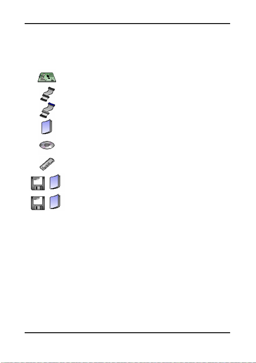
The retail motherboard package should contain the following:
1x Trinity KT400 S2495 motherboard
1x Ultra-DMA-133/100/66/33 IDE cable (One additional for IDE RAID)
1 x Serial ATA Driver Diskette and User’s Manual (Optional)
1x 34-Pin floppy drive ca ble
1x Trinity KT400 S2495 User’s Manual
1x TYAN driver CD
1x I/O shield
If any of these items are missing, please contact your vendor/dealer for replacement before
continuing with the installation process.
1 x IDE RAID Driver Diskette and User’s Manual (Optional)
iii
http://www.tyan.com
Page 4

Trinity KT400 S2495
Chapter 1: Introduction
Chapter 1: Introduction
1.1 – Congratulations!
You have purchased one of the most powerful solutions for the AMD Athlon XP processor, the
Trinity KT400 S2495. Based on VIA’s KT400 chipsets, the main features of the Trinity KT400
S2495 are: ATX form factor, onboard 10/100 Fast Ethernet port, and 6 -channel audio. It also
offers optional features such as Serial ATA and IDE RAID for desktop demands.
Remember to visit TYAN’s Website at http://www.tyan.com . There you can find information on
all of TYAN’s products with FAQs, distributors list, and BIOS setting explanations.
1-1
http://www.tyan.com
Page 5

Trinity KT400 S2495
Chapter 1: Introduction
1.2 – Hardware Specifications
Processors
• Socket A processor
• AMD Athlon™ XP / Athlon™ / Duron™
processor supports up to 3000+ CPU
• Front-Side Bus support for 200/266/333MHz
Chipset
• VIA KT400 North Bridge chipset
• VIA VT8235 South Bridge chipset
• Winbond W83697HF LPC I/O chip
Memory
• Three 184-pin DIMM sockets
• Supports DDR 400*/333/266/200
• Up to 3GB Registered, unbuffered non-ECC
type memory modules
* NOTE: PC2700 maximum to 2 DIMM
support only. PC3200 maximum to 1 DIMM
(DIMM 3) support only. Please go to TYAN
website http://www.TYAN.com for the latest
DDR 400/PC3200 qualified memory test list.
Integrated LAN Controller
• VIA VT6103 PHY 10/100Base-TX Ethernet
controller
• One RJ-45 LAN connector with LEDs
Intelligent Audio
• ALC650 6-Channel AC97 audio CODEC
• Line-in / Speaker-out / MIC-in phone jacks
• CD-in / Aux-in connectors
• SPDIF output connector
Integrated IDE RAID (Optional)
• High Point HPT372N supports IDE RAID 0,
1, 0+1
• Dual IDE channels for ATA 133
Integrated Serial ATA (Optional)
• Silicon Image SiI3112 controller
• Two Serial ATA ports
Integrated PCI IDE
• Dual channel master mode support up to
four IDE devices
• Support for ATA-133 / 100 / 66 IDE drives
and ATAPI compliant devices
Note: TYAN reserves the right to add support or discontinue support for any OS with or
without notice.
Integrated I/O Interface
• One floppy connector supports up to
two drives
• Six USB 2.0 ports (4 ports on rear
panel, 2 ports by pin-header )
• One IrDA connector
Rear Panel I/O ports
• Stacked PS/2 Mouse & Keyboard ports
• Stacked two USB 2.0 ports and RJ45
LAN port on top
• Stacked two USB 2.0 ports
• Two 9-pin UART Serial ports
• One 25-pin SPP/ECP/EPP Parallel port
• Audio jacks
Expansion Slots
• Six 32-bit / 33MHz PCI 2.2 slots
• One 1.5V AGP 4X / 8X slot
BIOS
• Award BIOS 4Mbit Flash ROM
• Support APM 1.2 & ACPI 1.0B
• PnP, DNI 2.0, WFM 2.0 Power
Management
• Jumper free for System over clocking
and over voltage for CPU / Memory /
AGP
Power
• On board VRM, 2-phase PWM
• ATX 20-pin power connector
Regulatory
• EMI - CE, FCC Class B
Miscellaneous
• WOL, STR, Three fan connectors
• POST code 7-segment LED display
Form Factor
• ATX footprint
• 305mm x 245mm (12” x 9.6”)
1-2
http://www.tyan.com
Page 6

Trinity KT400 S2495 Chapter 2: Board Installation
Chapter 2: Board Installation
Installation
You are now ready to install your motherboard. The mounting holes pattern of the Trinity
KT400 S2495 matches the ATX specification. Before continuing with installation, confirm that
your chassis supports a standard ATX motherboard.
How to install our products right…. the first time!
The first thing you should do read this user’s manual. It contains important information that
will make configuration and setup much easier. Here are some precautions you should take
when installing your motherboard:
(1) Ground yourself properly before removing your motherboard from the antistatic bag.
Unplug the power from your computer power supply and then touch a safely
grounded object to release static charge (i.e. power supply case). For the safest
conditions, TYAN recommends wearing a static safety wrist strap.
(2) Hold the motherboard by its edges and do not touch the bottom of the board, or flex
the board in any way.
(3) Avoid touching the motherboard components, IC chips, connectors, memory
modules and leads.
(4) Place the motherboard on a grounded antistatic surface or on the antistatic bag that
the board was shipped in.
(5) Inspect the board for damage.
The following pages include details on how to install your motherboard into your chassis, as
well as installing the processor, memory, disk drives and cables.
Note: DO NOT APPLY POWER TO THE BOARD IF IT HAS BEEN DAMAGED
2-1
http://www.tyan.com
Page 7
Trinity KT400 S2495 Chapter 2: Board Installation
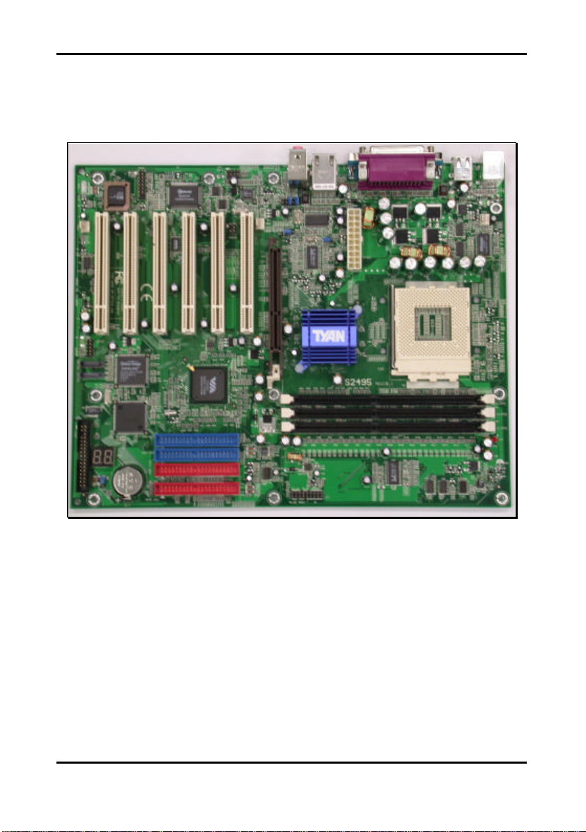
2.1 – Board Image
The following is an image of the Trinity KT400 S2495.
The above photograph is purely representative. Due to engineering updates and new
board revisions, certain components may change and or be repositioned. The picture
above may or may not look exactly like the board you received.
The following page includes details on the vital components of this motherboard.
2-2
http://www.tyan.com
Page 8
Trinity KT400 S2495 Chapter 2: Board Installation
S2495
111
1
KB1
USB1
COM1
COM2
LPT1
FAN1
ATX1
USB2
AUD2
AUD1
VT6103
VIA KT400
1217
18
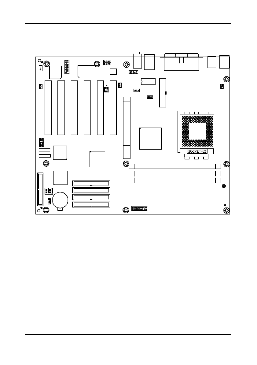
2.2 – Board Parts
Ÿ
1
1
ALC650
SPDIF1
CD1
AUX1
FAN3
1
JCK1
AGP1
JCK2
WOL
1
FAN2
BIOS
1
GAME1
W83697HF
CPU
LED1
(Optional)
(Optional)
1
FDD
SATA2
SATA1
USB3
LED2
1
CMOS
SII3112
(Optional)
HPT372N
(Optional)
BAT1
VT8235
PRI-IDE
SEC-IDE
RAID IDE2
RAID IDE1
PCI1PCI2PCI3PCI4PCI5PCI6
VIA
(Optional)
(Optional)
VT8377
DIMM1
DIMM2
DIMM3
J1
This jumper diagram is representative of the latest board revision available at the time
of publishing. The board you receive may or may not look exactly like the above
diagram. The board parts are not to scale.
2-3
http://www.tyan.com
Page 9
Trinity KT400 S2495 Chapter 2: Board Installation
S2495
111
1
KB1
USB1
COM1
COM2
LPT1
FAN1
ATX1
USB2
AUD2
AUD1
VT6103
VIA KT400
CMOS
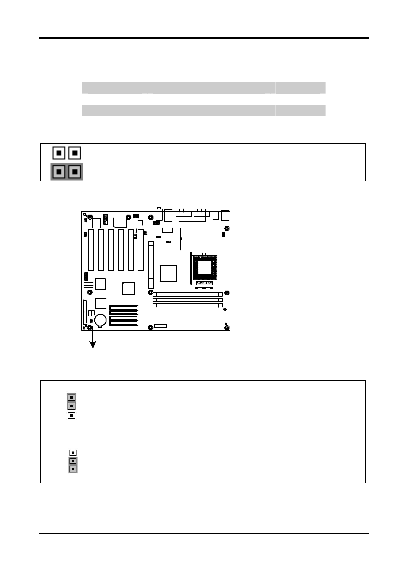
2.3 – Jumper Settings & Definitions
Jumper Example
CMOS Reset (CMOS)
Jumper Function Ref. Page
CMOS Clear CMOS Page 2-4
JCK1 FSB Select Page 2-5
JCK2 FSB Select Page 2-5
Jumper OFF – open (without jumper cap)
Jumper ON – closed (with jumper cap)
W83697HF
1
CD1
AUX1
1
ALC650
SPDIF1
1
FAN3
JCK1
AGP1
JCK2
1
BIOSWOL
GAME1
1
FAN2
(Optional)
(Optional)
1
Normal
1
Clear CMOS
CPU
DIMM1
DIMM2
DIMM3
LED1
PRI-IDE
SEC-IDE
RAID IDE2
RAID IDE1
PCI1PCI2PCI3PCI4PCI5PCI6
VT8377
VIA
VT8235
(Optional)
(Optional)
J1
1
USB3
SII3112
SATA2
(Optional)
SATA1
FDD
HPT372N
(Optional)
LED2
1
BAT1
CMOS
You can reset the CMOS settings in case an incorrect setting causes
system instability or you have forgotten your system/setup password or
have just flashed your BIOS by using these jumpers.
- Power off system, disconnect power supply from motherboard
- Set jumper to Clear CMOS
- Wait about 5 seconds
- Set jumper to Normal (Default)
2-4
http://www.tyan.com
Page 10
Trinity KT400 S2495 Chapter 2: Board Installation
S2495
1
KB1
USB1
COM1
COM2
LPT1
FAN1
ATX1
VIA KT400
JCK1
JCK1
JCK2
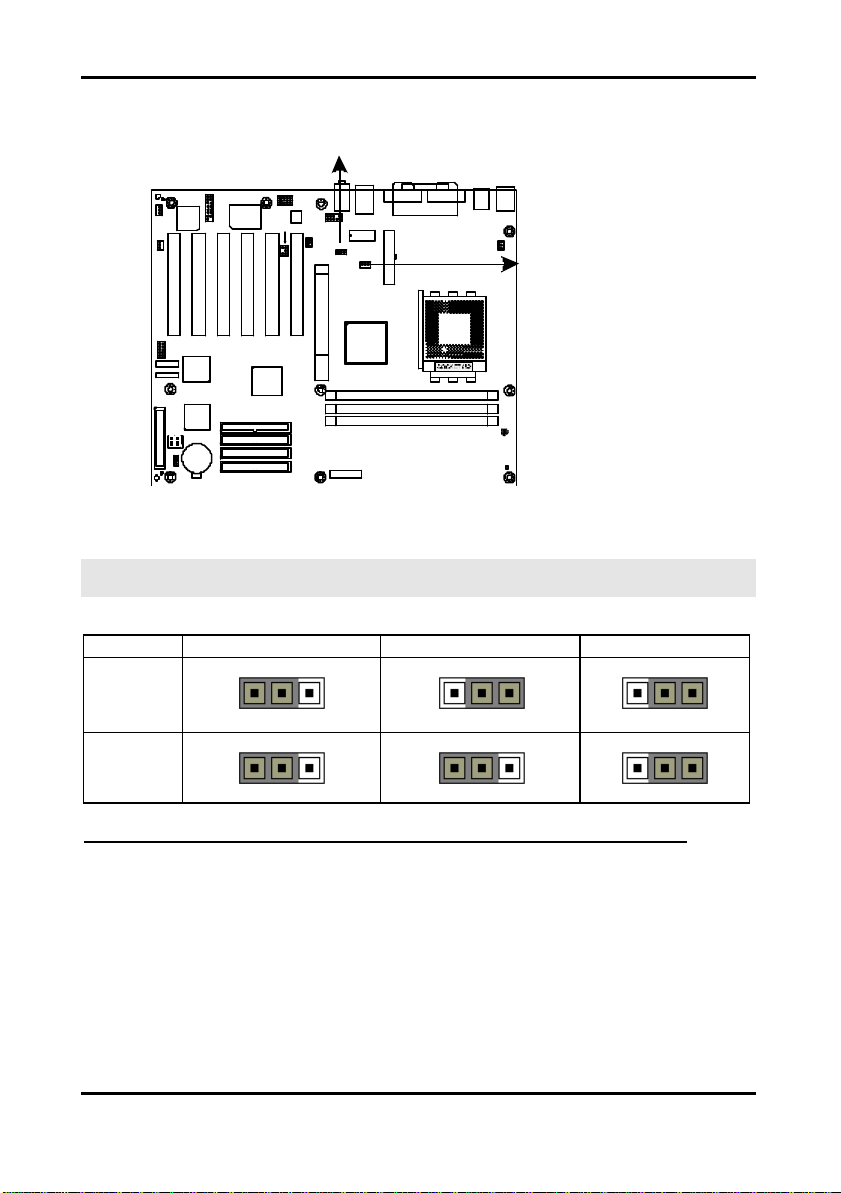
CPU FSB Select (JCK1 & JCK2)
W83697HF
PRI-IDE
SEC-IDE
RAID IDE2
RAID IDE1
VT8235
1
CD1
AUX1
1
ALC650
SPDIF1
1
PCI1PCI2PCI3PCI4PCI5PCI6
VIA
(Optional)
(Optional)
USB2AUD2
1
AUD1
VT6103
FAN3
JCK1
1
1
AGP1
JCK2
DIMM1
DIMM2
DIMM3
CPU
LED1
VT8377
J1
1
BIOSWOL
GAME1
1
FAN2
1
USB3
(Optional)
SII3112
SATA2
(Optional)
(Optional)
SATA1
FDD
HPT372N
(Optional)
LED2
1
BAT1
CMOS
Note:
Ÿ For software FSB programming by BIOS SETUP utility, JCK1 and JCK2 have to
place at Default (see 3.9 – Frequency/Voltage Control).
JCK# 100MHz*(Default) 133MHz 166MHz
1 3
1 3
. 1 3
JCK1
1 3
1 3
1 3
JCK2
About the jumpers setting (JCK1 & JCK2) please see the following information:
1. If JCK1 and JCK2 are left in their default settings (100MHz) then the BIOS will
automatically detect a 100MHz or 133MHz CPU automatically.
2. If you want to use a 333MHz CPU then you will need to manually change the jumpers to
the 166MHz setting, however if you set the CPU FSB to this speed then you'll only be
able to run the memory at DDR333.
2-5
http://www.tyan.com
Page 11
Trinity KT400 S2495 Chapter 2: Board Installation
18
17
(12, 14, 16, 18) SPEAKER
BUTTON
2.4 – Connector Description
* SATA and IDE RAID are optional functions.
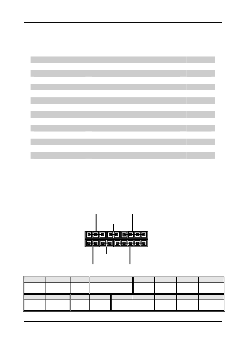
Front Panel Connector (J1)
Your chassis will usually come with connectors to install onto the motherboard, such as HD
and Power LEDs. The Front Panel Connector (J1) has been implemented for such purposes.
Connector Function Ref. Page
J1 Front panel connector Page 2-6
LED1 Power On LED Page 2-7
LED2 Post error code for BIOS Page 5-7
FAN1 CPU fan connector Page 2-7
FAN2 Chassis fan connector Page 2-7
FAN3 Power fan connector Page 2-7
USB3 USB header #3 Page 2-8
WOL Wake On LAN Page 2-8
CD1 CD Audio-in connector Page 2-9
AUX1 Auxiliary Line-In connector Page 2-9
AUD1 Front Audio Page 2-10
GAME1 Game port connector Page 2-10
SPDIF1 Sony/Philips Digital InterFace connector Page 2-11
SATA1/SATA2* Serial ATA connector Page 2-11
RAID IDE1/RAID IDE2*
IDE RAID connector Page 2-12
(2, 4, 6) PW-LED
(8, 10) PW-ON
Pin 2
POWER
_ LED
Pin 1
VCC HDD_LED GND REST
2
1
(5, 7) RESET
(1, 3) HD-LED
Pin 4 Pin 6 Pin 8 Pin 10 Pin 12 Pin 14 Pin 16 Pin 18
GND GND POWER
BUTTON
Pin 3 Pin 5 Pin 7 Pin 9 Pin 11 Pin 13 Pin 15 Pin 17
(9, 11, 13, 15, 17) IR
GND
VCC CIRRX IRRX
2-6
http://www.tyan.com
VCC GND NC SPEAKER
GND IRTX
Page 12
Trinity KT400 S2495 Chapter 2: Board Installation
S2495
1
111
KB1
USB1
FAN1
VIA KT400
LED1
S2495
1
111
KB1
USB1
COM1
FAN1
VIA KT400
FAN1
FAN3
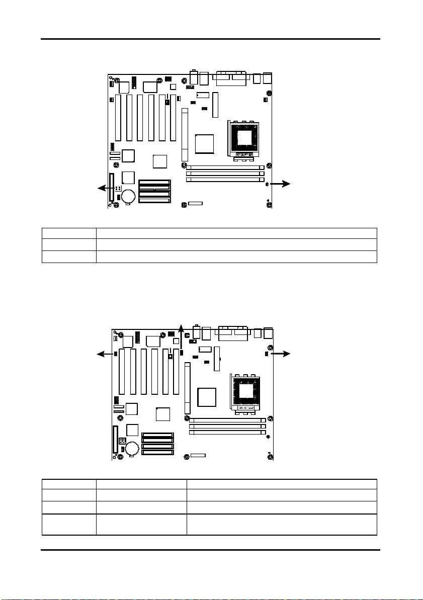
LED Information (LED1 & LED2)
W83697HF
ALC650
SPDIF1
1
CD1
USB2AUD2
AUX1
1
AUD1
1
VT6103
FAN3
JCK1
AGP1
JCK2
COM1COM2
LPT1
ATX1
1
BIOS
WOL
GAME1
1
FAN2
CPU
DIMM1
DIMM2
DIMM3
LED1
LED2
(Optional)
(Optional)
PCI3
PRI-IDE
SEC-IDE
RAID IDE2
RAID IDE1
VT8235
PCI1PCI2
VT8377
VIA
(Optional)
(Optional)
J1
PCI4
PCI5PCI6
1
USB3
SII3112
SATA2
(Optional)
SATA1
FDD
HPT372N
(Optional)
LED2
1
BAT1
CMOS
LEDs Description
LED1 Power on LED
LED2 Post error code for BIOS (Ref. Appendix II)
Fan Connector (FAN1 & FAN2 & FAN3)
W83697HF
PRI-IDE
SEC-IDE
RAID IDE2
RAID IDE1
VT8235
1
CD1
AUX1
1
ALC650
SPDIF1
1
FAN3
AGP1
PCI1PCI2PCI3PCI4PCI5PCI6
VIA
(Optional)
(Optional)
COM2
USB2AUD2
VT6103
VT8377
LPT1
ATX1
JCK2
CPU
DIMM1
DIMM2
DIMM3
J1
LED1
AUD1
JCK1
FAN2
(Optional)
(Optional)
1
BIOS
WOL
GAME1
1
FAN2
1
USB3
SII3112
SATA2
(Optional)
SATA1
FDD
HPT372N
(Optional)
LED2
1
BAT1
CMOS
Fan # Description Functions
1 CPU fan RPM Read and controlled
2 Chassis fan RPM Read and controlled
3 P ower fan The fan connector does not support RPM function
which can not detect speed of the fan.
2-7
http://www.tyan.com
Page 13
Trinity KT400 S2495 Chapter 2: Board Installation
S2495
111
11111
KB1
USB1
COM1
COM2
LPT1
FAN1
ATX1
USB2
AUD2
AUD1
VT6103
VIA KT400
156
10
S2495
111
11111
KB1
USB1
COM1
COM2
LPT1
FAN1
ATX1
USB2
AUD2
AUD1
VT6103
VIA KT400
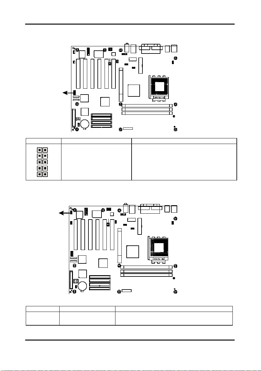
USB3 Connector
1
BIOSWOL
GAME1
FAN2
W83697HF
ALC650
SPDIF1
CD1
AUX1
FAN3
JCK1
AGP1
JCK2
DIMM1
DIMM2
DIMM3
CPU
LED1
USB3
(Optional)
(Optional)
PRI-IDE
SEC-IDE
RAID IDE2
RAID IDE1
PCI1PCI2PCI3PCI4PCI5PCI6
VIA
VT8235
(Optional)
(Optional)
VT8377
J1
1
USB3
SII3112
SATA2
(Optional)
SATA1
FDD
HPT372N
(Optional)
LED2
1
BAT1
CMOS
Connector Description Functions
Pin 1: VCC
Pin 2: - Data
Pin 3: +Data
Pin 4: GND
Pin 5: GND
Pin 6: GND
Pin 7: GND
Pin 8: +Data
Pin 9: - Data
Pin 10: VCC
Use the USB3 header here for front panel
USB 2.0 connectors (via an optional cable)
WOL Connector
WOL
(Optional)
(Optional)
1
BIOS
WOL
GAME1
FAN2
1
USB3
SII3112
SATA2
(Optional)
SATA1
FDD
HPT372N
(Optional)
LED2
1
BAT1
CMOS
W83697HF
PRI-IDE
SEC-IDE
RAID IDE2
RAID IDE1
VT8235
CD1
AUX1
ALC650
SPDIF1
FAN3
JCK1
AGP1
JCK2
DIMM2
DIMM3
CPU
DIMM1
LED1
PCI1PCI2PCI3PCI4PCI5PCI6
VIA
(Optional)
(Optional)
VT8377
J1
Connector
Description Functions
WOL Wake On LAN Reserved for a network interface card to wake the
system from power saving mode.
2-8
http://www.tyan.com
Page 14
Trinity KT400 S2495 Chapter 2: Board Installation
S2495
111
1
KB1
USB1
COM1
COM2
LPT1
FAN1
ATX1
USB2
AUD2
AUX1
AUD1
ALC650
SPDIF1
VT6103
VIA KT400
(Optional)
(Optional)
CD1
S2495
111
1
KB1
USB1
COM1
COM2
LPT1
FAN1
ATX1
USB2
AUD2
AUX1
AUD1
ALC650
SPDIF1
VT6103
VIA KT400
(Optional)
(Optional)
AUX1
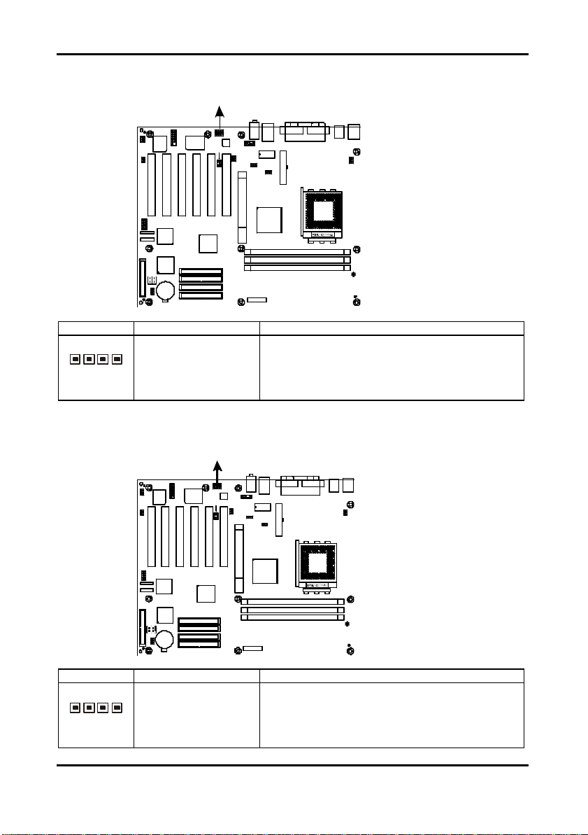
CD1 Connector (CD Audio -In)
W83697HF
PRI-IDE
SEC-IDE
RAID IDE2
RAID IDE1
1
CD1
1
FAN3
1
AGP1
PCI1PCI2PCI3PCI4PCI5PCI6
VIA
VT8235
(Optional)
(Optional)
1
BIOS
WOL
GAME1
1
FAN2
1
USB3
SII3112
SATA2
(Optional)
SATA1
FDD
HPT372N
(Optional)
LED2
1
BAT1
CMOS
Connector
Description Functions
Pin 1: CD_In_Left
Pin 2: CD_Reference
1 4
Pin 3: CD_Reference
Pin 4: CD_In_Right
AUX1 Connector (Auxiliary Line-In)
W83697HF
1
CD1
1
FAN3
1
AGP1
1
BIOS
WOL
GAME1
1
FAN2
JCK1
JCK2
VT8377
J1
CPU
DIMM1
DIMM2
DIMM3
LED1
Connect CD-ROM (DVD) audio out
JCK1
JCK2
Connector
1 4
CPU
DIMM1
DIMM2
DIMM3
(Optional)
(Optional)
PCI3
PRI-IDE
SEC-IDE
RAID IDE2
RAID IDE1
VT8235
PCI1PCI2
VT8377
VIA
J1
PCI4
1
PCI5PCI6
USB3
SII3112
SATA2
(Optional)
SATA1
FDD
HPT372N
(Optional)
LED2
1
BAT1
CMOS
Description Functions
Pin 1: Lift Line_In
Connect other devices audio out
Pin 2: GND
Pin 3: GND
Pin 4: Right Line_In
2-9
http://www.tyan.com
LED1
Page 15
Trinity KT400 S2495 Chapter 2: Board Installation
S2495
111
1
KB1
USB1
COM1
COM2
LPT1
FAN1
ATX1
USB2
AUD2
AUX1
AUD1
ALC650
SPDIF1
VT6103
VIA KT400
(Optional)
(Optional)
AUD1
2110
2110
S2495
111
1
KB1
USB1
COM1
COM2
LPT1
FAN1
ATX1
USB2
AUD2
AUX1
AUD1
ALC650
SPDIF1
VT6103
VIA KT400
(Optional)
(Optional)
GAME1
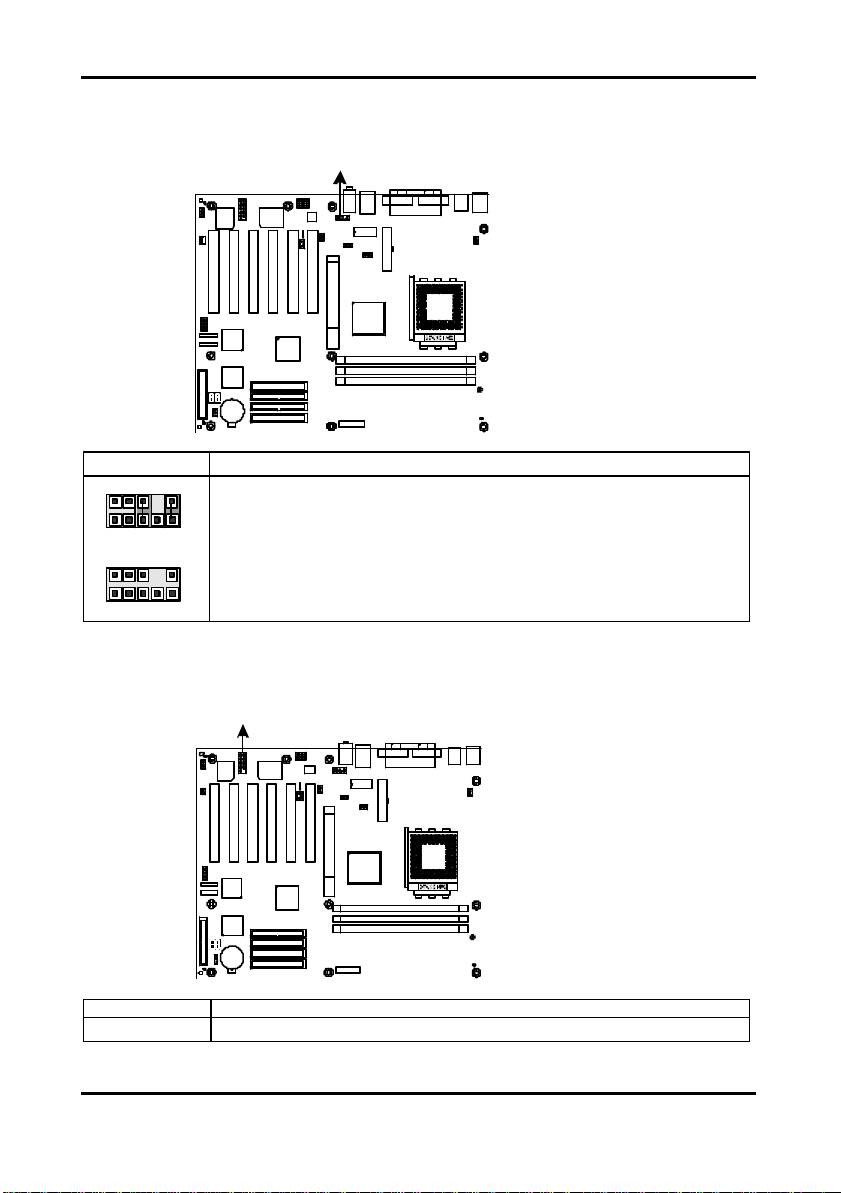
AUD1 Connector
WOL
1
FAN2
1
USB3
(Optional)
SATA2
(Optional)
SATA1
FDD
LED2
1
CMOS
AUD1
.
9
9
GAME1 Connector
WOL
1
FAN2
W83697HF
PRI-IDE
SEC-IDE
RAID IDE2
RAID IDE1
1
CD1
1
1
FAN3
JCK1
AGP1
JCK2
PCI1PCI2PCI3PCI4PCI5PCI6
VT8377
VIA
VT8235
J1
CPU
DIMM1
DIMM2
DIMM3
LED1
1
BIOS
GAME1
SII3112
(Optional)
HPT372N
(Optional)
BAT1
Description
Jumper 5-6, 9-10 = Rear panel audio output (Default)
Jumper open = Front panel audio output (via an optional cable)
1
1
BIOS
GAME1
W83697HF
CD1
1
1
FAN3
JCK1
AGP1
JCK2
Connector Description
CPU
DIMM1
DIMM2
DIMM3
LED1
(Optional)
(Optional)
PRI-IDE
SEC-IDE
RAID IDE2
RAID IDE1
PCI1PCI2PCI3PCI4PCI5PCI6
VT8377
VIA
VT8235
J1
1
USB3
SII3112
SATA2
(Optional)
SATA1
FDD
HPT372N
(Optional)
LED2
1
BAT1
CMOS
GAME1 Game port connector (via an optional cable)
2-10
http://www.tyan.com
Page 16
Trinity KT400 S2495 Chapter 2: Board Installation
S2495
1111111
1
KB1
USB1
COM1
COM2
LPT1
FAN1
ATX1
USB2
AUD2
AUD1
VT6103
VIA KT400
2
6
S2495
1111111
1
KB1
USB1
COM1
COM2
LPT1
FAN1
ATX1
USB2
AUD2
AUD1
VT6103
VIA KT400
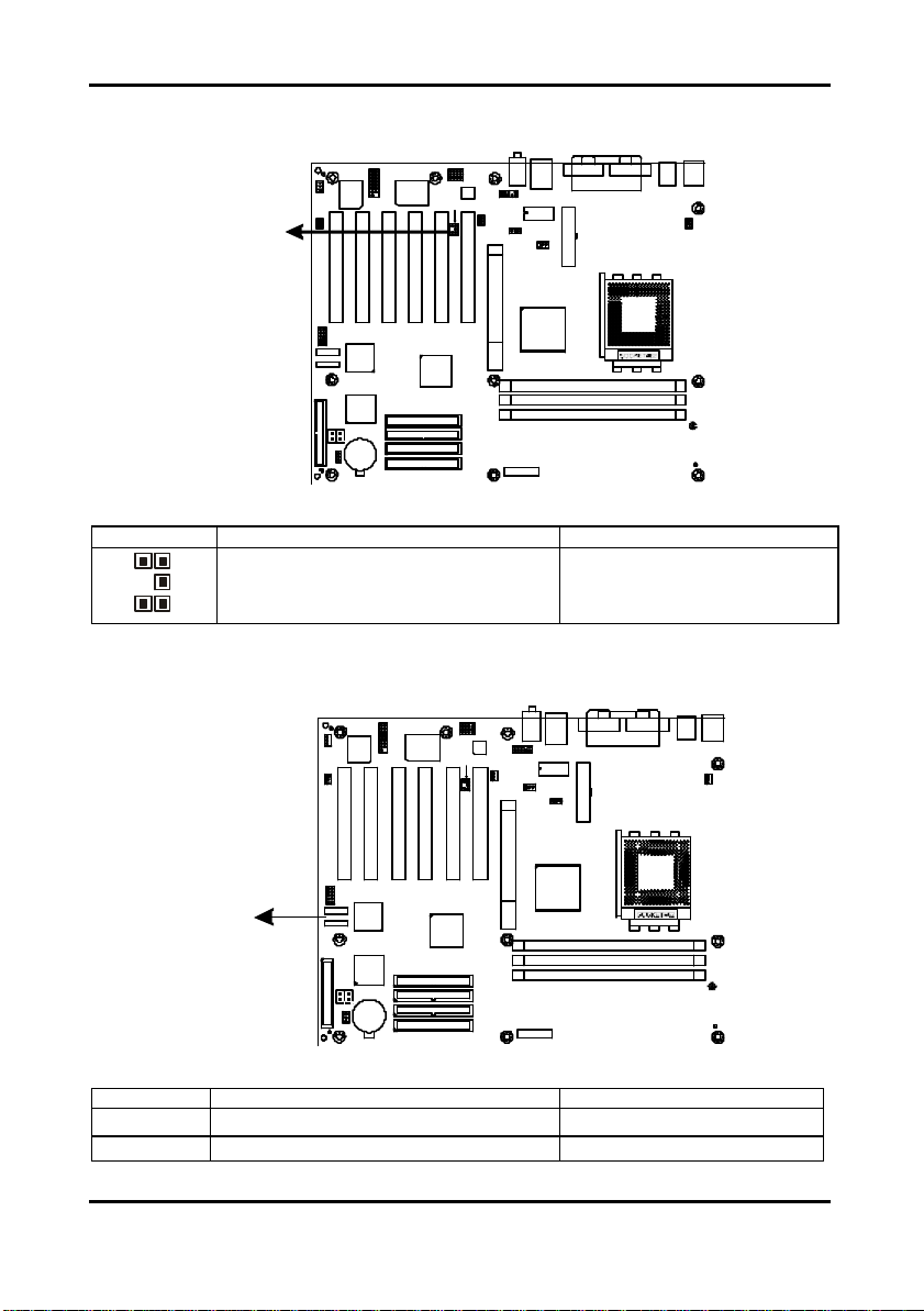
SPDIF1 Connector
SPDIF1
1
W83697HF
BIOS
WOL
GAME1
FAN2
ALC650
SPDIF1
CD1
AUX1
FAN3
JCK1
AGP1
JCK2
PCI3
PRI-IDE
SEC-IDE
RAID IDE2
RAID IDE1
VT8235
PCI1PCI2
VIA
(Optional)
(Optional)
VT8377
J1
(Optional)
(Optional)
PCI4
PCI5PCI6
1
USB3
SII3112
SATA2
(Optional)
SATA1
FDD
HPT372N
(Optional)
LED2
1
BAT1
CMOS
CPU
DIMM1
DIMM2
DIMM3
LED1
Connector Description Functions
1
Pin 1: VCC
Pin 3: Non
5
Pin 5: SPDIF_IN
Pin 2: SPDIF_OUT
Pin 4: NC
Pin 6: GND
Sony/Philips Digital InterFace
connector (via an optional cable)
SATA1 / SATA2 Connectors (Optional)
SATA2
SATA1
(Optional)
(Optional)
1
W83697HF
BIOS
WOL
GAME1
FAN2
1
USB3
SII3112
SATA2
(Optional)
SATA1
FDD
HPT372N
(Optional)
LED2
1
BAT1
CMOS
PRI-IDE
SEC-IDE
RAID IDE2
RAID IDE1
VT8235
CD1
AUX1
ALC650
SPDIF1
FAN3
JCK1
AGP1
JCK2
DIMM1
DIMM2
DIMM3
CPU
LED1
PCI1PCI2PCI3PCI4PCI5PCI6
VIA
(Optional)
(Optional)
VT8377
J1
Connector
Description Functions
SATA1 Serial ATA connector Supports serial ATA devices
SATA2 Serial ATA connector Supports serial ATA devices
2-11
http://www.tyan.com
Page 17
Trinity KT400 S2495 Chapter 2: Board Installation
S2495
111
1
KB1
USB1
COM1
COM2
LPT1
FAN1
ATX1
USB2
AUD2
AUD1
VT6103
VIA KT400
RAID IDE1
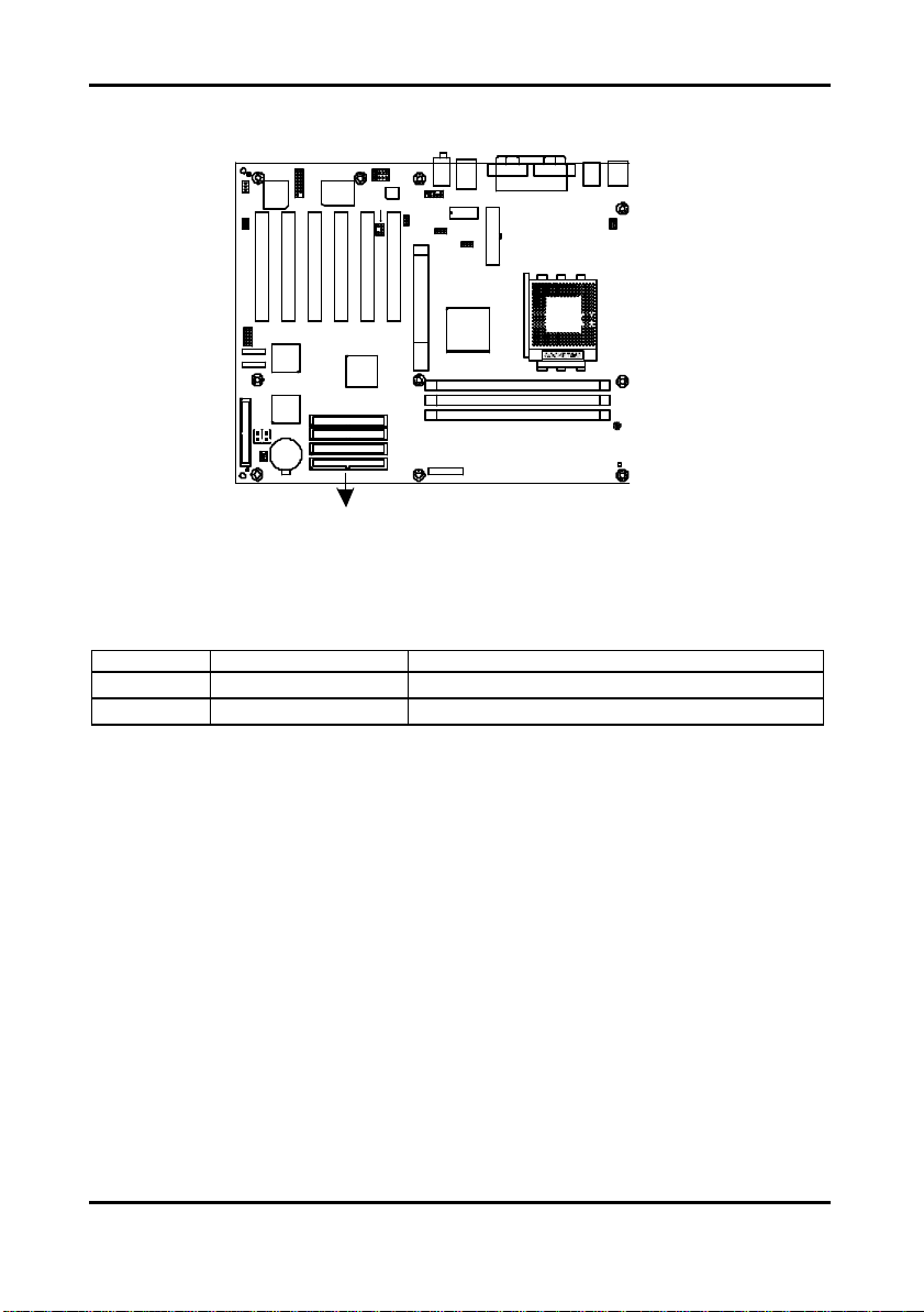
RAID IDE1 / RAID IDE2 Connectors (Optional)
W83697HF
ALC650
SPDIF1
1
CD1
AUX1
1
FAN3
1
JCK1
AGP1
JCK2
1
BIOS
WOL
GAME1
1
FAN2
DIMM1
DIMM2
DIMM3
CPU
LED1
(Optional)
(Optional)
PCI3
PRI-IDE
SEC-IDE
RAID IDE2
RAID IDE1
VT8235
PCI1PCI2
VIA
(Optional)
(Optional)
VT8377
J1
PCI4
PCI5PCI6
1
USB3
SII3112
SATA2
(Optional)
SATA1
FDD
HPT372N
(Optional)
LED2
1
BAT1
CMOS
RAID IDE2
Connector
Description Functions
RAID IDE1 IDE RAID connector Supports IDE RAID 0, 1, 0+1
RAID IDE2 IDE RAID connector Supports IDE RAID 0, 1, 0+1
2-12
http://www.tyan.com
Page 18
Trinity KT400 S2495 Chapter 2: Board Installation
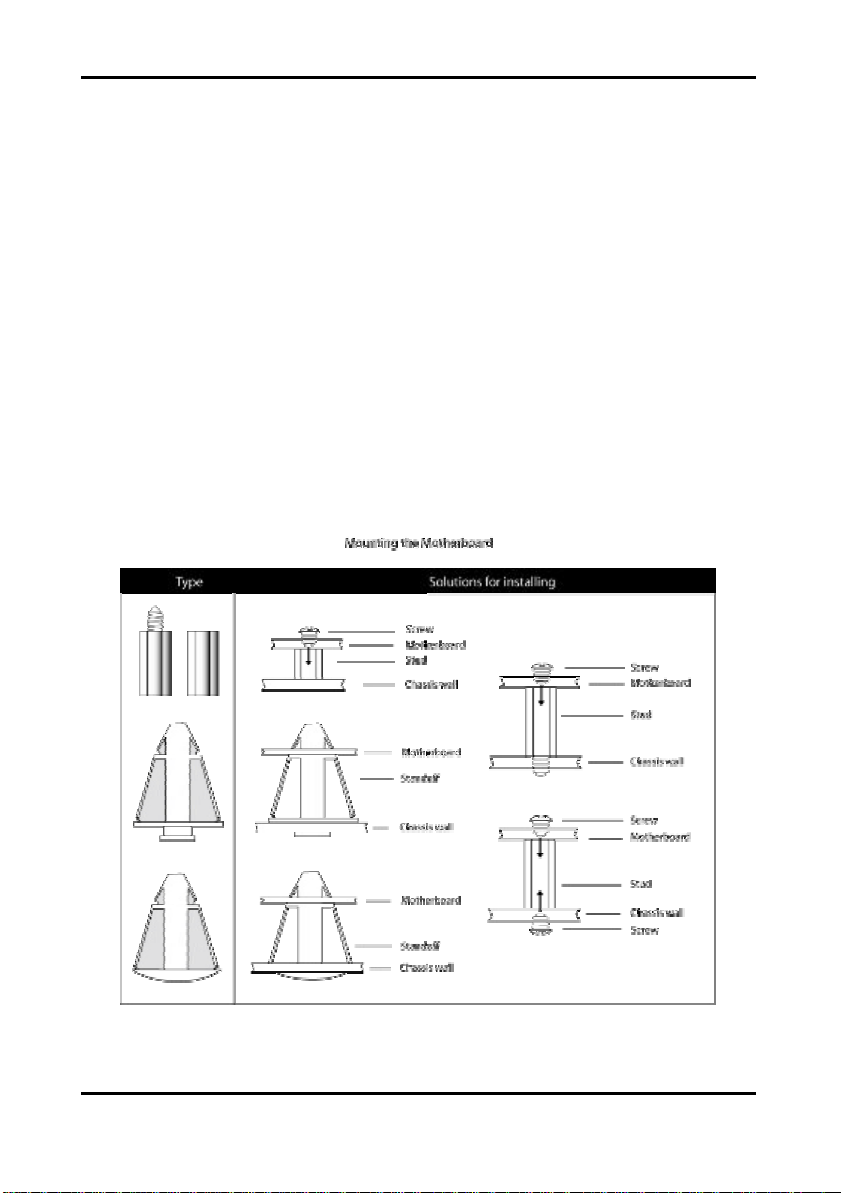
2.5 – Mounting the Motherboard
Before installing your motherboard, make sure your chassis has the necessary motherboard
support studs installed. These studs are usually metal and are gold in color. Usually, the
chassis manufacturer will pre-install the support studs. If you’re unsure of stud placement,
simply lay the motherboard inside the chassis and align the screw holes of the motherboard to
the studs inside the case. If there are any studs missing, you will know right away since the
motherboard will not be able to be securely installed.
Some chassis’ include plastic studs instead of metal. Although the plastic studs are usable,
TYAN recommends using metal studs with screws that will fasten the motherboard more
securely in place.
- Memory Type: The S2495 Trinity KT400 supports Registered, unbuffered non-ECC type
memory modules.
- CPU Front-Side Bus Speed Match: When the CPU FSB is 333MHz, you must to use
DDR333 (PC2700) memory modules.
Below is a chart detailing what the most common motherboard studs look like and how they
should be installed it.
TIP: Use metal studs if possible, as they hold the motherboard into place more securely than
plastic standoffs.
2-13
http://www.tyan.com
Page 19
Trinity KT400 S2495 Chapter 2: Board Installation
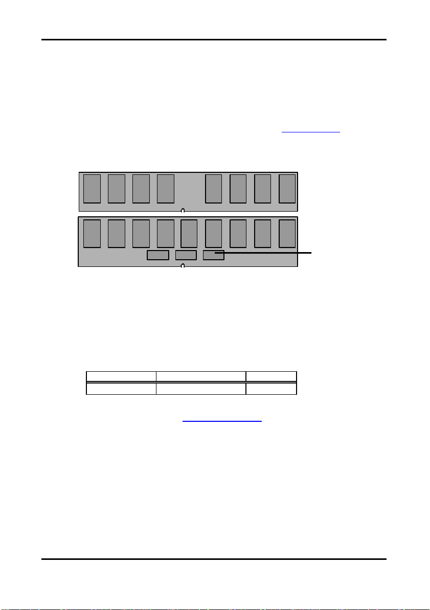
Registered DDR SDRAM
chips near the
2.6 – Installing the Memory
Before attempting to install any memory, make sure that the memory you have is compatible
with the motherboard as well as the processor. For example, while PC1600 DDR modules are
compatible with all DDR based motherboards, they will not work if you are required to run the
motherboard and processor buses at 133MHz. For this, PC2100 DDR modules are required.
Critically important is whether you’re using the recommended memory for the current board
you have. For this information, please check T YAN’s web site at: www.tyan.com
The following diagram shows the types of RAM modules you may encounter depending on
your board:
DDR Unbuffered
Registered
memory has
extra buffer
bottom
Here are a few key points to note before installing memory into your Trinity KT400 S2495:
• 128MB, 256MB, 512MB and 1GB Registered, unbuffered non -ECC
PC1600/PC2100/PC2700/PC3200* DDR memory modules are supported
• All installed memory will be automatically detected - no need to set any jumpers
• The Trinity KT400 S2495 supports up to 3GB of memory
* NOTE: DDR400/PC3200 Qualified Memory Test List:
Vendor Type Size
ADATA winbond
PC2700 maximum to 2 DIMM support only. PC3200 maximum to 1 DIMM (DIMM 3)
support only.
Please go to TYAN website http://www.TYAN.com for the latest DDR400/PC3200
qualified memory test list.
W942508BH -5 256MB
2-14
http://www.tyan.com
Page 20
Trinity KT400 S2495 Chapter 2: Board Installation
2.7 – Memory Installation Procedure
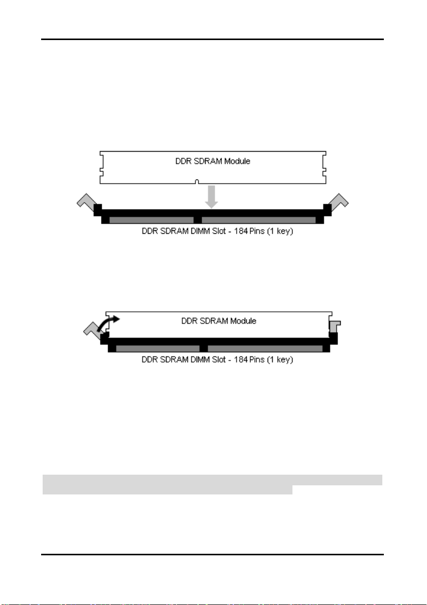
When installing memory modules, make sure the modules align properly with the memory
socket. There should be keys (small indents) on your memory modules that fit according to the
keys in the memory socket. DDR modules and sockets have only one key, which is slightly
near the center of the module/socket. SDRAM modules (also referred to as PC100 or PC133)
and their sockets have two keys and will not insert into DDR DIMM sockets. The method of
installing memory modules is detailed in the following diagrams.
Once the memory modules are firmly seated in the socket, two clamps on either side will close
and secure the module into the socket. Sometimes you may need to close the clamps
manually.
To remove the memory module, simply push the clamps outwards until the memory module
pops up. Then simply remove the module.
TIP: When installing memory, a module may require a considerable amount of force to seat
properly, although this is very rare. To avoid bending and damaging your motherboard, place
it on its anti-static bag and onto a flat surface, and then proceed with memory installation.
Note: YOU MUST unplug the power connector to the motherboard before performing system
hardware changes, to avoid damaging the board or expansion device
2-15
http://www.tyan.com
Page 21
Trinity KT400 S2495 Chapter 2: Board Installation
2.8 – Installing the Processor and Heats ink
Your Trinity KT400 S2495 supports the latest processor technologies from AMD. Check the
following page on TYAN’s website for latest process or support:
http://www.tyan.com
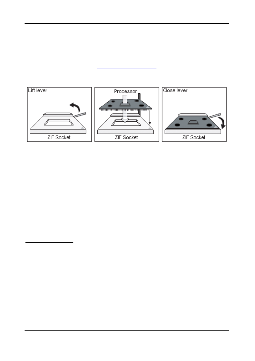
The following diagrams will detail how to install your processor(s):
The diagram is provided as a visual guide to help you install socket processors and may not
be an exact representation of the processors you have.
1. Lift the lever on the socket until it is approximately 90o or as far back as
possible to the socket.
2. Align the processor with the socket. There are keyed pins underneath the processor
to ensure that the processor’s installed correctly.
3. Seat the processor firmly into the socket by gently pressing down until the processor
sits flush with the socket.
4. Place the socket lever back down until it locks into place.
5. Your processor is installed.
Take care when installing processors as they have very fragile connector pins below
the processor and can bend and break if inserted improperly.
Heatsink Installation
After you are done installing the processor(s), you should proceed to installing the heatsinks.
Heatsinks will ensure that the processors do not overheat and continue to operate at
maximum performance for as long as you own them. Overheated processors are also
dangerous to the health of the motherboard.
Because there are many different types of heatsinks available from many different
manufacturers, a lot of them have their own method of installation. For the safest method of
installation and information on choosing the appropriate heatsink, please refer to AMD’s
website at www.amd.com.
2-16
http://www.tyan.com
Page 22
Trinity KT400 S2495 Chapter 2: Board Installation
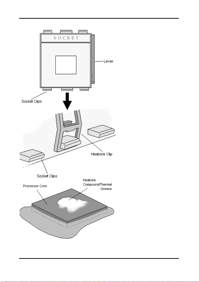
The following diagram will illust rate how to install the most common heatsinks:
First, use thermal compound
(also called heatsink compound
or thermal grease) and apply a
small amount on to the
processor’s core (applying too
much will actually reduce the
cooling) – the small shiny
square in the center of the
processor.
You may then use a small soft
plastic tool, like a credit card to
gently smear a thin layer of
heatsink compound as evenly
as you can across the core.
Because one side of the socket
is raised (and usually has
“SOCKET” imprinted into it)
heatsinks have an indent on one
side to secure flush with the
raised side of the socket.
Then clip one side of the
heatsink onto the socket and
then lay the heatsink flat onto
the processor. Then clip the
other end of the heatsink down
either with your finger or by
using a flathead screwdriver.
Be sure to carefully observe
which side your heatsink is
seated before securing it down
to avoid damaging the
processor, the heatsink or both.
This is will probably be the most
difficult portion of setting up your
computer so please exercise
caution. TYAN will not accept
responsibility and no warranty
will be given for damage due to
improperly installed heatsinsks.
2-17
http://www.tyan.com
Page 23
Trinity KT400 S2495 Chapter 2: Board Installation
Finishing Installing the Heatsink
After you finish installing the heatsink onto the processor and socket, attach the end wire of
the fan (which should already be attached to the heatsink) to the motherboard. The following
diagram illustrates how to connect fans onto the motherboard.
After you’re finished installing all the fans you can connect your drives (hard drives, CD-ROM
drives, etc.) to your motherboard.
2.9 – Attaching Drive Cables
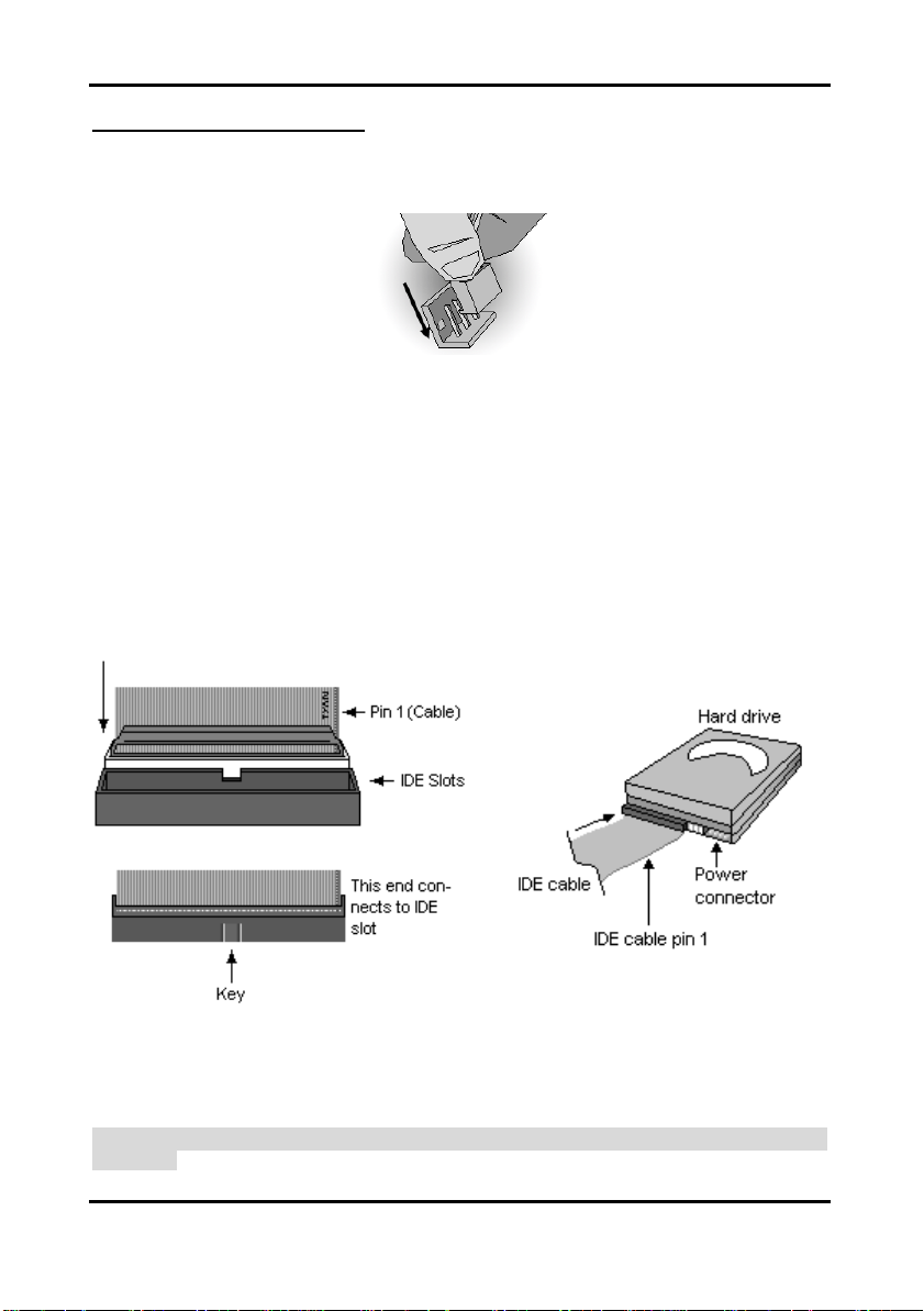
Attaching IDE drive cabling is simple. These cables are “keyed” to only allow them to be
connected in the correct manner. TYAN motherboards have two on-board IDE channels, each
supporting two drives. The PRI-IDE connector designates the Primary channel, while the
SEC-IDE connector designates the Secondary channel.
Attaching IDE cables to the IDE connectors is illustrated below:
Simply plug in the BLUE END of the IDE cable into the motherboard IDE connector, and the
other end(s) into the drive(s). Each standard IDE cable has three connectors, two of which are
closer together. The BLUE connector that is furthest away from the other two is the end that
connects to the motherboard. The other two connectors are used to connect to drives.
TIP: Pin 1 on the IDE cable (usually designated by a colored wire) faces the drive’s power
connector.
http://www.tyan.com
2-18
Page 24
Trinity KT400 S2495 Chapter 2: Board Installation
Floppy Drives
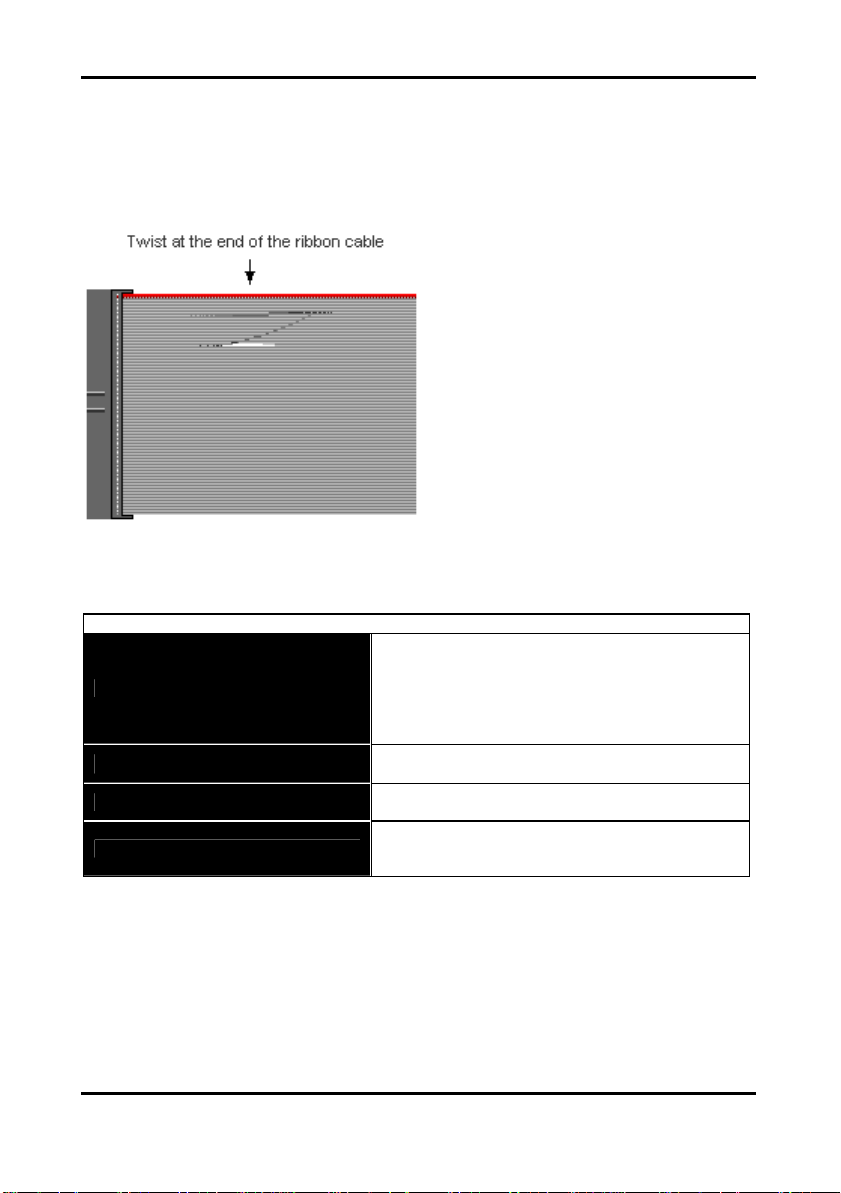
Attaching a floppy drive can be done in a similar manner to an IDE drive. See the diagram
below for an example of a floppy cable. Most of the current floppy drives on the market require
that the cable be installed with the colored stripe positioned next to the power connector. In
most cases, there will be a key pin on the cable which will force proper connection of the cable.
Below are some symptoms of incorrectly installed floppy drives. While they are minor and
installing them incorrectly doesn’t cause severe problems, it may cause your system to freeze
or crash when trying to read and/or write to diskettes.
Symptoms of incorrectly installed floppy drives
Drive is not automatically detected
Drive Fail message at bootup
Drive does not power on
Drive activity light is constantly on
The first floppy drive (commonly denoted as A:)
is usually attached to the end of the cable with
the twist in it. Drive B: is usually connected to
the second or third connector in the cable (the
second or third connector after you install Drive
A:).
Refer to your floppy drive’s installation
instructions (if available), or contact your dealer
if you are unsure about how to attach the
floppy drive(s). Remember, you can only have
2 floppy drives connected at any given time.
Usually caused by faulty cables, cables put in
backwards or a bad floppy drive or motherboard.
Try another floppy drive to verify the problem if
the cable is properly installed or try replacing the
actual cable. Also check to see if the onboard
floppy controller is enabled in the BIOS setup.
The cable, floppy drive or motherboard may be
faulty. Try another drive or cable to verify.
Check power cable and cabling. Maybe a bad
power supply or drive cable problem.
Usually signifies that the cable on the drive is on
backwards, which is a common issue. Reverse
the cable at the floppy drive end and try again.
2-19
http://www.tyan.com
Page 25
Trinity KT400 S2495 Chapter 2: Board Installation
AGP Slot - 1.5 Volts
2.10 – Installing Add-In Cards
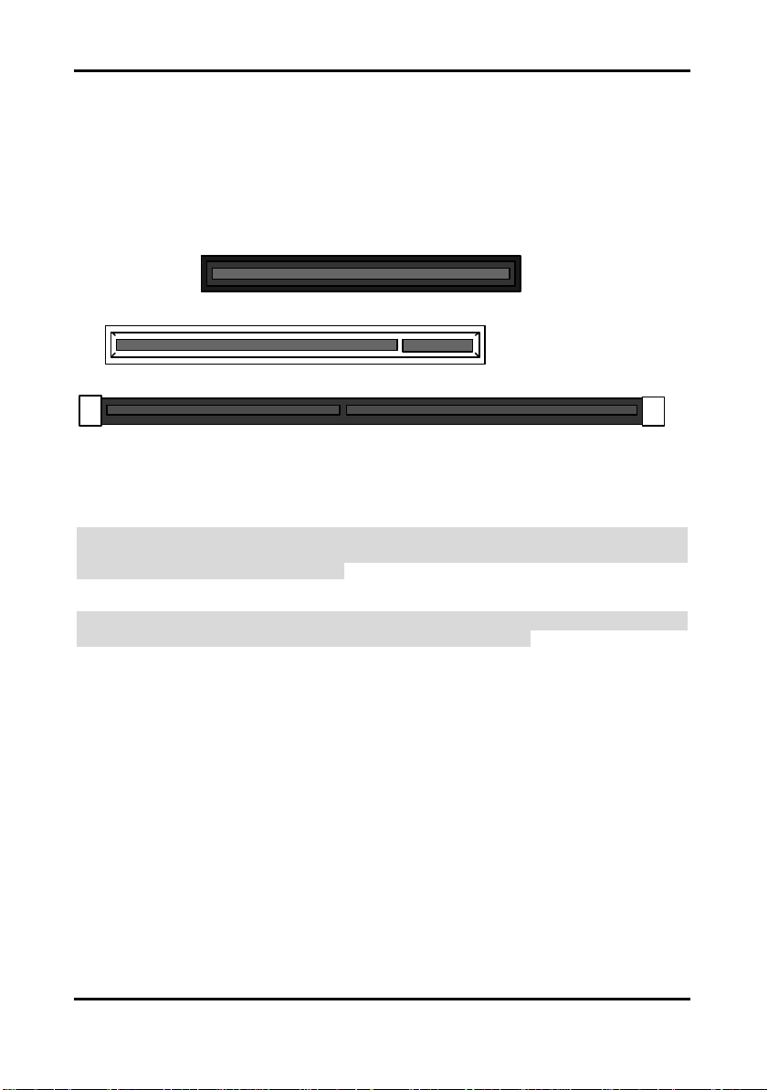
Before installing add-in cards, it’s helpful to know if they are fully compatible with your
motherboard. For this reason, we’ve provided the diagrams below, showing the most common
slots that may appear on your motherboard. Not all of the slots shown will necessarily appear
on your motherboard, however, there will be combinations of what you see here.
32 bit - 33MHz PCI Slot - 5 Volts
DDR SDRAM DIMM Slot
Simply find the appropriate slot for your add -in card and insert the card firmly. Do not force any
add-in cards (or anything else) into any slots if they won’t seat in place. It’s better to try
another slot or return the faulty card rather than damaging both the motherboard and the addin card.
TIP: It’s a good practice to install add-in cards in a staggered manner, rather than directly
adjacent to each other. This allows air to more easily circulate within the chassis, providing
improved cooling for all installed devices.
Note: YOU MUST unplug the power connector to the motherboard before performing system
hardware changes, to avoid damaging the board or expansion device.
2-20
http://www.tyan.com
Page 26
Trinity KT400 S2495 Chapter 2: Board Installation
USB2.0 Ports
COM1
COM2
USB2.0 Ports
Line-Out
Ethernet Port
S2495
1
1
KB1
USB1
COM1
COM2
LPT1
FAN1
ATX1
VIA KT400
ATX1
Connect ATX 20-pin
2.11 – Connecting External Devices
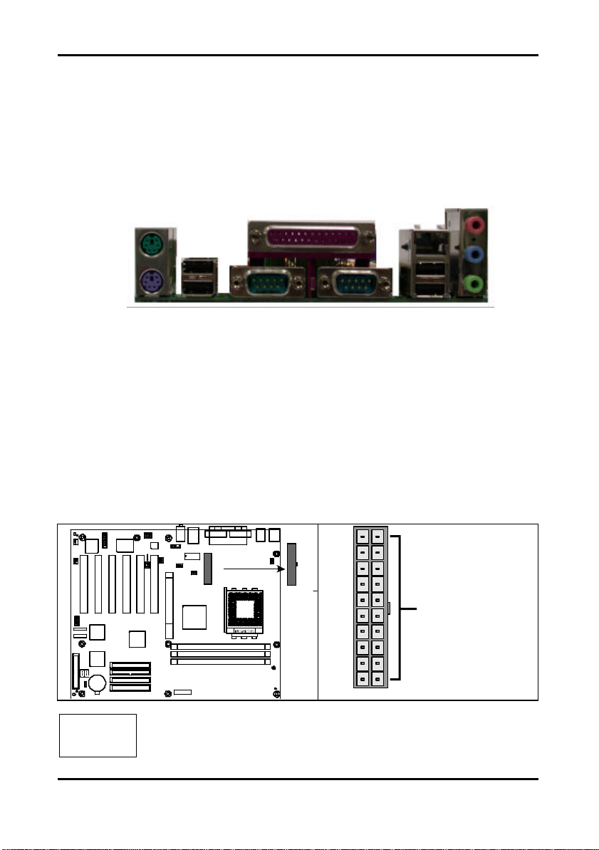
Connecting external devices to the motherboard is an easy task. The standard devices you
should expect to plug into the motherboard are keyboards, mice, and printer cables. The
following diagram will detail the ATX port stack for the following board:
Trinity KT400 S2495
Parallel Port
10/100Mbit
MIC-In
PS/2 Mouse
Line-In
PS/2 Keyboard
Besides being used primarily to connect printers, the Printer Port is also used for devices such
as Zip drive, some external CD-RW drives and or other external devices. More on the
uncommon side these days are the Serial Ports. They were primarily used to connect external
modems, but most modems today are using USB or are installed internally.
TIP: While the ports have been created to accept connectors in only one direction, make sure
to be careful when inserting connectors. At times, attaching connectors in the incorrect
orientation can damage, bend and or break the pins.
2.12 – Installing the Power Supply
The Trinity KT400 S2495 has a single 20-pin connector for ATX power supplies.
(Optional)
(Optional)
WOL
1
FAN2
1
USB3
SATA2
SATA1
FDD
LED2
1
CMOS
NOTE
1
BIOS
GAME1
SII3112
(Optional)
HPT372N
(Optional)
BAT1
1
CD1
USB2AUD2
AUX1
1
ALC650
W83697HF
PRI-IDE
SEC-IDE
RAID IDE2
RAID IDE1
1
AUD1
SPDIF1
VIA
VT8235
VT6103
FAN3
1
JCK1
1
AGP1
JCK2
PCI1PCI2PCI3PCI4PCI5PCI6
VT8377
(Optional)
(Optional)
J1
CPU
DIMM1
DIMM2
DIMM3
LED1
connector here
YOU MUST unplug the power supply before plugging the 20-pin cables to
motherboard connectors.
2-21
http://www.tyan.com
Page 27

Trinity KT400 S2495 Chapter 2: Board Installation
2.13 – Finishing Up
Congratulations on making it this far! You’re finished setting up the hardware aspect of your
computer. Before closing up your chassis, make sure that all cables and wires are connected
properly, especially IDE cables and most importantly, jumpers. You may have difficulty
powering on your system if the motherboard jumpers are not set correctly.
In the rare circumstance that you have experienced difficulty, you can find help by asking your
vendor for assistance. If they are not available for assistance, please find setup information
and documentation online at our website or by calling your vendor’s support line.
2-22
http://www.tyan.com
Page 28

Trinity KT400 S2495 Chapter 3: BIOS Setup
Chapter 3: BIOS Setup
Installation
The BIOS is the basic input/output system, the firmware on the motherboard that enables your
hardware to interface with your software. This chapter describes different settings for the
BIOS that can be used to configure your system.
The BIOS section of this manual is subject to change without notice and is provided for
reference purposes only. The settings and configurations of the BIOS are current at the time
of print, and therefore may not match exactly what is displayed on screen.
This section describes the BIOS setup program. The setup program lets you modify basic
configuration settings. The settings are then stored in a dedicated, battery-backed memory
(called NVRAM) that retains the information when the power is turned off.
This motherboard’s BIOS is a customized version of the industry -standard BIOS for IBM PC
AT-compatible personal computers. The BIOS provides critical, low-level support for the
system’s central processing unit (CPU), memory, and I/O subsystems.
This BIOS has been customized by adding important features such as virus and password
protection, power management, and chipset “tuning” features that control the system. This
section will guide you through the process of configuring the BIOS for your system setup.
Starting Setup
The BIOS is immediately activated when you turn on the computer. The BIOS reads system
configuration in CMOS RAM and begins the process of checking out the system and
configuring it through the Power-On-Self-Test (POST).
When these preliminary tests are complete, the BIOS searches for an operating system on
one of the system’s data storage devices (hard drive, CD-ROM, etc). If one is found, the BIOS
will launch that operating system and hand control over to it. You can enter the BIOS setup by
pressing the [Delete] key when the machine boots up and begins to show the memory count.
Setup Basics
The table below shows how to navigate in the setup program using the keyboard.
Tab Moves from one selection to the next
Left/Right Arrow Keys Change from one menu to the next
Up/Down Arrow Keys More between selections
Enter Opens highlighted section
PgUp/PgDn Keys Change settings.
Key Function
3-1
http://www.tyan.com
Page 29

Trinity KT400 S2495 Chapter 3: BIOS Setup
Getting Help
Pressing [F1] will display a small help window that describes the appropriate keys to use and
the possible selections for the highlighted item. To exit the Help Window, press [ESC] or the
[F1] key again.
In Case of Problems
If you discover that you have trouble booting the computer after making and saving the
changes with the BIOS setup program, you can restart the computer by holding the power
button down until the computer shuts off (usually within 4 seconds); resetting by pressing
CTRL-ALT-DEL; or clearing the CMOS.
The best advice is to only alter settings that you thoroughly understand. In particular, do not
change settings in the Chipset section unless you are absolutely sure of the outcome. The
Chipset defaults were carefully chosen by TYAN or your system manufacturer for the best
performance and reliability. Even a seemingly small change to the Chipset setup options may
cause the system to become unstable or unusable.
Setup Variations
Not all systems will have the same BIOS setup layout or options. While the basic look and
function of the BIOS setup remains more or less the s ame for most systems, the appearance
of your Setup screen may differ from the charts shown in this section. Each system design
and chipset combination requires a custom configuration. In addition, the final appearance of
the Setup program depends on the system designer. Your system designer may decide that
certain items should not be available for user configuration, and remove them from the BIOS
setup program.
NOTE: On the following pages, options written in bold type represent the BIOS Setup default.
3-2
http://www.tyan.com
Page 30
Trinity KT400 S2495 Chapter 3: BIOS Setup
3.1 – Main BIOS Setup
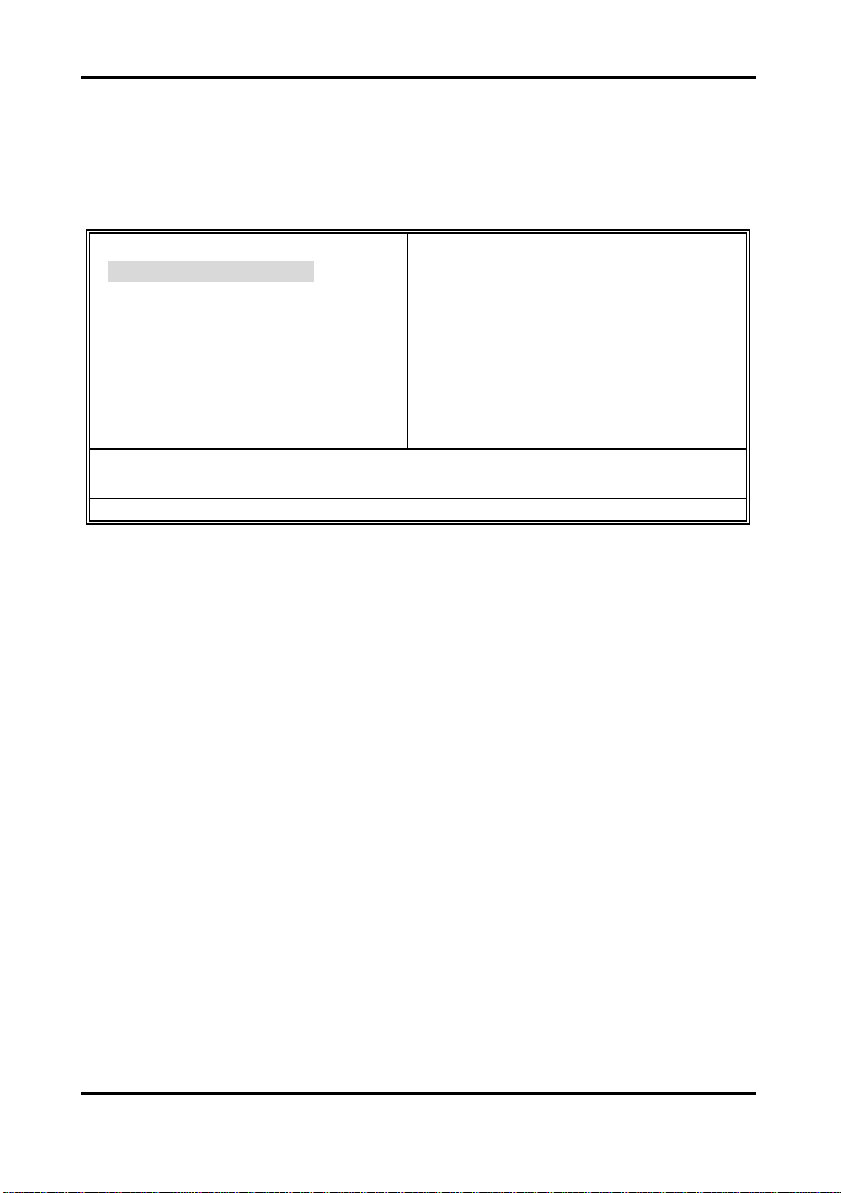
When you enter Phoenix - AwardBIOS CMOS Setup Utility, the following screen will appear as
below:
Phoenix – AwardBIOS CMOS Setup Utility
? Standard CMOS Features
? Advanced BIOS Features
? Advanced Chipset Features
? Integrated Peripherals
? Power Management Setup
? PnP/PCI Configurations
? PC Health Status
Esc: Quit ↑ ↓ ← →: Select Item
F10: Save & Exit Setup
Time, Date, Hard Disk Type…
Standard CMOS Features
Use this menu for basic system configuration.
Advanced BIOS Features
Use this menu to set the Advanced Features available on your system.
Advanced Chipset Features
Use this menu to change the values in the chipset registers and optimize your system's
performance.
Integrated Peripherals
Use this menu to specify your settings for integrated peripherals.
Power Management Setup
Use this menu to specify your settings for power management.
PnP / PCI Configuration
This entry appears if your system supports PnP / PCI.
PC Health Status
Use this menu to show your system temperature, speed and voltage status.
Frequency/Voltage Control
Use this menu to specify your settings for frequency/voltage control.
Load Fail-Safe Defaults
Use this menu to load the BIOS default values for the minimal/stable performance for your
system to operate.
? Frequency/Voltage Control
Load Fail-Safe Defaults
Load Optimized Defaults
Set Supervisor Password
Set User Password
Save & Exit Setup
Exit Without Saving
3-3
http://www.tyan.com
Page 31

Trinity KT400 S2495 Chapter 3: BIOS Setup
Load Optimized Defaults
Use this menu to load the BIOS default values that are factory settings for optimal
performance system operations. While Award has designed the custom BIOS to maximize
performance, the factory has the right to change these defaults to meet their needs.
Supervisor / User Password
Use this menu to set User and Supervisor Passwords.
Save & Exit Setup
Save CMOS value changes to CMOS and exit setup.
Exit Without Save
Abandon all CMOS value changes and exit setup.
3-4
http://www.tyan.com
Page 32

Trinity KT400 S2495 Chapter 3: BIOS Setup
year
3.2 – Standard CMOS Features
In this section, you can alter general features such as the date and time, as well as access to
the IDE configuration options. Note that the options listed below are for options that can
directly be changed within the Main Setup screen. User can Use the arrow keys to highlight
the item and then use the <PgUp> or <PgDn> keys to select the value you want in each item.
Phoenix – AwardBIOS CMOS Setup Utility
Standard CMOS Features
Date (mm: dd: yy)
Time (hh: mm: ss)
? IDE Primary Master
? IDE Primary Slave
? IDE Secondary Master
? IDE Secondary Slave
Drive A
Drive B
Video
Halt On
Based Memory
Extended Memory
Total Memory
↑↓←→: Move
Date / Time Setup:
System Date: Adjusts the system date.
MM Months
DD Days
YYYY Years
System Time: Adjusts the system clock.
HH Hours (24hr. format)
MM Minutes
SS Seconds
IDE Master / Slave Setup:
Computer detects IDE drive type from drive C to drive F.
None / Auto / Manual
Enter: Select
F5: Previous Values
Tue, Oct 1 2002
17:36:22
[2557MB]
[None]
[None]
[None]
[1.44M, 3.5 in.]
[None]
[EGA/VGA]
[All, But Keyboard]
640K
64512K
65536K
+/-/PU/PD: Value
F6: Fail-Safe Defaults
F10: Save
_________________________
Menu Level ?
Change the day, month,
and century
ESC: Exit
F7: Optimized Defaults
Item Help
F1: General Help
3-5
http://www.tyan.com
Page 33

Trinity KT400 S2495 Chapter 3: BIOS Setup
Drive A / B:
Defines the floppy drive type.
None / 360K, 5.25in / 1.2M, 5.25in / 720K, 3.5in / 1.44M, 3.5in / 2.88M, 3.5in
Video:
Defines video display mode.
EGA/VGA / CGA 40 / CGA 80 / MONO
Halt On:
Determines if the computer should stop when an error is detected during power up.
No Errors / All Errors / All, But Keyboard / All, But Diskette / All, But Disk/Key
3-6
http://www.tyan.com
Page 34
Trinity KT400 S2495 Chapter 3: BIOS Setup
Allow you to choose the VIRUS
3.3 – Advanced BIOS Feature s
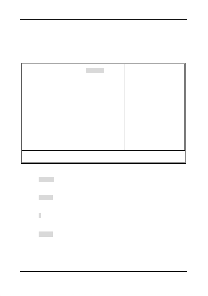
In Advanced BIOS features, you will be able to adjust many of the feature that effect system
speed and boot-up options.
Phoenix – AwardBIOS CMOS Setup Utility
Advanced BIOS Features
Virus Warning
CPU L2 Cache ECC Checking
Processor Number Feature
Quick Power On Self Test
? Boot Sequence
Swap Floppy Drive
Boot Up Floppy Seek
Boot Up NumLock Status
Gate A20 Option
Typematic Rate Setting
X Typematic Rate (Chars/Sec)
X Typematic Delay (Msec)
Security Option
APIC Mode
MPS Version Control For OS
OS Select For DRAM > 64MB
Small Logo (EPA) Show
↑↓←→: Move
Virus Warning:
This settings toggles virus protection on or off for boot sector writes.
Disabled / Auto
CPU L1 & L2 Cache:
Toggles the use of CPU L1 and L2 cache.
Enabled / Disabled
Processor Number Feature:
This option allows you to enabled or disabled the Processor Number feature.
Enabled / Dis abled
Quick Power On Self Test :
This option allows the system to skip self tests for faster startup.
Enabled / Disabled
Enter: Select
F5: Previous Values
[Disabled]
[Enabled]
[Enabled]
[Enabled]
[Press Enter]
[Disabled]
[Disabled]
[On]
[Fast]
[Disabled]
6
250
[Setup]
[Enabled]
[1.4]
[Non-OS2]
[Disabled]
+/-/PU/PD: Value
F6: Fail-Safe Defaults
F10: Save
_________________________
Menu Level ?
warning feature for IDE Hard
Disk boot sector protection. If
this function is enabled and
someone attempt to write data
into this area, BIOS will show a
warning message on screen and
alarm beep
ESC: Exit
F7: Optimized Defaults
Item Help
F1: General Help
3-7
http://www.tyan.com
Page 35
Trinity KT400 S2495 Chapter 3: BIOS Setup
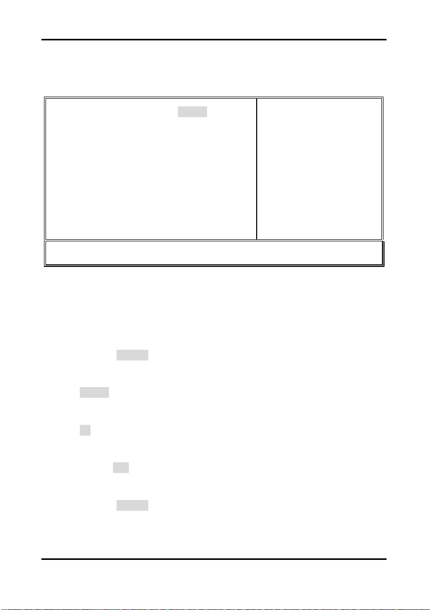
Boot Sequence:
Phoenix – AwardBIOS CMOS Setup Utility
Boot Sequence
First Boot Device
Second Boot Device
Third Boot Device
Boot Other Device
↑↓←→: Move
First / Second / Third / Other Boot Device:
This BIOS attempts to load the operating system from the devices in the sequence selected in
these item.
Swap Floppy Drive:
This option switches A: to B: drive.
Enabled / Disabled
Boot Up Floppy Seek:
This option causes the floppy drives to be detected at startup.
Enabled / Disabled
Boot Up NumLock Status:
Sets the Num Lock on or off.
On / Off
Gate A20 Option:
Leave as default.
Normal / Fast
Typematic Rate Setting:
Toggles control of keyboard key repeat rate.
Enabled / Disabled
Enter: Select
F5: Previous Values
Floppy / LS120 / HDD-0 / SCSI / CDROM / HDD-1, HDD-2 / HDD-3 / ZIP100 / USBFDD / USB-ZIP / USB-HDD / LAN / Disabled
[Floppy]
HDD -0
LS120
Enabled
+/-/PU/PD: Value
F6: Fail-Safe Defaults
F10: Save
_________________________
Menu Level ??
Select Your Boot Device Priority
ESC: Exit
F7: Optimized Defaults
Item Help
F1: General Help
3-8
http://www.tyan.com
Page 36

Trinity KT400 S2495 Chapter 3: BIOS Setup
Typematic Rate (Chars/Sec):
Defines how many characters are repeated per second when holding down a key on the
keyboard.
6 / 8 / 10 / 12 / 15 / 20 / 24 / 30
Typematic Delay (Msec):
Defines the delay that occurs at keystroke before that key will start to repeat.
250 / 500 / 750/ 1000
Security Option:
Sets the password on either just the BIOS setup or the entire system (BIOS setup included).
Setup / System
APIC Mode:
This option allows you to enabled or disabled Advanced Programmable Interrupt Controller
(APIC) Mode.
Enabled / Disabled
MPS Version Control For OS:
Selects Multi Processor specification V1.4 or V1.2.
1.4 / 1.2
OS Select For DRAM > 64MB:
Select OS2 only if you are running OS/2 operating system with more than 64MB of RAM.
Non-OS2 / OS2
Small Logo (EPA) Show:
Toggles the display of the EPA Energy Star logo at POST.
Enabled / Disabled
3-9
http://www.tyan.com
Page 37

Trinity KT400 S2495 Chapter 3: BIOS Setup
3.4 – Advanced Chipsets Features
In Advanced Chipset Features, you will be abled to adjust many of the chipset special features.
Phoenix – AwardBIOS CMOS Setup Utility
Advanced Chipset Features
? DRAM Clock / Drive Control
? AGP & P2P Bridge Control
? CPU & PCI Bus Control
System BIOS Cacheable
Video RAM Cacheable
↑↓←→: Move
DRAM Clock / Drive Control:
DRAM Timing
X DRAM CAS Latency
X Bank Interleave
X Precharge to Active (Trp)
X Active to Precharge (Tras)
X Active to CMD (Trcd)
DRAM Burst Length
DRAM Queue Depth
DRAM Command Rate
Write Recovery Time
DRAM tWTR
↑↓←→: Move
Enter: Select
F5: Previous Values
Phoenix – AwardBIOS CMOS Setup Utility
Enter: Select
F5: Previous Values
[Press Enter]
[Press Enter]
[Press Enter]
[Disabled]
[Disabled]
+/-/PU/PD: Value
F6: Fail-Safe Defaults
DRAM Clock / Drive Control
[Auto By SPD]
2.5
Disabled
3T
6T
3T
[4]
[4 level]
[2T Command]
[3T]
[3T]
+/-/PU/PD: Value
F6: Fail-Safe Defaults
F10: Save
F10: Save
_________________________
Menu Level ?
ESC: Exit
F7: Optimized Defaults
_________________________
Menu Level ??
ESC: Exit
F7: Optimized Defaults
Item Help
F1: General Help
Item Help
F1: General Help
3-10
http://www.tyan.com
Page 38

Trinity KT400 S2495 Chapter 3: BIOS Setup
DRAM Timing:
Select SPD for setting SDRAM timing by SPD.
Manual / Auto By SPD
DRAM CAS Latency:
This setting defines the number of cycles after a read command until output starts.
2 / 2.5 / 3
Bank Interleave:
The item allows to increase memory performance by interleaving the memory chip-internal
banks.
Precharge to Active (Trp):
Setup the minimum row precharge time.
2T / 3T
Active to Precharge (Tras):
Setup the minimum RAS pulse width.
5T / 6T
Active to CMD (Trcd):
Setup the minimum CAS to RAS delay.
2T / 3T
DRAM Command Rate:
Specifies the chipset latency needed to decode memory addresses and commands. With
higher system memory configurations or when Registered DIMMs are used, this item needs to
be set to 2T.
1T Command / 2T Command
2 Bank / 4 Bank / Disabled
3-11
http://www.tyan.com
Page 39
Trinity KT400 S2495 Chapter 3: BIOS Setup
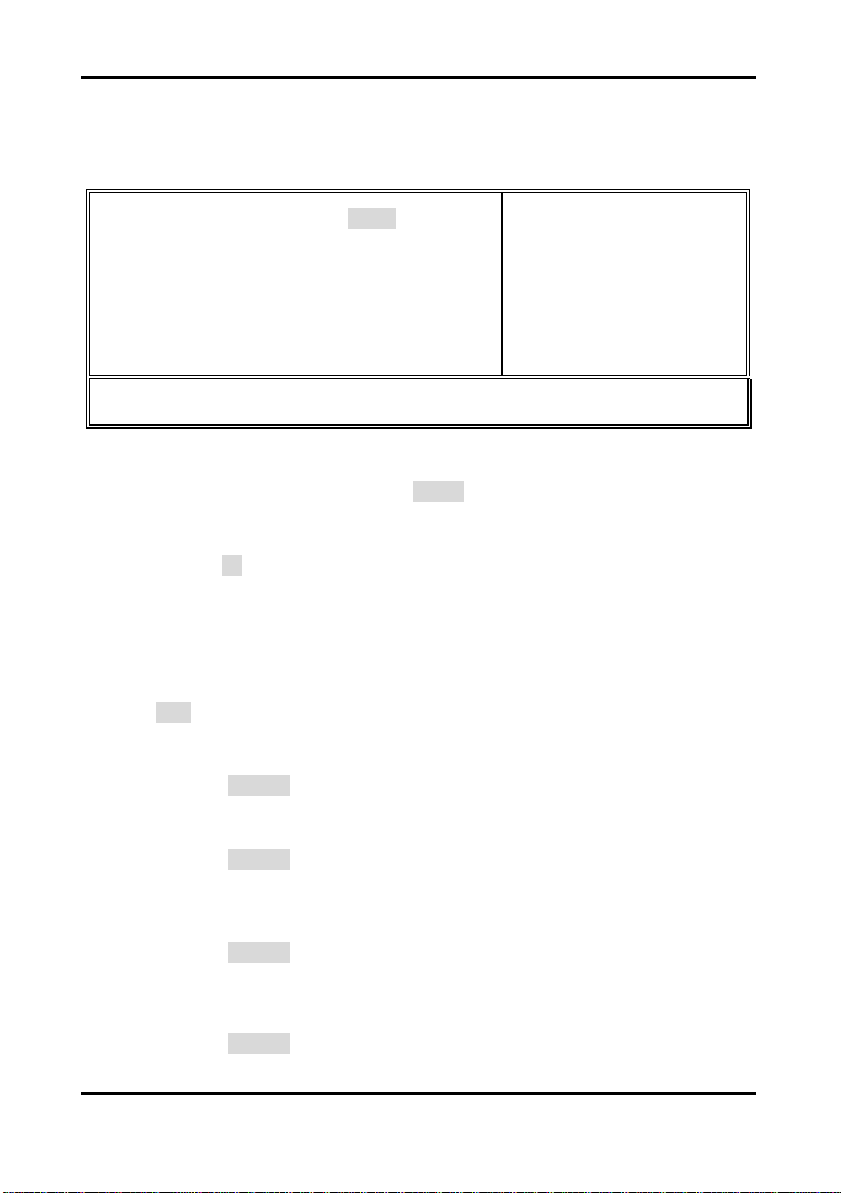
AGP & P2P Bridge Control:
Phoenix – AwardBIOS CMOS Setup Utility
AGP & P2P Bridge Control
AGP Aperture Size
AGP Mode
AGP Driving Control
X AGP Driving Value
AGP Fast Write
AGP Master 1 WS Write
AGP Master 1 WS Read
DBI Output for AGP Trans.
↑↓←→: Move
AGP Aperture Size:
The amount of system memory that the AGP card is allowed to share with.
4MB / 8MB / 16MB / 32MB / 64MB / 128MB / 256MB
AGP Mode:
Chipset AGP Mode support.
1X / 2X / 4X
If to use 8x mode AGP card, the AGP mode already lock at 8x mode, that’s why there’s no
1x/2x/4x select item on it.
AGP Driving Control:
This item allows you to adjust the AGP driving force. Choose Manual to key in an AGP
Driving Value in the next selection. This field recommended to set “Auto” for avoiding any
error in your system.
Auto
AGP Fast Write:
Enables writes to AGP directly from memory bypassing the CPU in AGP4X and 8X .
Enabled / Disabled
AGP Master 1 WS Write:
When “Enabled”, Write to the AGP are executed with one waiting states.
Enabled / Disabled
AGP Master 1 WS Read:
The default is 2T, enabling 1T can increase the performance but also introduce stability
problems.
Enabled / Disabled
DBI Output for AGP:
Dynamic Bus Inversion(DBI) reduces simultaneously switching output(SSO) noise and
increases stability and signal integrity(only available with AGP 8X cards)
Enabled / Disabled
Enter: Select
F5: Previous Values
[128M]
[4X]
[Auto]
DA
[Disabled]
[Disabled]
[Disabled]
[Disabled]
+/-/PU/PD: Value
F6: Fail-Safe Defaults
F10: Save
_________________________
Menu Level ??
ESC: Exit
F7: Optimized Defaults
Item Help
F1: General Help
3-12
http://www.tyan.com
Page 40
Trinity KT400 S2495 Chapter 3: BIOS Setup
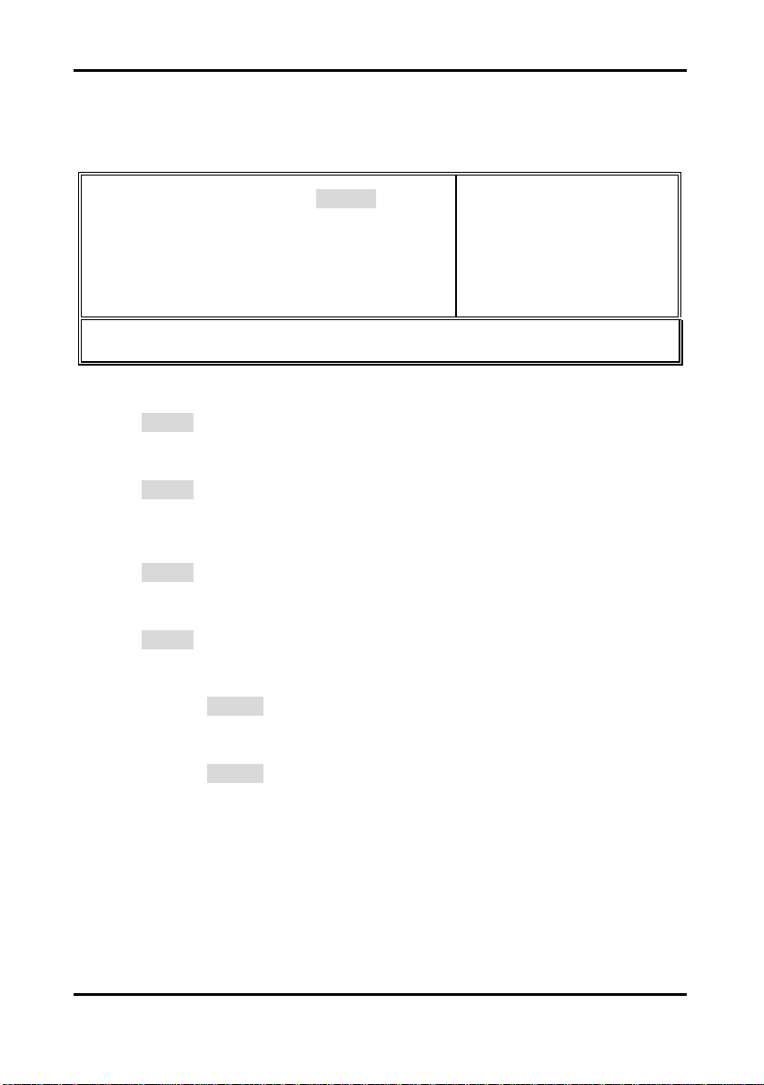
CPU & PCI Bus Control:
Phoenix – AwardBIOS CMOS Setup Utility
CPU & PCI Bus Control
PCI1 Master 0 WS Write
PCI2 Master 0 WS Write
PCI1 Post Write
PCI2 Post Write
VLink 8X Support
PCI Delay Transaction
[Enabled]
[Enabled]
[Enabled]]
[Enabled]
[[Enabled]
[Enabled]
Item Help
_________________________
Menu Level ??
↑↓←→: Move
PCI1 Master 0 WS Write:
When “Enabled”, Write to the PCI1 bus is commanded with zero waiting states.
Enabled / Disabled
PCI2 Master 0 WS Write:
When “Enabled”, Write to the PCI2 bus is commanded with zero waiting states.
Enabled / Disabled
PCI Delay Transaction:
The chipset has an embedded 32-bit posted write buffer to suppor t delay transactions cycles.
Select “Enabled” to support compliance with PCI specification version 2.1
Enabled / Disabled
VLink 8X Support:
Enables 533Mbytes/sec connection between South and Northbridge.
Enabled / Disabled
System BIOS Cacheable:
This option allows you to copy your BIOS code from slow ROM to fast RAM.
Enabled / Disabled
Video RAM Cacheable:
This option allows the CPU to cache read / write of the video RAM. Leave as default.
Enabled / Disabled
Enter: Select
F5: Previous Values
+/-/PU/PD: Value
F6: Fail-Safe Defaults
F10: Save
ESC: Exit
F7: Optimized Defaults
F1: General Help
3-13
http://www.tyan.com
Page 41

Trinity KT400 S2495 Chapter 3: BIOS Setup
3.5 – Integrated Peripherals
Options related to onboard peripheral features can be altered through the following:
Phoenix – AwardBIOS CMOS Setup Utility
Integrated Peripherals
? VIA OnChip IDE Device
? PCI Device Setup
? Super IO Device
Init Display First
↑↓←→: Move
VIA OnChip IDE Device:
OnChip IDE Channel0
OnChip IDE Channel1
IDE Prefetch Mode
Primary Master PIO
Primary Slave PIO
Secondary Master PIO
Secondary Slave PIO
Primary Master UDMA
Primary Slave UDMA
Secondary Master UDMA
Secondary Slave UDMA
IDE HDD Block Mode
HDD S.M.A.R.T. Capability
↑↓←→: Move
Enter: Select
F5: Previous Values
Enter: Select
F5: Previous Values
Phoenix – AwardBIOS CMOS Setup Utility
[Press Enter]
[Press Enter]
[Press Enter]
[PCI Slot]
+/-/PU/PD: Value
F6: Fail-Safe Defaults
VIA OnChip IDE Device
[Enabled]
[Enabled]
[Enabled]
[Auto]
[Auto]
[Auto]
[Auto]
[Auto]
[Auto]
[Auto]
[Auto]
[Enabled]
[Disabled]
+/-/PU/PD: Value
F6: Fail-Safe Defaults
F10: Save
F10: Save
_________________________
Menu Level ?
ESC: Exit
F7: Optimized Defaults
_________________________
Menu Level ??
ESC: Exit
F7: Optimized Defaults
Item Help
F1: General Help
Item Help
F1: General Help
3-14
http://www.tyan.com
Page 42
Trinity KT400 S2495 Chapter 3: BIOS Setup
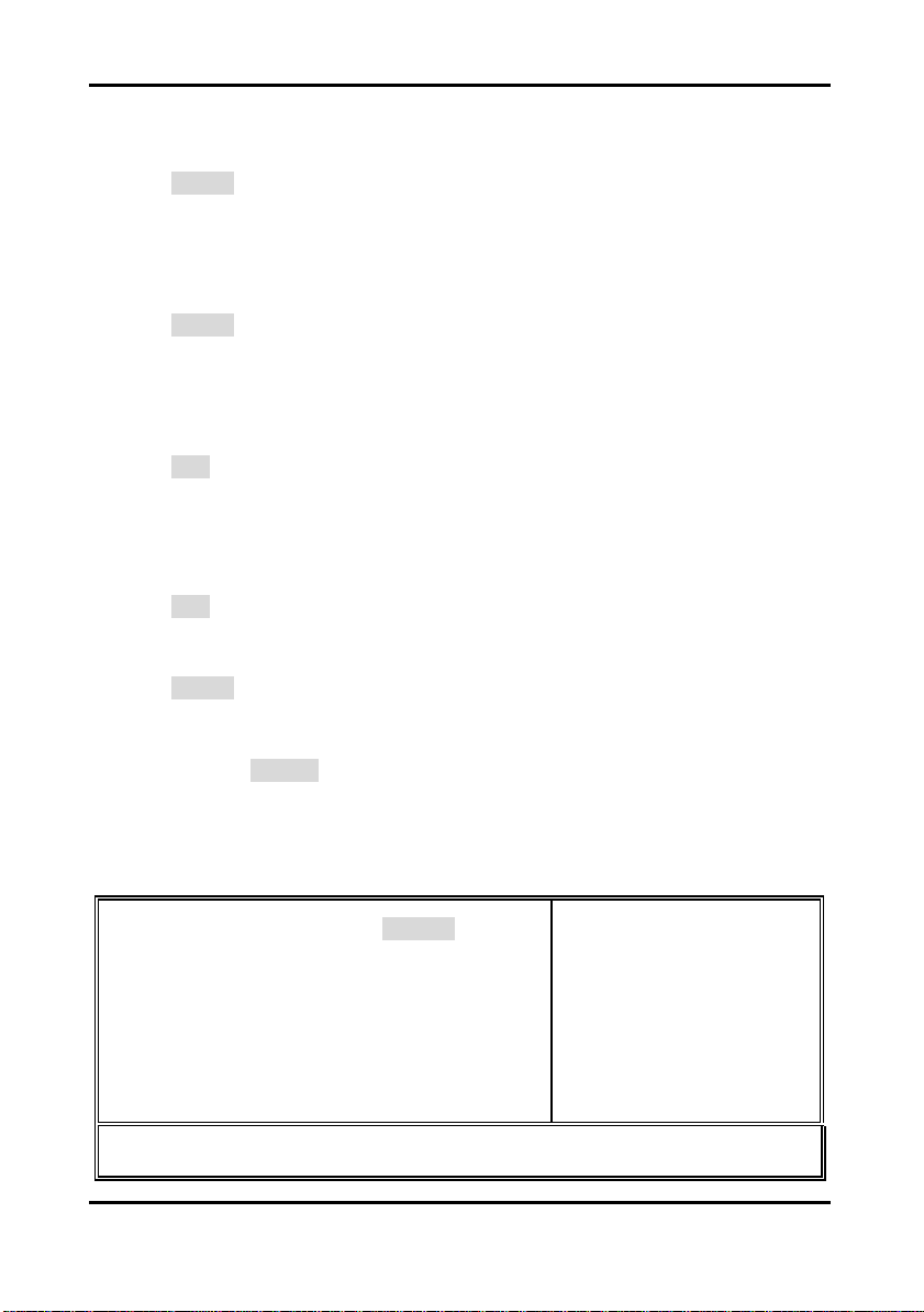
OnChip IDE Channel0 / 1:
The integrated peripheral controller contains an IDE interface with support for two IDE
channels. Select “Enabled” to activate each channel separately.
Enabled / Disabled
IDE Prefetch Mode:
Enabled prefetching for IDE drive interfaces that support its faster drive accesses. If you are
getting disk drive errors, change the setting to omit the drive interface where the errors occur.
Depending on the configuration of your IDE subsystem, this field may not appear, and it does
not appear when the Internal PCI / IDE field, above, is Disabled.
Enabled / Disabled
Primary / Secondary Master/ Slave PIO:
The four IDE PIO (Programmed Input / Output) field let you set a PIO mode (0-4) for each of
the four IDE devices that the onboard IDE interface supports. Modes 0 through 4 provide
successively increased performance. In Auto mode, the system automatically determines the
best mode for each device.
Auto / Mode 0 / Mode 1 / Mode 2 / Mode 3 / Mode 4
Primary / Secondary Master/ Slave UDMA:
This allows you to select the mode of operation for the Ultra DMA/33 implementation is
possible only if your IDE hard drive supports it and the operating environment includes a DMA
driver (Windows 95 OSR2 or a third-party IDE bus master driver). If your hard drive and your
system software both support Ultra DMA/33, select Auto to enable bios SUPPORT.
Auto / Disabled
IDE HDD Block Mode:
Leave this setting as is.
Enabled / Disabled
HDD S.M.A.R.T. Capability:
Allow you to choose the HDD S.M.A.R.T. for detect HDD CONDITION.
Enabled / Disabled
PCI Device Setup:
Phoenix – AwardBIOS CMOS Setup Utility
PCI Device Setup
USB 2.0 Support
AC97Audio
OnChip LAN
Onboard Lan Boot ROM
OnChip USB Controller
USB Keyboard Support
USB Mouse Support
Onboard RAID IDE Device
Onboard SATA IDE Device
↑↓←→: Move
Enter: Select
F5: Previous Values
[Enabled]
[Auto]
[Enabled]
[Disabled]
[All Enabled]
[Disabled]
[Disabled]
[Enabled]
[Enabled]
+/-/PU/PD: Value
F6: Fail-Safe Defaults
3-15
http://www.tyan.com
F10: Save
_________________________
Menu Level ??
ESC: Exit
F7: Optimized Defaults
Item Help
F1: General Help
Page 43
Trinity KT400 S2495 Chapter 3: BIOS Setup
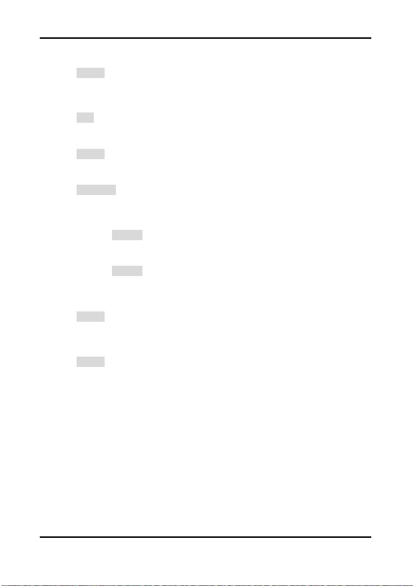
USB 2.0 Support:
This item allows you to decide to “Enable” or “Disable” the USB 2.0 device.
Enabled / Disabled
AC97Audio:
This item allows you to decide to Audio / disable the chipset family to support AC97 Audio.
The function is setting AC97 Audio Codec states.
Auto / Disabled
OnChip LAN:
This item allows you to “Enable” or “Disable” onboard LAN function.
Enabled / Disabled
OnChip USB Controller:
This item allows you to “Enable” or “Disable” onboard USB function.
All Enabled / All Disabled / 1&2 USB Port / 2&3 USB Port / 1&3 USB Port / 1 Port
USB Keyboard Support:
Select “Enabled” if your system contains a USB controller and you have a USB keyboard.
Enabled / Disabled
USB Mouse Support:
Select “Enabled” if your system contains a USB controller and you have a USB mouse.
Enabled / Disabled
Onboard RAID IDE Device: (Optional)
This item is optional function. It allows you to decide to “Enable” or “Disable” the onboard
RAID IDE device.
Enabled / Disabled
Onboard SATA IDE Device: (Optional)
This item is optional function. It allows you to decide to “Enable” or “Disable” the onboard
SATA (Serial ATA) device.
Enabled / Disabled
/ 2 Port / 3 Port
3-16
http://www.tyan.com
Page 44
Trinity KT400 S2495 Chapter 3: BIOS Setup
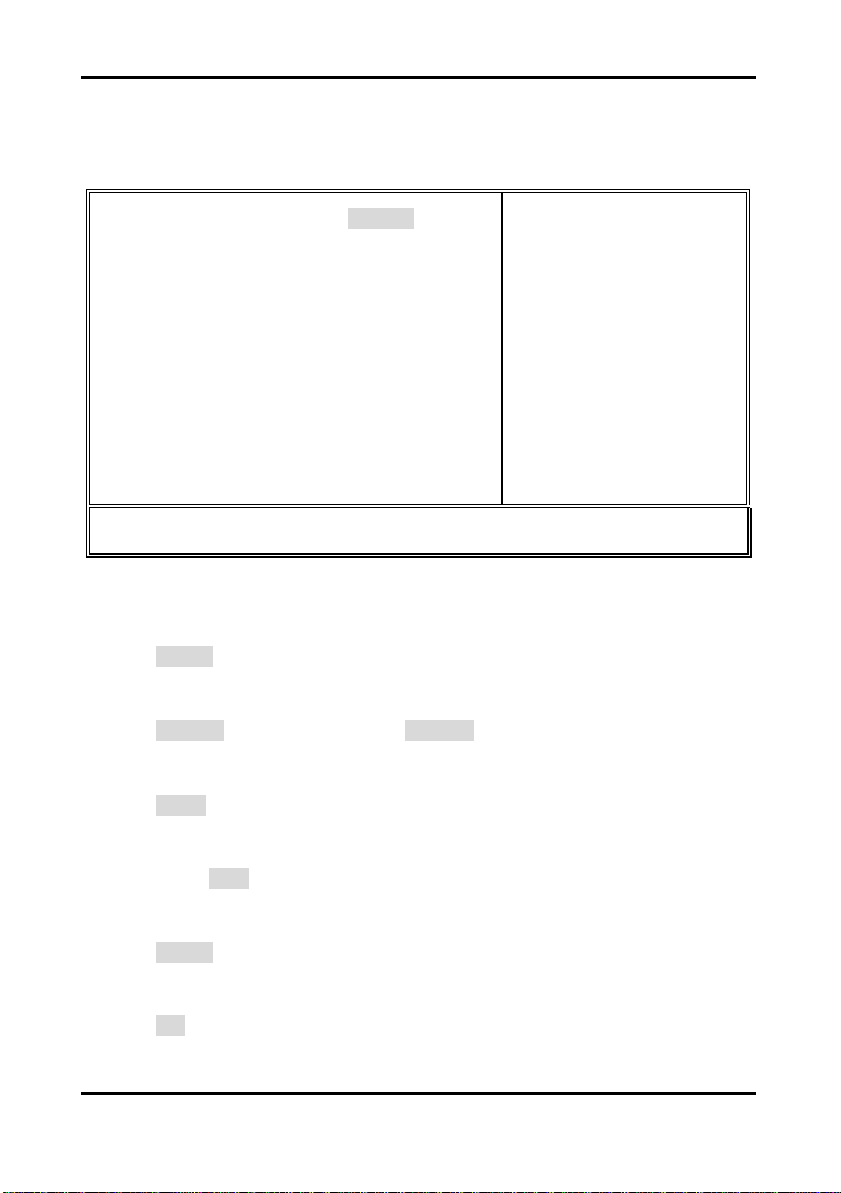
Super IO Device:
Phoenix – AwardBIOS CMOS Setup Utility
Super IO Device
Onboard FDC Controller
Onboard Serial Port 1
Onboard Serial Port 2
UART Mode Select
RxD, TxD Active
IR Transmission Delay
UR2 Duplex Mode
Use IR Pins
Onboard Parallel Port
Parallel Port Mode
EPP Mode Select
ECP Mode Use DMA
Game Port Address
Midi Port Address
X Midi Port IRQ
↑↓←→: Move
Onboard FDC Controller:
Select Enabled if your system has a floppy disk controller (FDC) installed on the system board
and you wish to use it. If you install and-in FDC or the system has no floppy drive, select
“Disabled” in the field.
Enabled / Disabled
Onboard Serial Port 1 / 2:
Select an address and corresponding interrupt for the first and second serial ports.
3F8/IRQ4 / 2E8/IRQ3 / 3E8/IRQ4 / 2F8/IRQ3 / Disabled / Auto
UART Mode Select:
This field allows the users to configure what IR mode the 2nd serial port should use.
Normal / IrDA and ASKIR
RxD, TxD Active:
This field configures the receive and transmit signals generated from the IR port.
Hi, Hi / Hi, Lo / Lo, Hi / Lo, Lo
IR Transmission Delay:
This item allows you to “Enabled” or Disabled” the IR transmission delay.
Enabled / Disabled
UR2 Duplex Mode:
This item allows you to select IR “Half” or “Full” duplex function.
Half / Full
Enter: Select
F5: Previous Values
[Enabled]
[3F8 / IRQ4]
[2F8 / IRQ3]
[Normal]
[Hi, Lo]
[Enabled]
[Half]
[IR-Rx2Tx2]
[378 / IRQ7]
[SPP]
[EPP1.7]
[3]
[201]
[Disabled]
10
+/-/PU/PD: Value
F6: Fail-Safe Defaults
F10: Save
_________________________
Menu Level ??
ESC: Exit
F7: Optimized Defaults
Item Help
F1: General Help
3-17
http://www.tyan.com
Page 45
Trinity KT400 S2495 Chapter 3: BIOS Setup
Use IR Pins:
This item allows you to select IR transmission routes, one is “RxD2, TxD2 (COM Port) and the
other is IR-Rx2Tx2.
RxD2, TxD2 / IR-Rx2Tx2
Onboard Parallel Port:
This field allows the user to configure the LPT port.
378/IRQ7 / 278/IRQ5 / 3BC/IRQ7 / Disabled
Parallel Port Mode:
This field allows the user to select the parallel port mode.
SPP / EPP / ECP / ECP+EPP
EPP Mode Select:
This item allows you to determine the IR transfer mode of onboard I/O chip.
EPP1.9 / EPP1.7
ECP Mode Use DMA:
This field allows the user to select the DMA1 or DMA3 for the ECP mode.
DMA1 / DMA3
Game Port Address:
Select an address for the Game port.
201 / 209 / Disabled
Midi Port Address:
Select an address for the MiDi port.
290 / 300 / 330 / Disabled
Midi Port IRQ:
Select an interrupt for the MiDi port.
5 / 10
3-18
http://www.tyan.com
Page 46
Trinity KT400 S2495 Chapter 3: BIOS Setup
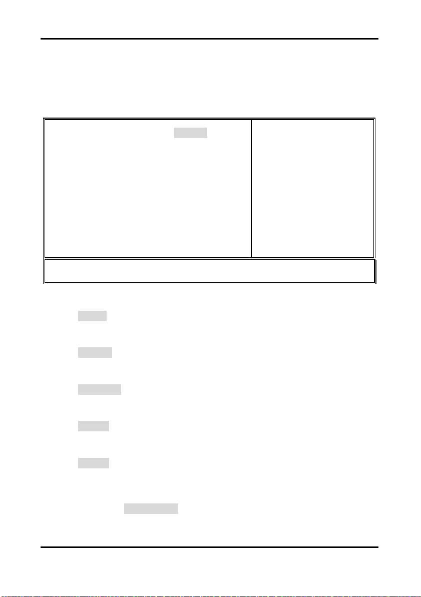
3.6 – Power Management Setup
Options related to power management can be altered through the following:
Phoenix – AwardBIOS CMOS Setup Utility
Power Management Setup
ACPI Function
ACPI Suspend Type
Power Management Option
HDD Power Down
Suspend Mode
Video Off Option
Video Off Method
MODEN Use IRQ
Soft-off by PWRBTN
Run VGABIOS if S3 Resume
States After Power Failure
? IRQ/Event Activity Detect
↑↓←→: Move
ACPI Function:
Toggles advanced power and configuration done by OS.
Enabled / Disabled
ACPI Suspend Type:
Defines ACPI system suspend mode.
S1 (POS)
Power Management Option:
Defines the type of power saving features the system should follow.
User Define / Maximum Saving / Minimum Saving
HDD Power Down:
Defines hard drive power down delay.
Disabled / 1 minutes / 5 minutes / 10 minutes / 30 minutes / 45 minutes / 60 minutes
Suspend Mode:
Defines the method used to power off the system.
Disabled / Standby / Sleep
Video Off Option:
Tell you what time frame that the video will be disabled under current power management
settings.
Always On / Suspend -> Off
Enter: Select
F5: Previous Values
[Enabled]
[S1 (POS)]
[User Define]
[Disabled]
[Disabled]
[Suspend -> off]
[V/H SYNC+Blank]
[3]
[Instant]
[Auto]
[Auto]
[Press Enter]
+/-/PU/PD: Value
F6: Fail-Safe Defaults
F10: Save
_________________________
Menu Level ?
ESC: Exit
F7: Optimized Defaults
Item Help
F1: General Help
3-19
http://www.tyan.com
Page 47
Trinity KT400 S2495 Chapter 3: BIOS Setup
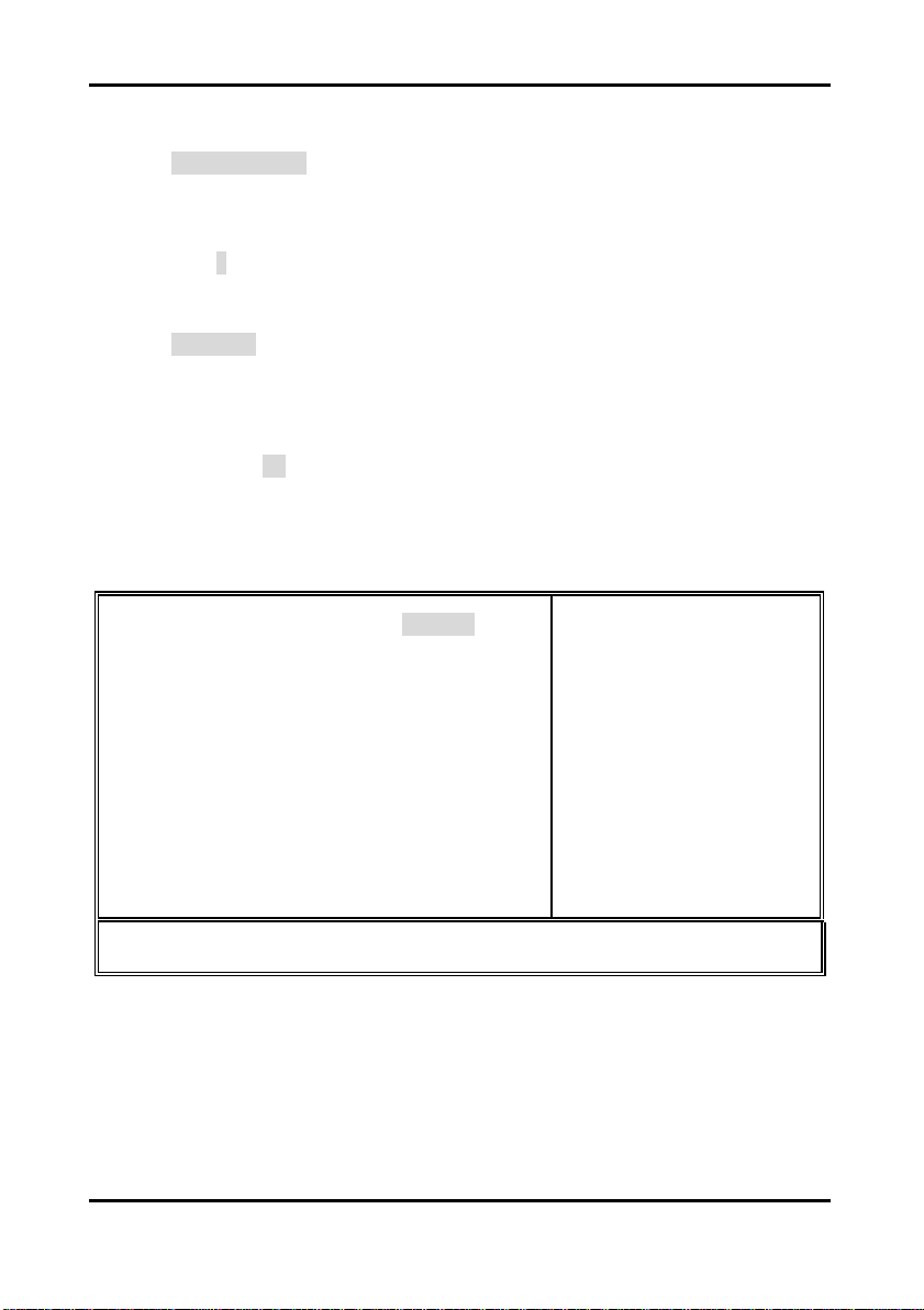
Video Off Method:
Defines the method used to power off graphics.
V/H SYNC+Blank / Blank / DPMS
MODEM Use IRQ:
Name the interrupt request (IRQ) line assigned to the modem (if any) on your system. Activity
of the selected IRQ always awakens the system.
N/A / 3 / 4 / 5 / 7 / 9 / 10 / 11
Soft-off by PWRBTN:
Defines the action of the power button when pressed.
Instant-Off / 4-seconds
States After Power Failure:
This field lets you determine the state that your PC returns to after a power failure. If set to
“Off”, the PC will not boot after a power failure, if set to “On”, the PC will restart after a power
failure.
Auto / On / Off
IRQ/Event Activity Detect:
Phoenix – AwardBIOS CMOS Setup Utility
IRQ/Event Activity Detect
PS2KB Wakeup Select
PS2KB Wakeup from S3/S4/S5
PS2MS Wakeup from S3/S4/S5
USB Resume from S3
VGA
LPT & COM
HDD & FDD
PCI Master
PowerOn by PCI Card
Wake Up On LAN / Ring
RTC Alarm Resume
X Date (of Month)
X Resume Time (hh: mm: ss)
? IRQs Activity Monitoring
↑↓←→: Move
PS2KB Wakeup Select:
This item allows you to select Hot Key or Password to wake-up the system by PS2 Keyboard.
When select Password, please press “ENTER ” key to change password max 8 numbers.
Enter: Select
F5: Previous Values
[Hot Key]
[Disabled]
[Disabled]
[Disabled]
[OFF]
[LPT / COM]
[ON]
[OFF]
[Disabled]
[Disabled]
[Disabled]
0
0: 0: 0
[Press Enter]
+/-/PU/PD: Value
F6: Fail-Safe Defaults
3-20
http://www.tyan.com
F10: Save
_________________________
Menu Level ??
When Select Password, Please
press ENTER key to change
Password Max 8 numbers.
ESC: Exit
F7: Optimized Defaults
Item Help
F1: General Help
Page 48

Trinity KT400 S2495 Chapter 3: BIOS Setup
PS2KB / MS Wakeup from S3/S4/S5:
This item allows you to set a Hot Key to wake -up the system by PS2 Keyboard.
Disabled / Ctrl+F1 / Ctrl+F2 / Ctrl+F3 / Ctrl+F4 / Ctrl+F5 / Ctrl+F6 / Ctrl+F7 / Ctrl+F8
Note: Power and Wake are the Windows98 Keyboard button.
VGA:
When set to “On”, any event occurring at a VGA port will awaken a system, which has been
powered down.
On / Off
LPT & COM:
When set to “LPT/COM”, any event occurring at a COM (serial) / LPT (printer) port will awaken
a system, which has been powered down.
LPT/COM
HDD & FDD:
When set to “On”, any event occurring at a hard or floppy drive port will awaken a system,
which has been powered down.
On / Off
PCI Master:
When set to “Off”, any event occurring to the DMA controller will awaken a system, which has
been powered down.
On / Off
PowerOn by PCI Card:
An input signal from PME on the PCI card awakens the system from a soft off state.
Enabled / Disabled
Wake Up On LAN / Ring:
Defines whether the system will wake up if the modem is dialed into.
Enabled / Disabled
RTC Alarm Resume:
Defines the time / date when the system will wake up.
Enabled / Disabled
/ Ctrl+F9 / Ctrl+F10 / Ctrl+F11 / Ctrl+F12 / Power / Wake / Any Key
3-21
http://www.tyan.com
Page 49

Trinity KT400 S2495 Chapter 3: BIOS Setup
IRQs Activity Monitoring:
Phoenix – AwardBIOS CMOS Setup Utility
IRQs Activity Monitoring
Primary INTR
IRQ3 (COM 2)
IRQ4 (COM 1)
IRQ5 (LPT 2)
IRQ6 (Floppy Disk)
IRQ7 (LPT 1)
IRQ8 (RTC Alarm)
IRQ9 (IRQ2 Redir)
IRQ10 (Reserved)
IRQ11 (Reserved)
IRQ12 (PS/2 Mouse)
IRQ13 (Coprocessor)
IRQ14 (Hard Disk)
IRQ15 (Reserved)
↑↓←→: Move
Primary INTR:
When set to “On”, any event occurring at will awaken a system which has been powered down.
On / Off
IRQs 3 ~ 15:
Allows you to set system to monitor IRQs 3 ~ 15 for activity to awaken system from a power
management mode.
Enter: Select
F5: Previous Values
[On]
[Enabled]
[Enabled]
[Enabled]
[Enabled]
[Enabled]
[Enabled]
[Enabled]
[Enabled]
[Enabled]
[Enabled]
[Enabled]
[Enabled]
[Enabled]
+/-/PU/PD: Value
F6: Fail-Safe Defaults
F10: Save
_________________________
Menu Level ???
ESC: Exit
F7: Optimized Defaults
Item Help
F1: General Help
3-22
http://www.tyan.com
Page 50
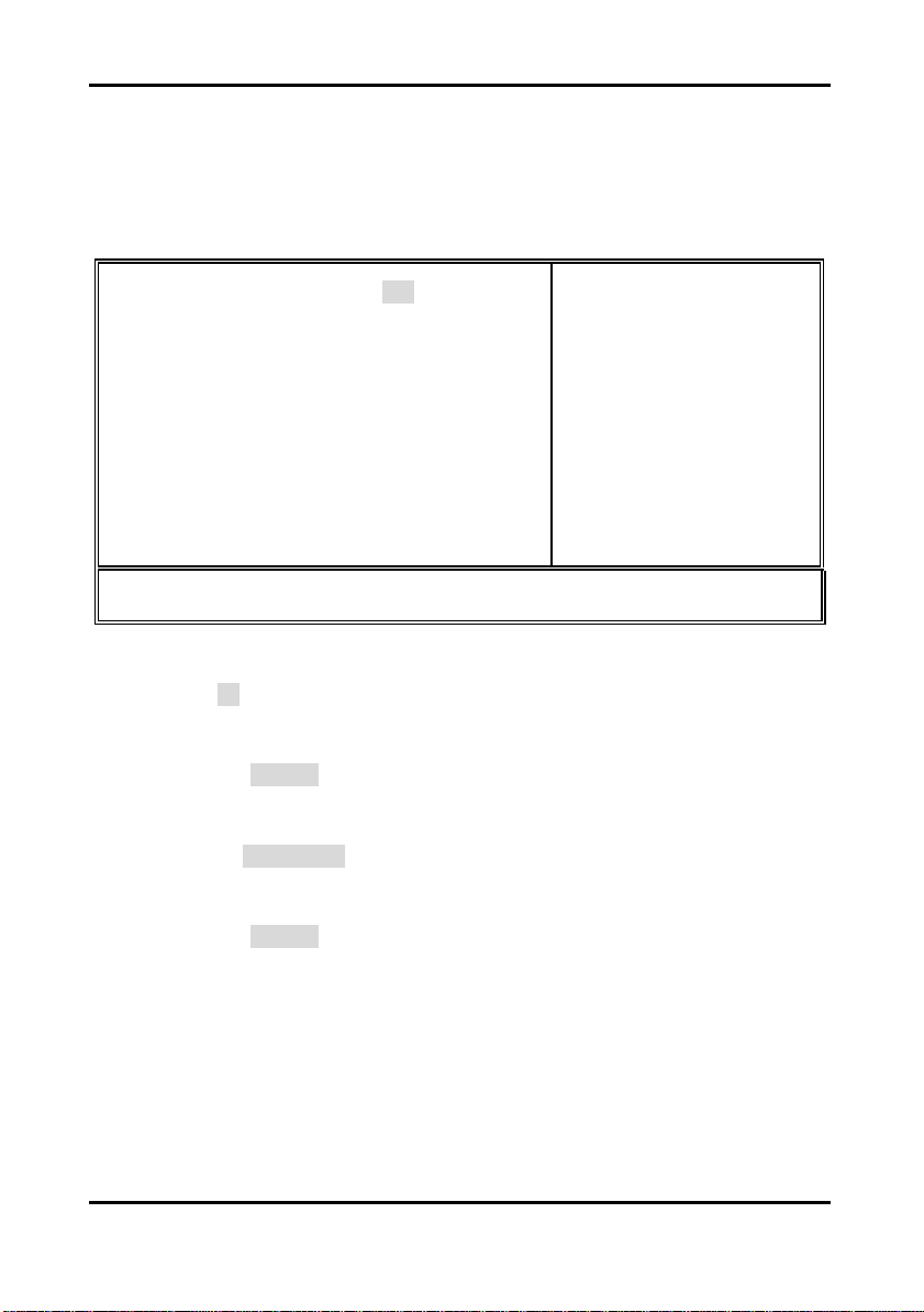
Trinity KT400 S2495 Chapter 3: BIOS Setup
3.7 – PnP/PCI Configurations
Options related to all the configurations of PnP / PCI resources.
Phoenix – AwardBIOS CMOS Setup Utility
PnP / PCI Configurations
PNP OS Installed
Reset Configuration Data
Resources Controlled By
X IRQ Resources
PCI / VGA Palette Snoop
PCI Device List
↑↓←→: Move
PNP OS Installed:
Select “Yes”, if you are using a PNP OS, otherwise select “No”.
Yes / No
Reset Configuration Data:
This setting allow you to clear ESCD data.
Enabled / Disabled
Resources Controlled By:
Default whether system resources are controller by BIOS or by user.
Manual / Auto (ESCD)
PCI / VGA Palette Snoop:
Leave as default.
Enabled / Disabled
Enter: Select
F5: Previous Values
[No]
[Disabled]
[Auto (ESCD)]
[Press Enter]
[Disabled]
[Enabled]
+/-/PU/P D: Value
F6: Fail-Safe Defaults
F10: Save
_________________________
Menu Level ?
Select Yes if you are using a
Plug and Play capable operation
system Select No if you need
the BIOS to configure n0n-boot
devices
ESC: Exit
F7: Optimized Defaults
Item Help
F1: General Help
3-23
http://www.tyan.com
Page 51
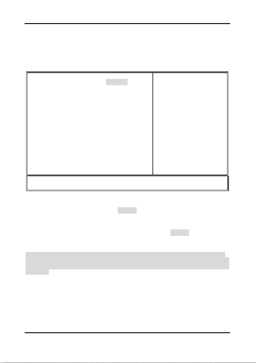
Trinity KT400 S2495 Chapter 3: BIOS Setup
3.8 – PC Health Status
This menu is related to detecting system temperature, voltage, fan and speed.
Phoenix – AwardBIOS CMOS Setup Utility
PC Health Status
CPU Warning Temperature
Current System Temp.
Current CPU Temp.
Current FAN1 Speed
Current FAN2 Speed
Vcore (V)
Vagp (V)
+ 5 V
+12 V
3.3 (V)
Vdimm (V)
VBAT (V)
5VSB (V)
Shutdown temperature
↑↓←→: Move
CPU Warning Temperature:
To set the CPU warning temperature.
50°C, 122°F / … / 70°C, 158°F / Disabled (Step by 3°C).
Shutdown temperature:
To shut down the system when temperature exceeds. [C/P]
60°C, 140°F / 65°C, 149°F / 70°C, 158°F / 75°C, 167°F / Disabled
Note: The onboard Winbond® 83697HF hardware monitoring ASIC automatically detects the
system, motherboard and CPU temperature. It detects the CPU and chassis fan speeds in
RPM. The hardware monitor ASIC also detects the voltage output through the voltage
regulators.
Enter: Select
F5: Previous Values
[Disabled]
24°C / 75°F
40°C / 104°F
5152RPM
4182RPM
1.71V
1.52V
4.81V
11.73V
3.32V
2.56V
3.02V
4.46V
[Disabled]
+/-/PU/PD: Value
F6: Fail-Safe Defaults
F10: Save
_________________________
Menu Level ?
ESC: Exit
F7: Optimized Defaults
Item Help
F1: General Help
3-24
http://www.tyan.com
Page 52
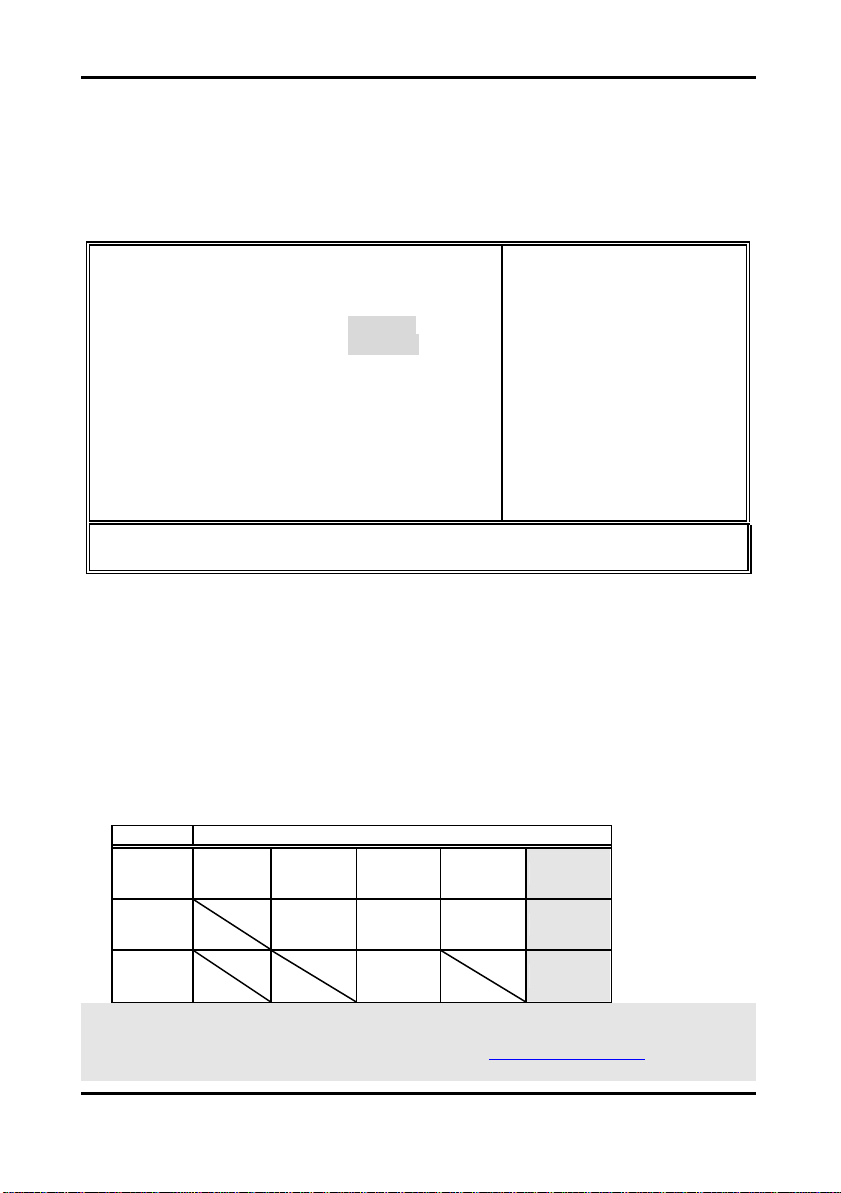
Trinity KT400 S2495 Chapter 3: BIOS Setup
3.9 – Frequency/Voltage Control
Options related to control CPU clock and frequency ratio.
Phoenix – AwardBIOS CMOS Setup Utility
Frequency / Voltage Control
Current FSB Frequency
Current DDR/AGP Frequency
Next Boot DDR/AGP Freq.
DRAM Clock
Auto Detect DIMM / PCI Clk
Spread Spectrum
CPU Clock
CPU Ratio
CPU Voltage Regulator
DIMM Voltage Regulator
↑↓←→: Move
Current FSB Frequency:
Show CPU clock frequency information.
No Option / Display Only
Current DDR/AGP Frequency:
Show DRAM frequency information
No Option / Display Only
Next Boot DDR/AGP Freq.:
This item will show DDR/AGP frequency at next time boot
No Option / Display Only
DRAM Clock:
The item will synchronize DRAM clock operation.
100MHz
133MHz
166MHz
Enter: Select
F5: Previous Values
FSB DRAM Clock Options
100MHz
(DDR200)
133MHz
(DDR266)
133MHz
(DDR266)
166MHz
[By SPD]
[Disabled]
[Disabled]
[100MHz]
[Default]
[Default]
[Default]
+/-/PU/PD: Value
F6: Fail-Safe Defaults
166MHz
*(DDR333)
166MHz
*(DDR333)
*(DDR333)
F10: Save
200MHz
*(DDR400)
200MHz
*(DDR400)
_________________________
Menu Level ?
ESC: Exit
F7: Optimized Defaults
By SPD
By SPD
By SPD
Item Help
F1: General Help
*Note: 1. When FSB is set at 166MHz the memory is only able to run at DDR333 mode.
3) support only. Please go to TYAN website http://www.TYAN.com for the latest
2. PC2700 maximum to 2 DIMM support only. PC3200 maximum to 1 DIMM (DIMM
DDR 400/PC3200 qualified memory test list.
3-25
http://www.tyan.com
Page 53
Trinity KT400 S2495 Chapter 3: BIOS Setup
Auto Detect DIMM / PCI Clk:
Sets the BIOS to automatically adjust PCI and memory bus speeds accordingly.
Enabled / Disabled
Spread Spectrum:
Reduces interference on the motherboard. Leave as default if your system works correctly.
Enabled / Disabled
CPU Clock:
Enter a decimal number to set the front side bus speed of the motherboard. For all purposes
and to maintain stability, please keep this setting at its default setting.
100MHz, If JCK1 and JCK2 are both at 1-2,
133MHz, If JCK1 and JCK2 are at 2-3 and 1-2 respectively
or 166MHz, If JCK1 and JCK2 are both at 2-3.
CPU Ratio:
Sets the CPU multiplier. TYAN does not recommend changing this setting from the default
setting.
16X… 22X / Auto / Default
CPU Voltage Regulator:
This option allows you to change the default core voltage of the processor. Please always
leave at default settings.
Default
DIMM Voltage Regulator:
This option allows you to change the default core voltage of the DIMM memory. Please
al ways leave at default settings.
Default
3.10 – Load Fail-Safe Defaults
When you press <Enter> on this item you get a confirmation dialog box with a message similar
to:
Pressing ‘Y’ loads the BIOS default values for the most stable, minimal-performance system
operations.
Load Fail-Safe Defaults (Y/N)? N
3.11 – Load Optimized Defaults
When you press <Enter> on this item you get a confirmation dialog box with a message similar
to:
Pressing ‘Y’ loads the default values that are factory settings for optimal performance system
operations.
Load Optimized Defaults (Y/N)? N
3-26
http://www.tyan.com
Page 54

Trinity KT400 S2495 Chapter 3: BIOS Setup
3.12 – Supervisor/User Password Setting
You can set either supervisor or user password, or both of then. The differences between are:
Set Supervisor Password: can enter and change the options of the setup menus.
Set User Password: just can only enter but do not have the right to change the options of the
setup menus. When you select this function, the following message will appear at the center
of the screen to assist you in creating a password.
Type the password, up to eight characters in length, and press <Enter>. The password typed
now will clear any previously entered password from CMOS memory. You will be asked to
confirm the password. Type the password again and press <Enter>. You may also press
<Esc> to abort the selection and not enter a password.
To disable a password, just press <Enter> when you are prompted to enter the password. A
message will confirm the password will be disabled. Once the password is disabled, the
system will boot and you can enter Setup freely.
When a password has been enabled, you will be prompted to enter it every time you try to
enter Setup. This prevents an unauthorized person from changing any part of your system
configuration.
Additionally, when a password is enabled, you can also require the BIOS to request a
password every time your system is rebooted. This would prevent unauthorized use of your
computer.
You determine when the password is required within the BIOS Features Setup Menu and its
Security option (see Section 3). If the Security option is set to “System”, the password will be
required both at boot and at entry to Setup. If set to “Setup”, prompting only occurs when
trying to enter Setup.
ENTER PASSWORD:
PASSWORD DISABLED.
3-27
http://www.tyan.com
Page 55

Trinity KT400 S2495 Chapter 3: BIOS Setup
3.13 – Exit Selecting
Save & Exit Setup
Pressing <Enter> on this item asks for confirmation:
Pressing “Y” stores the selections made in the menus in CMOS – a special section of memory
that stays on after you turn your system off. The next time you boot your computer, the BIOS
configures your system according to the Setup selections stored in CMOS. After saving the
values the system is restarted again.
Exit Without Saving
Pressing <Enter> on this item asks for confirmation:
This allows you to exit Setup without storing in CMOS any change. The previous selections
remain in effect. This exits the Setup utility and restarts your computer.
Save to CMOS and EXIT (Y/N)? Y
Quit without saving (Y/N)? Y
3-28
http://www.tyan.com
Page 56

Trinity KT400 S2495 Chapter 4: Diagnostics
Chapter 4: Diagnostics
Note: if you experience problems with setting up your system, always check the following
things in the following order:
By checking these items, you will most likely find out what the problem might have been when
setting up your system. For more information on troubleshooting, check the TYAN website at:
http://www.tyan.com.
4.1 Beep Codes
Fatal errors, which halt the boot process, are communicated through a series of audible beeps.
For example, if the BIOS POST can initialize the video but an error occurs, an error message
will be displayed. If it cannot display the message, it will report the error as a series of beeps.
The most common type of error is a memory error.
Before contacting your vendor or TYAN Technical Support, be sure that you note as much as
you can about the beep code length and order that you experience. Also, be ready with
information regarding add-in cards, drives and O/S to speed the support process and come to
a quicker solution.
Memory, Video, CPU
4.2 Flash Utility
Every BIOS file is unique for the motherboard it was designed for. For Flash Utilities, BIOS
downloads, and information on how to properly use the Flash Utility with your motherboard,
please check the TYAN web site: http://www.tyan.com/
Note: Please be aware that by flashing your BIOS, you agree that in the event of a BIOS flash
failure, you must contact your dealer for a replacement BIOS. There are no exceptions. TYAN
does not have a policy for replacing BIOS chips directly with end users. In no event will TYAN
be held responsible for damages done by the end user.
4-1
http://www.tyan.com
Page 57

Trinity KT400 S2495 Appendix I: Glossary
Appendix I: Glossary
ACPI (Advanced Configuration and Power Interface): a power management specification
that allows the operating system to control the amount of power distributed to the computer’s
devices. Devices not in use can be turned off, reducing unnecessary power expenditure.
AGP (Accelerated Graphics Port): a PCI-based interface which was designed specifically for
demands of 3D graphics applications. The 32-bit AGP channel directly links the graphics
controller to the main memory. While the channel runs at only 66 MHz, it supports data
transmission during both the rising and falling ends of the clock cycle, yielding an effective
speed of 133 MHz.
ATAPI (AT Attachment Packet Interface): also known as IDE or ATA; a drive
implementation that includes the disk controller on the device itself. It allows CD-ROMs and
tape drives to be configured as master or slave devices, just like HDDs.
ATX: the form factor designed to replace the AT form factor. It improves on the AT design by
rotating the board 90 degrees, so that the IDE connectors are closer to the drive bays, and the
CPU is closer to the power supply and cooling fan. The keyboard, mouse, USB, serial, and
parallel ports are built-in.
Bandwidth: refers to carrying capacity. The greater the bandwidth, the more data the bus,
phone line, or other electrical path, can carry. Greater bandwidth, then, also results in greater
speed.
BBS (BIOS Boot Specification): is a feature within the BIOS that creates, prioritizes, and
maintains a list of all Initial Program Load (IPL) devices, and then stores that list in NVRAM.
IPL devices have the ability to load and execute an OS, as well as provide the ability to return
to the BIOS if the OS load process fails for some reason. At that point, the next IPL device is
called upon to attempt loading of the OS.
BIOS (Basic Input/Output System): the program that resides in the ROM chip, and provides
the basic instructions for controlling your computer’s hardware. Both the operating system and
application software use BIOS routines to ensure compatibility.
Buffer: a portion of RAM which is used to temporarily store data, usually from an application,
though it is also used when printing, and in most keyboard drivers. The CPU can manipulate
data in a buffer before copying it, all at once, to a disk drive. While this improves system
performance --- reading to or writing from a disk drive a single time is much faster than doing
so repeatedly --- there is also the possibility of losing your data should the system crash.
Information stored in a buffer is temporarily stored, not permanently saved.
Bus: a data pathway. The term is used especially to refer to the connection between the
processor and system memory, and between the processor and PCI or ISA local buses.
Bus mastering: allows peripheral devices and IDEs to access the system memory without
going through the CPU (similar to DMA channels).
Cache: a temporary storage area for data that will be needed often by an application. Using a
cache lowers data access times, since the needed information is stored in the SRAM instead
of in the slow DRAM. Note that the cache is also much smaller than your regular memory: a
typical cache size is 512KB, while you may have as much as 4GB of regular memory.
5-1
http://www.tyan.com
Page 58

Trinity KT400 S2495 Appendix I: Glossary
Cache size: refers to the physical size of the cache onboard. This should not be confused with
the cacheable area, which is the total amount of memory which can be scanned by the system
in search of data to put into the cache. A typical setup would be a cache size of 512KB, and a
cacheable area of 512MB. In this case, up to 512KB of the main memory onboard is capable
of being cached. However, only 512KB of this memory will be in the cache at any given
moment. Any main memory above 512MB could never be cached.
Closed and open jumpers: jumpers and jumper pins are active when they are “on” or
“closed”, and inactive when they are “off” or “open”.
CMOS (Complementary Metal-Oxide Semiconductors): chips that hold the basic startup
information for the BIOS.
COM port: another name for the serial port, which is called as such because it transmits the
eight bits of a byte of data along one wire, and receives data on another single wire (that is,
the data is transmitted in serial form, one bit after another). Parallel ports transmit the bits of a
byte on eight different wires at the same time (that is, in parallel form, eight bits at the same
time).
DDR (Double Data Rate): is a technology designed to double the clock speed of the memory.
It activates output on both the rising and falling edge of the system clock rather than on just
the rising edge, potentially doubling output.
DIMM (Dual In -line Memory Module): faster and more capacious form of RAM than SIMMs,
and do not need to be installed in pairs.
DIMM bank: sometimes called DIMM sockets, because the physical slot and the logical unit
are the same. That is, one DIMM module fits into one DIMM socket, which is capable of acting
as a memory bank.
DMA (Direct Memory Access): channels that are similar to IRQs. DMA channels allow
hardware devices (like soundcards or keyboards) to access the main memory without
involving the CPU. This frees up CPU resources for other tasks. As with IRQs, it is vital that
you do not double up devices on a single line. Plug-n-Play devices will take care of this for you.
Doze mode: in this mode, only the CPU’s speed is slowed.
DRAM (Dynamic RAM): widely available, very affordable form of RAM which has the
unfortunate tendency to lose data if it is not recharged regularly (every few milliseconds). This
refresh requirement makes DRAM three to ten times slower than non-recharged RAM such as
SRAM.
ECC (Error Correction Code or Error Checking and Correcting): allows data to be
checked for errors during run-time. Errors can subsequently be corrected at the same time
that they’re found. This feature is not supported on S2495.
EEPROM (Electrically Erasable Programmable ROM): also called Flash BIOS, is a ROM
chip which can, unlike normal ROM, be updated. This allows you to keep up with changes in
the BIOS programs without having to buy a new chip. TYAN’s BIOS updates can be found at
http://www.tyan.com
5-2
http://www.tyan.com
Page 59

Trinity KT400 S2495 Appendix I: Glossary
EMRL: Embedded RAID Logic. An Adaptec specific RAID technology.
ESCD (Extended System Configuration Data): a format for storing information about Plug-
n-Play devices in the system BIOS. This information helps properly configure the system each
time it boots.
Fault-tolerance: a term describing a system where one component can quickly be replaced
without causing a loss of service, such as in a RAID system.
Firmware: low-level software that controls the system hardware.
Form factor: an industry term for the size, shape, power supply type, and external connector
type of the Personal Computer Board (PCB) or motherboard. The standard form factors are
the AT and ATX, although TYAN also makes some Baby-AT and ATX Footprint boards.
Global timer: onboard hardware timer, such as the Real-Time Clock (RTC).
Handshaking: a process where two devices initiate communications. One device, typically the
server, sends a message to another device, typically a client, in order to request establishment
of a communications channel. The two devices will then exchange messages back and forth in
order to settle on a communications protocol.
HDD: stands for Hard Disk Drive, a type of fixed drive.
H-SYNC: controls the horizontal synchronization/properties of the monitor.
IC (Integrated Circuit): the formal name for the computer chip.
IDE (Integrated Device/Drive Electronics): a simple, self-contained HDD interface. It can
handle drives up to 8.4 GB in size. Almost all IDEs sold now are in fact Enhanced IDEs
(EIDEs), with maximum capacity determined by the hardware controller.
IDE INT (IDE Interrupt): a hardware interrupt signal that goes to the IDE.
I/O (Input/Output): the connection between your computer and another piece of hardware
(mouse, keyboard, etc.)
Initial Program Load (IPL): a feature built into BBS-compliant devices, describing those
devices as capable of loading and executing an OS, as well as being able to provide control
back to the BIOS if the loading attempt fails.
IPL: see Initial Program Load.
IRQ (Interrupt Request): an electronic request that runs from a hardware device to the CPU.
The interrupt controller assigns priorities to incoming requests and delivers them to the CPU. It
is important that there is only one device hooked up to each IRQ line; doubling up devices on
IRQ lines can lock up your system. Plug-n-Play operating systems can take care of these
details for you.
ISA (Industry Standard Architecture): a slower 8- or 16-bit bus (data pathway).
5-3
http://www.tyan.com
Page 60

Trinity KT400 S2495 Appendix I: Glossary
Latency: the amount of time that one part of a system spends waiting for another part to ca tch
up. This is most common when the system sends data out to a peripheral device, and it
waiting for the peripheral to send some data back (peripherals tend to be slower than onboard
system components).
Mirroring: see RAID.
NVRAM: ROM and EEPROM are both examples of Non-Volatile RAM, memory that holds its
data without power. DRAM, in contrast, is volatile.
OEMs (Original Equipment Manufacturers): Compaq or IBM package other companies’
motherboards and hardware inside their case and sell them.
Parallel port: transmits the bits of a byte on eight different wires at the same time (that is, in
parallel form, eight bits at the same time).
PCI (Peripheral Component Interconnect): a 32 or 64-bit local bus (data pathway) which is
faster than the ISA bus. Local buses are those which operate within a single system (as
opposed to a network bus, which connects multiple systems).
PCI PIO (PCI Programmable Input/Output) modes: the data transfer modes used by IDE
drives. These modes use the CPU for data transfer (in contrast, DMA channels do not). PCI
refers to the type of bus used by these modes to communicate with the CPU.
PCI-to-PCI bridge: allows you to connect multiple PCI devices onto one PCI slot.
Pipeline burst SRAM: a type of RAM that can maintain it’s data as long as power is provided
to the memory chips. In this configuration, SRAM requests are pipelined, which means that
larger packets of data are sent to the memory at one time, and acted upon quickly. This type
of SRAM operates at bus speeds higher than 66MHz.
Pipelining: improves system performance by allowing the CPU to begin executing a second
instruction before the first is completed. A pipeline can be likened to an assembly line, with a
given part of the pipeline repeatedly executing a set part of an operation on a series of
instructions.
PM timers (Power Management timers): software timers that count down the number of
seconds or minutes until the system times out and enters sleep, suspend, or doze mode.
PnP (Plug-n-Play): a design standard that has become ascendant in the industry. Plug-n-Play
devices require little set-up to use. Novice end users can simply plug them into a computer
that is running on a Plug-n-Play aware operating system (such as Windows 98), and go to
work. Devices and operating systems that are not Plug-n-Play require you to reconfigure your
system each time you add or change any part of your hardware.
PXE (Preboot Execution Environment): one of four components that together make up the
Wired for Management 2.0 baseline specification. PXE was designed to define a standard set
of preboot protocol services within a client, towards the goal of allowing networked-based
booting to boot using industry standard protocols.
5-4
http://www.tyan.com
Page 61

Trinity KT400 S2495 Appendix I: Glossary
RAID (Redundant Array of Independent Disks): a way for the same data to be stored in
different places on many hard drives. By using this method, the data is stored redundantly,
also the multiple hard drives will appear as a single drive to the operating system. RAID level 0
is known as striping, where data is striped (or overlapped) across multiple hard drives, but
offers no fault-tolerance. RAID level 1 is known as mirroring, which stores the data within at
least two hard drives, but does not stripe. RAID level 1 also allows for faster access time and
fault-tolerance, since either hard drive can be read at the same time. RAID level 0+1 is both
striping and mirroring, providing fault-tolerance, striping, and faster access all at the same time.
RAIDIOS: RAID I/O Steering (Intel)
RAM (Random Access Memory): technically refers to a type of memory where any byte can
be accessed without touching the adjacent data, is often used to refer to the system’s main
memory. This memory is available to any program running on the computer.
ROM (Read-Only Memory): a storage chip which contains the BIOS; the basic instructions
required to boot the computer and start up the operating system.
SDRAM (Synchronous Dynamic RAM): called as such because it can keep two sets of
memory addresses open simultaneously. By transferring data alternately from one set of
addresses and then the other, SDRAM cuts down on the delays associated with nonsynchronous RAM, which must close one address bank before opening the next.
Serial port: called as such because it transmits the eight bits of a byte of data along one wire,
and receives data on another single wire (that is, the data is transmitted in serial form, one bit
after another).
SCSI Interrupt Steering Logic (SISL): Architecture that allows a RAID controller, such as
AcceleRAID 150, 200 or 250, to implement RAID on a system board-embedded SCSI bus or a
set of SCSI busses. SISL: SCSI Interrupt Steering Logic ( LSI ) (only on LSI SCSI boards)
SIMM (Single In-line Memory Module): formally the most common form of RAM for
motherboards. They must be installed in pairs, and do not have the carrying capacity or the
speed of DIMM modules.
Sleep/Suspend mode: in this mode, all devices except the CPU shut down.
SRAM (Static RAM): unlike DRAM, this type of RAM does not need to be refreshed in order
to prevent data loss. Thus, it is faster and more expensive.
SSI (Server System Infrastructure): an industry initiative intended to provide ready -to -use
design specifications for common server hardware elements (chassis, power supplies, and
racks) to promote and support server industry growth.
Standby mode: in this mode, the video and hard drives shut down; all other devices continue
to operate normally.
Striping: see RAID
5-5
http://www.tyan.com
Page 62

Trinity KT400 S2495 Appendix I: Glossary
UltraDMA-33/66/100: a fast version of the old DMA channel. UltraDMA is also called UltraATA.
Without proper UltraDMA controller, your system cannot take advantage of higher data
transfer rates of the new UltraDMA/UltraATA hard drives.
USB (Universal Serial Bus): a versatile port. This one port type can function as a serial,
parallel, mo use, keyboard or joystick port. It is fast enough to support video transfer, and is
capable of supporting up to 127 daisy-chained peripheral devices.
VGA (Video Graphics Array): the PC video display standard
V-SYNC: controls the vertical scanning properties of the monitor.
ZCR: Zero Channel RAID. PCI card that allows a RAID card to use the onboard SCSI chip,
thus lowering cost of RAID solution
ZIF Socket (Zero Insertion Force socket): these sockets make it possible to insert CPUs
without damaging the sensitive CPU pins. The CPU is lightly placed in an open ZIF socket,
and a lever is pulled down. This shift the processor over and down, guiding into the board and
locking it into place.
5-6
http://www.tyan.com
Page 63

Trinity KT400 S2495 Appendix II: Post Error Code for BIOS
Appendix II: Post Error Code for BIO S
POST (hex) Description
CFh: Test CMOS R/W functionality.
C0h: Early chipset initialization:
-Disable shadow RAM
-Disable L2 cache (socket 7 or below)
-Program basic chipset registers
C1h: Detect memory
-Auto-detection of DRAM size, type and ECC.
-Auto-detection of L2 cache (socket 7 or below)
C3h: Expand compressed BIOS code to DRAM
C5h: Call chipset hook to copy BIOS back to E000 & F000 shadow RAM.
01h: Expand the Xgroup codes locating in physical address 1000:0
02h: Reserved
03h: Initial Superio_Early_Init switch.
04h: Reserved
05h: 1. Blank out screen
2. Clear CMOS error flag
06h: Reserved
07h: 1. Clear 8042 interface
2. Initialize 8042 self-test
08h: 1. Test special keyboard controller for Winbond 977 series Super I/O
2. Enable keyboard interface.
09h: Reserved
0Ah: 1. Disable PS/2 mouse interface (optional).
0Bh: Reserved
0Ch: Reserved
0Dh: Reserved
0Eh: Test F000h segment shadow to see whether it is R/W-able or not. If
test fails, keep beeping the speaker.
chips.
2. Autodetect ports for keyboard & mouse followed by a port & interface
swap (optional).
3. Reset keyboard for Winbond 977 series Super I/O chips.
5-7
http://www.tyan.com
Page 64

Trinity KT400 S2495 Appendix II: Post Error Code for BIOS
POST (hex) Description
0Fh: Reserved
10h: Auto detect flash type to load appropriate flash R/W codes into the
11h: Reserved
12h: Use walking 1’s algorithm to check out interface in CMOS circuitry. Also
13h: Reserved
14h: Program chipset default values into chipset. Chipset default values are
15h: Reserved
16h: Initial onboard clock generator if Early_Init_Onboard_Generator is defined.
17h: Reserved
18h: Detect CPU information including brand, SMI type (Cyrix or Intel) and
19h: Reserved
1Ah: Reserved
1Bh: Initial interrupts vector table. If no special specified, all H/W interrupts are
1Ch: Reserved
1Dh: Initial EARLY_PM_INIT switch.
1Eh: Reserved
1Fh: Load keyboard matrix (notebook platform)
20h: Reserved
21h: HPM initialization (notebook platform)
22h: Reserved
23h: 1. Check validity of RTC value:
run time area in F000 for ESCD & DMI support.
set real-time clock power status, and then ch eck for override.
MODBINable by OEM customers.
See also POST 26h.
CPU level (586 or 686).
directed to SPURIOUS_INT_HDLR & S/W interrupts to
SPURIOUS_soft_HDLR.
e.g. a value of 5Ah is an invalid value for RTC minute.
2. Load CMOS settings into BIOS stack. If CMOS checksum fails, use
default value instead.
5-8
http://www.tyan.com
Page 65

Trinity KT400 S2495 Appendix II: Post Error Code for BIOS
POST (hex) Description
24h: Prepare BIOS resource map for PCI & PnP use. If ESCD is valid, take
25h: Early PCI Initialization:
-Enumerate PCI bus number.
-Assign memory & I/O resource
-Search for a valid VGA device & VGA BIOS, and put it into C000:0
26h: 1. If Early_Init_Onboard_Generator is not defined Onboard clock
27h: Initialize INT 09 buffer
28h: Reserved
29h: 1. Program CPU internal MTRR (P6 & PII) for 0-640K memory address.
2Ah: Reserved
2Bh: Invoke Video BIOS
2Ch: Reserved
2Dh: 1. Initialize double-byte language font (Optional)
2Eh: Reserved
2Fh: Reserved
30h: Reserved
31h: Reserved
32h: Reserved
33h: Reset keyboard if Early_Reset_KB is defined e.g. Winbond 977 series
34h: Reserved
35h: Test DMA Channel 0
into consideration of the ESCD’s legacy information.
generator initialization. Disable respective clock resource to empty PCI
& DIMM slots.
2. Init onboard PWM
3. Init onboard H/W monitor devices
2. Initialize the APIC for Pentium class CPU.
3. Program early chipset according to CMOS setup. Example: onboard
IDE controller.
4. Measure CPU speed.
2. Put information on screen display, including Award title, CPU type,
CPU speed, full screen logo.
Super I/O chips. See also POST 63h.
5-9
http://www.tyan.com
Page 66

Trinity KT400 S2495 Appendix II: Post Error Code for BIOS
POST (hex) Description
36h: Reserved
37h: Test DMA Channel 1.
38h: Reserved
39h: Test DMA page registers.
3Ah: Reserved
3Bh: Reserved
3Ch: Test 8254
3Dh: Reserved
3Eh: Test 8259 interrupt mask bits for channel 1.
3Fh: Reserved
40h: Test 8259 interrupt mask bits for channel 2.
41h: Reserved
42h: Reserved
43h: Test 8259 functionality.
44h: Reserved
45h: Reserved
46h: Reserved
47h: Initialize EISA slot
48h: Reserved
49h: 1. Calculate total memory by testing the last double word of each 64K
4Ah: Reserved
4Bh: Reserved
4Ch: Reserved
4Dh: Reserved
page.
2. Program write allocation for AMD K5 CPU.
5-10
http://www.tyan.com
Page 67

Trinity KT400 S2495 Appendix II: Post Error Code for BIOS
POST (hex) Description
4Eh: 1. Program MTRR of M1 CPU
4Fh: Reserved
50h: Initialize USB Keyboard & Mouse.
51h: Reserved
52h: Test all memory (clear all extended memory to 0)
53h: Clear password according to H/W jumper (Optional)
54h: Reserved
55h: Display number of processors (multi-processor platform)
56h: Reserved
57h: 1. Display PnP logo
58h: Reserved
59h: Initialize the combined Trend Anti-Virus code.
5Ah: Reserved
5Bh: (Optional Feature)
Show message for entering AWDFLASH.EXE from FDD (optional)
5Ch: Reserved
5Dh: 1. Initialize Init_Onboard_Super_IO
5Eh: Reserved
5Fh: Reserved
60h: Okay to enter Setup utility; i.e. not until this POST stage can users enter
61h: Reserved
62h: Reserved
2. Initialize L2 cache for P6 class CPU & program CPU with proper
cacheable range.
3. Initialize the APIC for P6 class CPU.
4. On MP platform, adjust the cacheable range to smaller one in case the
cacheable ranges between each CPU are not identical.
2. Early ISA PnP initialization
-Assign CSN to every ISA PnP device.
2. Initialize Init_Onbaord_AUDIO.
the CMOS setup utility.
5-11
http://www.tyan.com
Page 68

Trinity KT400 S2495 Appendix II: Post Error Code for BIOS
POST (hex) Description
63h: Reset keyboard if Early_Reset_KB is not defined.
64h: Reserved
65h: Initialize PS/2 Mouse
66h: Reserved
67h: Prepare memory size information for function call: INT 15h ax=E820h
68h: Reserved
69h: Turn on L2 cache
6Ah: Reserved
6Bh: Program chipset registers according to items described in Setup & Auto-
6Ch: Reserved
6Dh: 1. Assign resources to all ISA PnP devices.
6Eh: Reserved
6Fh: 1. Initialize floppy controller
70h: Reserved
71h: Reserved
72h: Reserved
73h: Reserved
74h: Reserved
75h: Detect & install all IDE devices: HDD, LS120, ZIP, CDROM…..
76h: (Optional Feature)
Enter AWDFLASH.EXE if:
-AWDFLASH.EXE is found in floppy drive.
-ALT+F2 is pressed.
77h: Detect serial ports & parallel ports.
78h: Reserved
configuration table.
2. Auto assign ports to onboard COM ports if the corresponding item in
Setup is set to “AUTO”.
2. Set up floppy related fields in 40:hardware.
5-12
http://www.tyan.com
Page 69

Trinity KT400 S2495 Appendix II: Post Error Code for BIOS
POST (hex) Description
79h: Reserved
7Ah: Detect & install co-processor
7Bh: Reserved
7Ch: Init HDD write protect.
7Dh: Reserved
7Eh: Reserved
7Fh: Switch back to text mode if full screen logo is supported.
80h: Reserved
81h: Reserved
E8POST.ASM starts Description
82h: 1. Call chipset power management hook.
83h: Save all data in stack back to CMOS
84h: Initialize ISA PnP boot devices
85h: 1. USB final Initialization
86h: Reserved
87h: NET PC: Build SYSID Structure.
88h: Reserved
89h: 1. Assign IRQs to PCI devices
8Ah: Reserved
8Bh: 1. Invoke all ISA adapter ROMs
8Ch: Reserved
-If errors occur, report errors & wait for keys
-If no errors occur or F1 key is pressed to continue:
wClear EPA or customization logo.
2. Recover the text fond used by EPA logo (not for full screen logo)
3. If password is set, ask for password.
2. Switch screen back to text mode
2. Set up ACPI table at top of the memory.
2. Invoke all PCI ROMs (except VGA)
5-13
http://www.tyan.com
Page 70

Trinity KT400 S2495 Appendix II: Post Error Code for BIOS
E8POST.ASM starts Description
8Dh: 1. Enable/Disable Parity Check according to CMOS setup
8Eh: Reserved
8Fh: Clear noise of IRQs
90h: Reserved
91h: Reserved
92h: Reserved
93h: Read HDD boot sector information for Trend Anti-Virus code
94h: 1. Enable L2 cache
95h: Update keyboard LED & typematic rate
96h: 1. Build MP table
FFh: Boot attempt (INT 19h)
2. APM Initialization
2. Program Daylight Saving
3. Program boot up speed
4. Chipset final initialization.
5. Power management final initialization
6. Clear screen & display summary table
7. Program K6 write allocation
8. Program P6 class write combining
2. Build & update ESCD
3. Set CMOS century to 20h or 19h
4. Load CMOS time into DOS timer tick
5. Build MSIRQ routing table.
5-14
http://www.tyan.com
Page 71

Trinity KT400 S2495 Technical Support
2. See the TYAN website for FAQ’s, bulletins, driver updates, and
Technical Support
If a problem arises with your system, you should turn to your dealer for help first. Your system
has most likely been configured by them, and they should have the best idea of what
hardware and software your system contains. Hence, they should be of the most assistance.
Furthermore, if you purchased your system from a dealer near you, you can actually bring
your system to them to have it serviced, instead of attempting to do so yourself (which can
have expensive consequences).
Help Resources:
Returning Merchandise for Service
During the warranty period, contact your distributor or system vendor FIRST for any product
problems. This warranty only covers normal customer use and does not cover damages
incurred during shipping or failure due to the alteration, misuse, abuse, or improper
maintenance of products.
NOTE: A receipt or copy of your invoice marked with the date of purchase is required before
any warranty service can be rendered. You may obtain service by calling the manufacturer for
a Return Merchandise Authorization (RMA) number. The RMA number should be prominently
displayed on the outside of the shipping carton and the package should be mailed prepaid.
TYAN will pay to have the board shipped back to you.
1. See the beep codes section of this manual.
other information: http://www.tyan.com
3. Contact your dealer for help BEFORE calling TYAN.
4. Check the TYAN user group: alt.comp.periphs.mainboard.TYAN
5-15
http://www.tyan.com
Page 72
Trinity KT400 S2495 User’s Manual
Operation is subject to the following conditions:
1) This device may not cause harmful interference, and
2) This device must accept any interference received including interference that may
cause undesired operation. If this equipment does cause harmful interference to
radio or television reception, which can be determined by turning the equipment off
and on, the user is encouraged to try one or more of the following measures:
Notice for Canada
This apparatus complies with the Class B limits for radio interference as specified in the
Canadian Department of Communications Radio Interference Regulations. (Cet appareil est
conforme aux norms de Classe B d’interference radio tel que specifie par le Ministere
Canadien des Communications dans les reglements d’ineteference radio.)
CAUTION: Lithium battery included with this board. Do not puncture, mutilate, or dispose of
battery in fire. Danger of explosion if battery is incorrectly replaced. Replace only with the
same or equivalent type recommended by manufacturer. Dispose of used battery according to
manufacturer instructions and in accordance with your local regulations.
Notice for the USA
Compliance Information Statement (Declaration of Conformity
Procedure) DoC
FCC Part 15: This device complies with part 15 of the FCC Rules
• Reorient or relocate the receiving antenna.
• Increase the separation between the equipment and the receiver.
• Plug the equipment into an outlet on a circuit different from that of the
receiver.
• Consult the dealer on an experienced radio/television technician for help.
Notice for Europe (CE Mark)
This product is in conformity with the Council Directive 89/336/EEC,
92/31/EEC (EMC).
Document #: D1496 - 102
5-16
http://www.tyan.com
 Loading...