

Page 1

Tyan S2380
Trinity K7
Motherboard Users Manual
Revision 1.00
Copyright © Tyan Computer Corporation, 2000. All rights reserved. No part of this
manual may be reproduced or translated without prior written consent from Tyan
Computer Corp.
All registered and unregistered trademarks and company names contained in this
manual are property of their respective companies including, but not limited to the
following.
Award is a trademark of Phoenix Technologies Ltd.
Windows is a trademark of Microsoft Corporation.
IBM, PC, AT, PS/2 are trademarks of IBM Corporation.
AMD, Athlon K7 are trademarks of AMD Corporation.
S2380 Trinity K7 are trademarks of TYAN Computer Corporation.
Information contained in this publication has been carefully checked for accuracy and
reliability. In no event will Tyan Computer be held liable for any direct or indirect,
incidental or consequential damage, loss of use, loss of data, or other malady resulting
from errors or inaccuracies of information contained in this manual. The information
contained in this document is subject to change without notice.
PRINTED IN TAIWAN
Page 2

Table of Contents
1. Introduction.................................................................................................. 4
Overview.............................................................................................4
Icons................................................................................................... 5
Hardware Specifications/Features................................................. 6
Technical Support..............................................................................8
Returning Merchandise for Service................................................8
2. Board Installation....................................................................................... 9
Unpacking.......................................................................................... 9
Installation........................................................................................ .9
Quick Reference for Jumpers........................................................ 11
Map of Motherboard Jumpers..................................................... 12
Setting Jumpers.............................................................................14
Clear CMOS & Reset Password .................................................. 15
Hardware Reset Switch Connector Installation......................... 16
Onboard Sound Audio Connectors..............................................16
Power LED Connector.....................................................................16
Suspend to RAM function.............................................................16
CMOS RTC...................................................................................... 17
Flash EEPROM............................................................................... 17
Mounting the Motherboard in the Chassis .............................. 18
Installing Memory.......................................................................... 18
Installing the Slot ACPU and Cooling Fan..................................22
Installing IDE and Floppy Drives................................................. 24
Installing Add on Cards ............................................................... 26
Connecting PS/2, USB, Serial and Parallel Devices................... 27
Connecting the Power Supply...................................................... 29
3. BIOS Configuration..................................................................................30
Main Setup Menu.......................................................................... 33
Standard CMOS Features.............................................................. 35
Advanced BIOS Features...............................................................40
Advanced Chipset Features...........................................................45
Intergrated Peripherals....................................................................49
Power Management Setup............................................................ 53
PnP/PCI Configuration ...................................................................59
Flash Writer Utility...........................................................................61
4. System Resources......................................................................................64
Beep Codes..................................................................................... 64
Page 3

Appendix Glossary..........................................................................................65
Compliance Information................................................................................72
Page 4
Chapter 1
Introduction
chapter 1
Introduction
Overview
The S2380 Trinity K7 is a quality, high performance motherboard designed for
Slot A AMD Athlon K7 microprocessors. The Trinity K7 utilizes the VIA
VT8371 with Award BIOS. S2380 can support Athlon K7 CPU speeds of 500
MHz through 1 GHz, and host bus speeds of up to 200MHz (FSB running at
100 MHz DDR). The S2380 motherboard, with a built-in 4x AGP slot, provides
high performance capabilities that are ideal for a wide range of demanding
applications such as CAD, CAM, CAE, desktop publishing, 3D animation, 3D
Games and video production.
This system board in an ATX form factor offers far more features and
expandability than Micro ATX models. Some of the features included are Four
USB ports, onboard dual channel PCI PIO, 6 PCI slots,Bus Master IDE and
UltraDMA/66, onboard floppy controller, and onboard high speed I/O.
Flexibility and expandability have been designed into the Trinity K7. With I/O
and drive controller support built onboard, the one AGP slot, plus six PCI slots
gives a total of seven usable slots for numerous add-on expansion cards.
Remember to take a look at TYAN Computers web site located at http://
www.tyan.com. There you can find information on all of TYANs products
along with FAQs, distributors list, and drivers.
http://www.tyan.com
4
Page 5
Icons
In order to help you navigate this manual and set up your system, we have
added several icons to our format.
This icon alerts you to particularly important details regarding the
setup or maintenance of your system. This icon often appears next
!
important!
to information that may keep you from damaging your board or
system. While we will often point out the most vital paragraphs in a
chapter, you should always read every word in the text. Failing to do
so can lead to exasperation and expense.
INTRO
1.
2.
3.
procedure
warning
Wherever possible, we have included step-by-step instructions for
setting up your system, which are indicated by this icon. However, it
is in your best interest to read an entire section (and perhaps the
entire manual) before you begin to install with your motherboard.
While we have alerted you to potential dangers in several places in
the manual with this icon, these warnings should not be regarded as
the whole of your safety regimen. Never forget that computers are
electrical devices, and are capable of delivering a shock. Prevent
damage to yourself and to your board: always ensure that your
system is turned off and unplugged whenever you are working with
it, and that you are equipped with a static safety device.
S2380 Trinity K7
5
Page 6

Chapter 1
Introduction
Hardware Specifications/Features
Processor Information One Slot A CPU connector
Supports AMD Athlon K7 CPU up to 1 GHz
FSB Support for 200 MHz (100 MHz DDR)
Auto-Detect Processor Voltage.
Processor Built in 128KB L1 Cache
Processor Built in 512KB L2 Cache
Chipset Information VIA KX-133:VT8371+VT82C686A
Voltage and Power ATX power supply connector
Information Input Voltage - 90V to 130V at 60Hz
Output Wattage - 235W
Output Voltage - 3.3V, +/-5V, +/- 12V
3.3V DRAM support
Backup Battery
-3.0V to 3.6V Cr2032 Lithium
-Magnesium-oxide coin cell
Main Memory Up to 1.5 GB
Three 168-pin DIMM sockets
Supports PC100/PC133 SDRAM
Supports VCM SDRAM Memory
Expansion Slots One 4x 32-bit AGP slot
Six 32-bit PCI Bus Master slots
One 16-bit ISA slot (shared w/ one PCI)
Total seven usable slots
BIOS Information Award BIOS 2Mbit Flash RAM
Supports APM and ACPI
Auto Detection of memory size
Auto Configuration of hard disk types
User Settings of hardware monitoring
Multiple boot options
DMI 2.0 / PC99 compliant
Hardware Monitoring VIA hardware monitoring built into
VT82C686A
6
http://www.tyan.com
Page 7

3-pin Fan Monitoring headers
Flexible Temperature Sensor Under CPU
heatsink
Hardware Detects +/- 5V, +/-12V, CPU status
System Health Status Detect
3-pin Wake on LAN header
3-pin Wake on Ring header
Disk Drive & System I/O Two PCI bus mastering EIDE channels
Supports EIDE CD-ROMs
PIO Mode 3 & 4 (up to 17MB/sec DTR)
UltraDMA/66 bus mastering mode (up to
66MB/sec DTR)
Support for two floppy drives (up to 1.44MB)
Two serial ports (16550 UARTs)
One ECP/EPP parallel port
Four USB rev 2.0 Ports (two headers via cable
optional)
One PS/2 mouse port
One PS/2 keyboard port
Integrated Audio VIA VT82C686A Southbridge Digital Link
Audio
AC 97 Audio Codec
Line in, Line out, Game Port,Mic Port
Four Pin CD-ROM Audio & VIDEO-IN header
INTRO
Physical Dimensions ATX 2.01 design (12 x 8.2)
Four Layer Board
Software Specifications
OS Operates with MS-DOS ver 6.22, Windows 98
& Win98 SE, Windows NT 4.0, Windows 2000
Please refer to web for OS updates
S2380 Trinity K7
7
Page 8

Chapter 1
Introduction
Technical Support
If a problem arises with your system, you should turn to your dealer for help
first. Your system has most likely been configured by them, and they should
have the best idea of what hardware and software your system contains.
Hence, they should be of the most assistance. Further, if you purchased your
system from a dealer near you, you can actually bring your system in to them
to have it serviced, instead of attempting to do so yourself (which can have
expensive consequences). Please refer to your dealer for specific warranty
coverage details.
Help resources:
1. See FAQ and beep codes sections of this manual.
2. See Tyan web site for FAQ, bulletins, driver updates, etc.
http://www.tyan.com
3. Contact your dealer or distributor for help BEFORE calling Tyan.
4. Check the Tyan user group: alt.comp.periphs.mainboard.tyan
Returning Merchandise for Service
During the warranty period, contact your distributor or system vendor FIRST
for any product problems. This warranty only covers normal customer use and
does not cover damages incurred during shipping or failure due to the
alteration, misuse, abuse, or improper maintenance of products.
For Resellers Only:
A receipt or copy of your invoice marked with the date of purchase is required
before any warranty service can be rendered. You can obtain service by calling
the manufacturer for a Return Merchandise Authorization (RMA) number. The
RMA number should be prominently displayed on the outside of the shipping
carton and the package should be mailed prepaid, or hand-carried to the
manufacturer. TYAN will pay to have the board shipped back to you.
http://www.tyan.com
8
Page 9
chapter 2
Board Installation
Unpacking
The motherboard package should contain the following:
(1) S2380 mainboard
(1) 34-pin floppy cable pack
(1) 80-pin ATA-66 IDE cable
(1) S2380 Users Manual
(1) Driver CD
(1) URM Retention Module
Installation
You are now ready to install your motherboard. The mounting hole pattern of
the S2380 matches the ATX system board specifications. Your chassis should
support a standard ATX mainboard form factor.
How to install our products right...the first time.
Whats the first thing I should do?
The first thing you should do is read this users manual. It contains important
information which will make configuration and setup much easier.
S2380 Trinity K7
9
Page 10
Chapter 2
Board Installation
Here are some precautions you should follow when installing your motherboard:
(1) Ground yourself properly before removing your motherboard
from the antistatic bag. Unplug the power from your computer
and then touch any metal part on the computer case. (Or wear a
grounded wrist strap.)
(2) Hold the motherboard by its edges and do not touch the bottom of
the board.
(3) Avoid touching motherboard components, IC chips, connectors,
and leads.
(4) Avoid touching pins of memory modules and chips.
(5) Place motherboard on a grounded antistatic surface or on the
antistatic bag.
Having reviewed the precautions above, the next step is to take the motherboard out of the cardboard box and static bag, hold it by its edges, and place it
on a grounded antistatic surface, component side up. Inspect the board for
damage.
!
DO NOT APPLY POWER TO THE BOARD IF IT HAS BEEN DAMAGED!
important!
Press down on any of the socket ICs if it appears that they are not properly
seated (the board should still be on an antistatic mat). Do not touch the bottom
of the board. Remember, dont take any electronic device out of its protective
bag until you are ready to actually install it into the computer case. If you do
not ground yourself, you risk zapping the motherboard or adapter card.
Subsequent problems may not arise immediately because electrostatic discharge damage, unlike physical damage, causes the device to fail over time.
Installation Steps
1.
1. Set Jumpers
2.
3.
2. Mount Motherboard in Chassis
procedure
3. Install Memory
4. Install CPU & Cooling Fan
5. Connect IDE and Floppy Drives
6. Connect Power Supply
7. Install Add-on Cards
8. Connect PS/2, USB, Serial and Parallel Devices
http://www.tyan.com
10
Page 11
Quick References for Jumpers
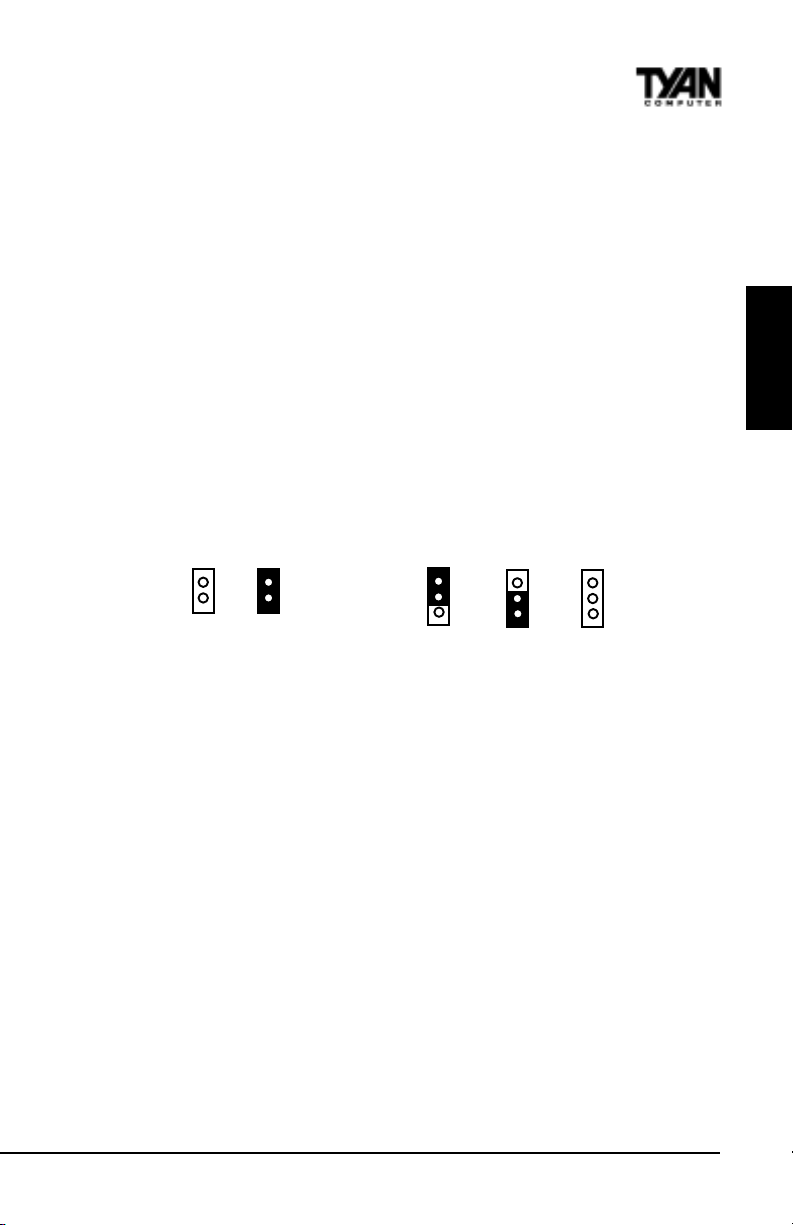
In this manual, the terms closed and on are used when referring to jumpers
(or jumper pins) that are active; open and off are used when referring to
jumpers (or jumper pins) that are inactive. See the Figure 2-1 for examples of
on and off pins and jumpers.
Jumpers and pins are connected by slipping the plastic jumper connector
overtop of two adjacent jumper pins (indicated by 1-2 or 2-3). The metal rod
inside the plastic shell bridges the gap between the two pins, completing the
circuit. See Figure 2-2 for more example of pin connections.
INSTALL
2 pin jumpers
off on
3 (or more) pin jumpers
1-2 2-3 open
1
2
3
1
2
3
1
2
3
Figure 2-1 Figure 2-2
The tables and maps on the following pages will help you set the jumpers for
CPU speed, infrared, and external connector pin assignments, among others. The
miniature motherboard maps will help you locate the jumpers on your board. A
full-page map of the motherboard can be found on the next two pages.
S2380 Trinity K7
11
Page 12

Chapter 2
Board Installation
Figure 2-3 : Map of Motherboard Jumpers
Mouse
Keyboard
USB0
USB1
Printer Port
COM2 COM1
Line out
Line inMicrophone in
Joystick
CD-IN
Video-IN
JP25
JP26
JP27
JP28
WOM1
WOL1
JP1
Slot A Type CPU
AGP port
PCI slot 1
PCI slot 2
PCI slot 3
PCI slot 4
PCI slot 5
PCI slot 6
ISA slot
ATX power connector
VIA
VT8371
JP22
JP19
FAN 1
FAN 3
1
JP20
1
DIMM bank 1
VIA
VT82C686A
JP24
1
1
1
DIMM bank 3
DIMM bank 2
Secondary IDE connector
JP18
3 volt
lithium
1
battery
1
FAN2
J2
1
Award BIOS
Floppy drive connector
Primary IDE connector
1
JP21
Clear CMOS
J1
1
The tiny 1s next to jumpers of 3 pins or more indicate the position of pin 1
for that jumper.
http://www.tyan.com
12
Page 13
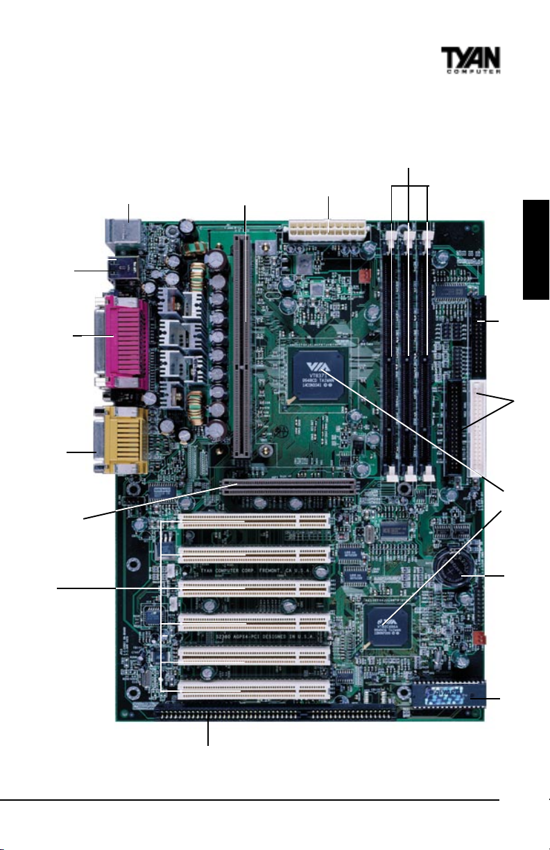
Figure 2-4 : Map of S2380 Features
PS/2 Mouse &
Keyboard
ports
2 USB ports
ports
1 Parallel, 2 Com
Joystick / Audio ports
4x AGP port
Slot A Type for
AMD Athlon K7
CPU
ATX power
3 DIMM slots
supply header
INSTALL
Floppy port
2-ch EIDE
Via KX-133 AGPset
Battery
6 PCI slots
S2380 Trinity K7
BIOS
1 ISA slot
13
Page 14
Chapter 2
Board Installation
1. Setting Jumpers
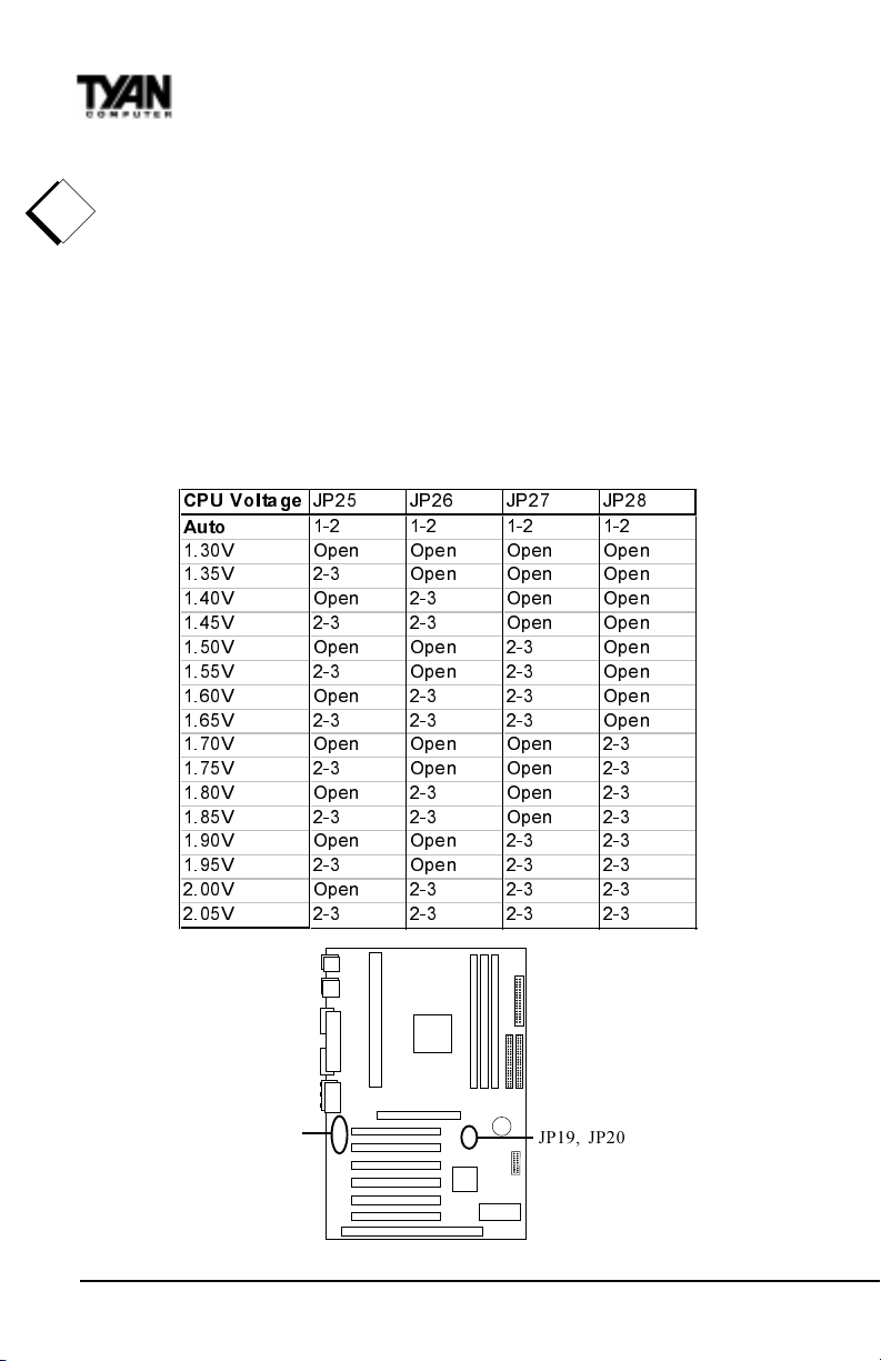
1-A. CPU Speed Settings (Auto-Detected)
!
The CPU speed settings are Auto-Detected by the CPU. The CPU voltage may
important!
be changed by using jumpers JP25-JP28. After the system is ready to boot, the
BUS Speed is auto-detected although you may set the BUS speed manually
using jumpers JP19 and JP20 . Presently all Athlon CPUs use a 200MHz bus
speed. (200 Mhz is at 100 Mhz DDR Double Data Rate).
Tyan does not recommend operating CPUs, memory, or PCI Bus at higher
than rated speed. Tyan takes no responsibility for any problems related to
overclocking any bus or component on the system board.
&389 ROWDJH
$XWR
9 2SHQ 2SHQ 2SHQ 2SHQ
9 2SHQ 2SHQ 2SHQ
9 2SHQ 2SHQ 2SHQ
9 2SHQ 2SHQ
9 2SHQ 2SHQ 2SHQ
9 2SHQ 2SHQ
9 2SHQ 2SHQ
9 2SHQ
9 2SHQ 2SHQ 2SHQ
9 2SHQ 2SHQ
9 2SHQ 2SHQ
9 2SHQ
9 2SHQ 2SHQ
9 2SHQ
9 2SHQ
9
JP25, JP26,
JP27, JP28
-3 -3 -3 -3
JP19, JP20
14
http://www.tyan.com
Page 15
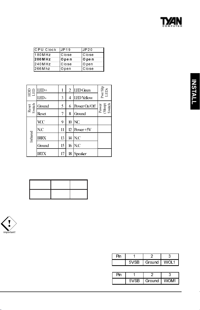
1-B CPU Clock Speed Settings (Jumper JP19 & JP20)
&38&ORFN -3 -3
0 +] &ORVH &ORVH
0+ ] 2SH Q 2SH Q
0 +] &ORVH 2SHQ
0 K] 2SHQ &ORVH
Default is Open / Open
1-C. Panel Connector Settings (Jumper J1)
'
'
/(' /('*UHHQ
'
(
/
+
/(' /('<HOORZ
K
W
F
H
*URXQG 3R ZHU2Q2II
W
V
L
H
Z
5
6
5HVH W * URX QG
9& & 1&
1 & 3RZHU9
G
H
U
D
U
,55; 1&
I
Q
,
S
O
V
6
'
U
(
Z
/
3
U
K
S
H
F
W
H
L
Z
H
O
R
Z
Power LED:
6
3
6
For 2-pin: bicolor/single
color - Use pins 2-4
For 3-pin: Use jumper JP22.
*URXQG 1&
,57; 6SHDNHU
1-F. Clear CMOS and Reset Password (Jumper JP21)
tluafeDteseR
12PJ
2-13-2
If you have been locked out of your system because you forgot your password
or set the CMOS incorrectly, follow the instructions below.
1. Power off the system, UNPLUG POWER CONNECTOR
!
important!
2. Set jumper JP21 to pins 2 and 3
3. Wait for 2 seconds, then return jumper JP21 to pins 1 and 2.
4. Power on the system again.
By following this procedure, you will erase your password and reset the CMOS
to the BIOS defaults.
3LQ
96% *URXQG :2/
1-D. Wake-On LAN (WOL1)
3LQ
1-E. Wake-On Modem (WOM1)
96% *URXQG : 20
INSTALL
S2380 Trinity K7
15
Page 16
Chapter 2
Board Installation
1-H Hardware Reset Switch Connector Installation
The Reset switch on your cases display panel provides you with the Hardware Reset function, which is the same as power on/off. The system will do a
cold start after the Reset button is pushed. (J1 pin 5 & 7)
1-I Onboard Sound audio Connectors (Video-In and CD-IN)
There are two 4-pin connectors onboard which are used for various peripherals audio signals. The digital signal that comes in through these connectors is
directed through the VIA KX-133 onboard sound function, and the digital
signal is turned into an audio signal which goes out through the speaker. This
consists of the VIDEO-IN connector for DVD drives and the CD-IN connector
is for CD-ROMs.
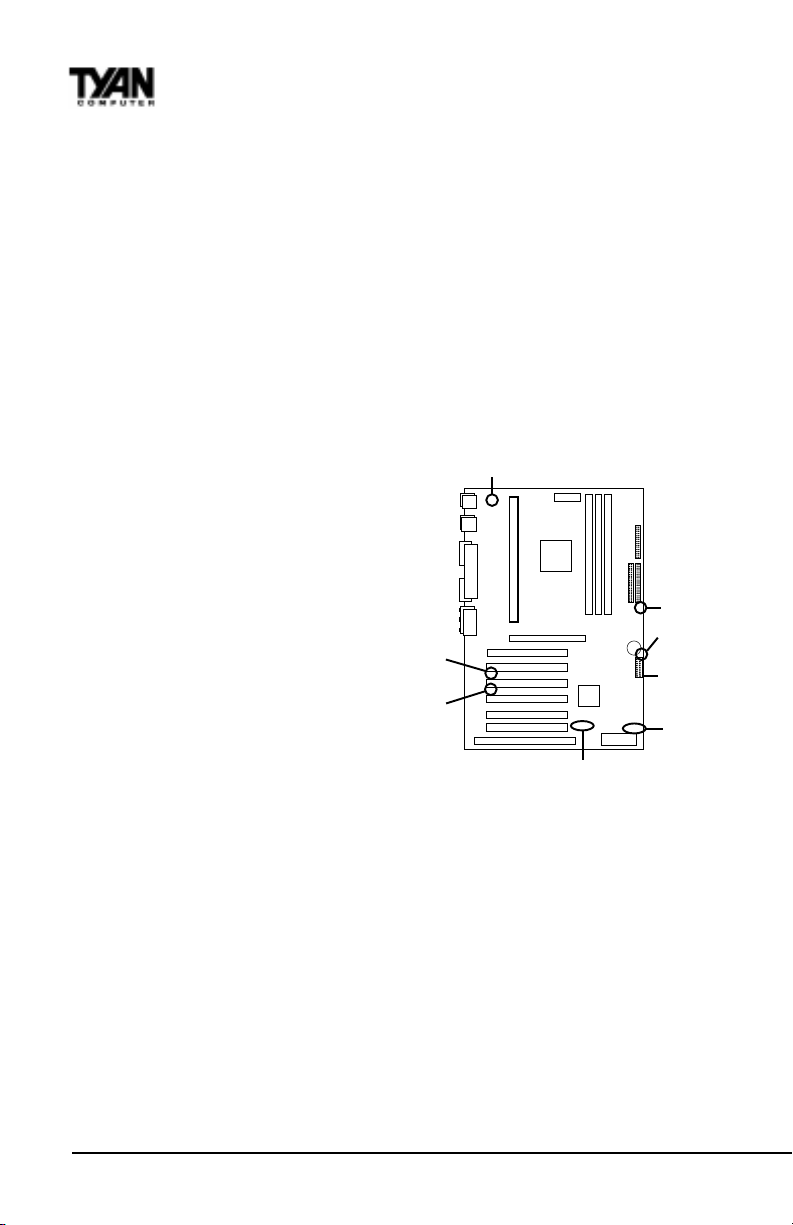
JP1
1-M. USB Header (Jumper
J2)
The Southbridge of the KX-133
chipset is capable of handling 4
USB ports. Only 2 connectors are
provided on the motherboard. If
you need to use all four ports, a
USB header (J2) is provided should
you decide to set up a USB
connector externally.
WOM
WOL
JP18
JP21
(Clr CMOS)
J1
J2 (USB)
JP22/ JP24
1-K Power LED Connector
(Jumper JP22)
Jumper JP22 is a three pin power LED header that can be used if you have a 3
pin Power LED. Otherwise refer to panel connector J16 for 2 pin LEDs. 3 pin
LEDs can still be used on J1 where pin 13 would be for the Ground pin.
Suspend to RAM ACPI Enable/Disable (Jumper JP18)
This jumper controls the ACPI advanced power management function . Set
the jumper JP18 to 1-2 to enable ACPI or set the jumper to 2-3 to turn the ACPI
function off. Default is OFF (2-3). ACPI must also be enabled in the BIOS in
order for this function to be activated. If ACPI is not enabled, the Sleep
Button (Jumper J24) will not function.
http://www.tyan.com
16
Page 17

External SMI (Jumper JP1)
The External SMI Signal Management Interupt header is reserved for use with
external hardware devices.
Sleep Button (Jumper JP24)
JP24 is used to connect to the sleep button. Depressing the sleep button will
send the computer into an S1 standby mode. During this mode the monitor
and harddisks are switched off. Hitting the keyboard or sleep button again will
wake up the computer.
CMOS RTC
The Real Time Clock (RTC) circuit, which provides the date and time for the
system is integrated into the Via KX-133 AGPset. If the external battery for the
RTC is low, it will prevent your system from POSTing, and you will not get a
display. Normally the life span of an external battery is 2 years. If yours is
running low, you will need to replace it with a new 3V lithium battery (Sony
CR2032).
Flash EEPROM
The Trinity K7 uses flash memory to store BIOS firmware. It can be updated as
new versions of the BIOS become available. You can upgrade your BIOS easily
using the flash utility (see page 61).
INSTALL
S2380 Trinity K7
17
Page 18

Chapter 2
Board Installation
2. Mounting the Motherboard in the Chassis
Follow the instructions provided by the case manufacturer for proper installation guidelines. TYAN recommends that you screw down the motherboard.
with all the mounting holes provided. If your case does not have a hole for a
standoff, simply cut off the bottom of the plastic standoff so that the flat
portion rests on the metal. The adapter cards and the screws holding them
down will keep your board flat. The fastening screw should not short any of
the traces on the motherboard. Make certain that you do not overtighten the
!
screw, as it will damage the motherboard and possibly break internal traces in
important!
the surrounding area. The hole you should use is located at the top-center of
the board where the adapter cards are fastened to the case.
3. Installing Memory
Since TYAN boards are manufactured with performance in mind, you should
use add-in components that match. It is highly recommended that the memory
DIMMs are installed prior to connecting the power supply. Some DIMM
modules may seem to be high quality because of name or feel but that does not
guarantee real-world usability. Some cheaper or OEM memory may have brandname components, but they may contain inferior or substandard parts which
do not meet the critical tolerances our products require. Because of this, your
memory may not work correctly in a TYAN board though it may work well in a
competitors board. This is because many of our competitors do not adhere to
the strict tolerances required for high performance. If you buy a TYAN board,
you are getting the best system available. To make installation easy and
trouble free, get high quality parts. Some brands we recommend are Advantage
Memory, Corsair Microsystems, Millenium, Kingston Memory, QesTec
Incorporated, Unigen, Micron Technology, and Crucial Technology. These
DIMMs have proven to be very stable on our boards and perform extremely
well.
warning
This motherboard operates on a 3.3 volt standby for the DIMM banks .
Because of this, you need to UNPLUG the AC power cord before installing
your DIMM memory modules. Otherwise, the motherboard may automatically
power up when the memory is inserted into the slot.
18
http://www.tyan.com
Page 19
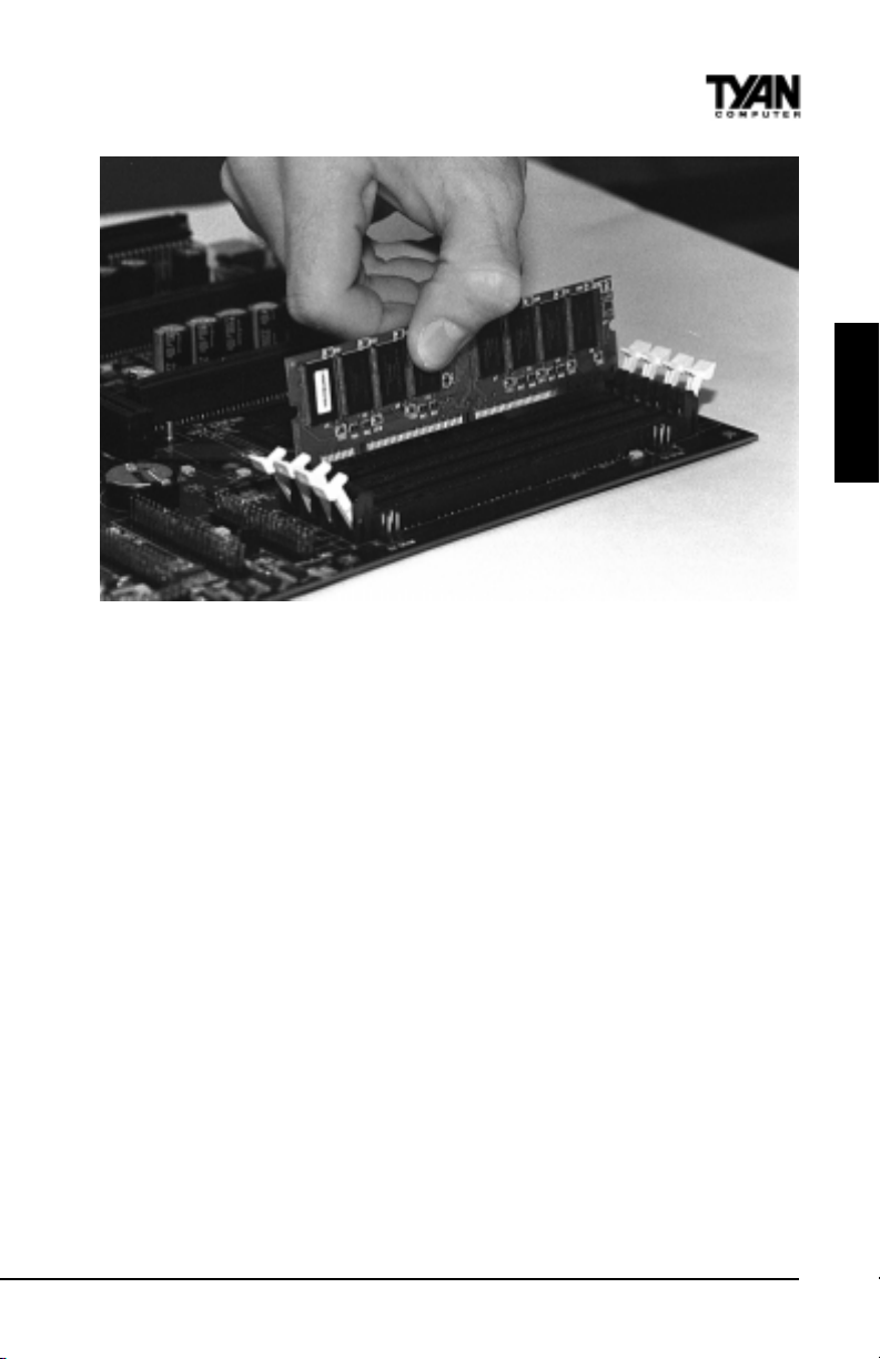
Figure 2-5*
*Note: The image above is used to illustrate a concept and may not represent the actual
image of your motherboard.
To install your DIMMs, line your module up so that the pins fit into the slot.
There is only one way that your DIMM can fit properly. Make sure that the
short row of pins is lined up with the short gap in the DIMM slot. Figure 2-5
shows how to sit the DIMM into its slot. To insert the DIMM, push down
vertically on the module with even force, as shown in the photo. Do not shove
one end in first; doing so will bend the DIMM pins.
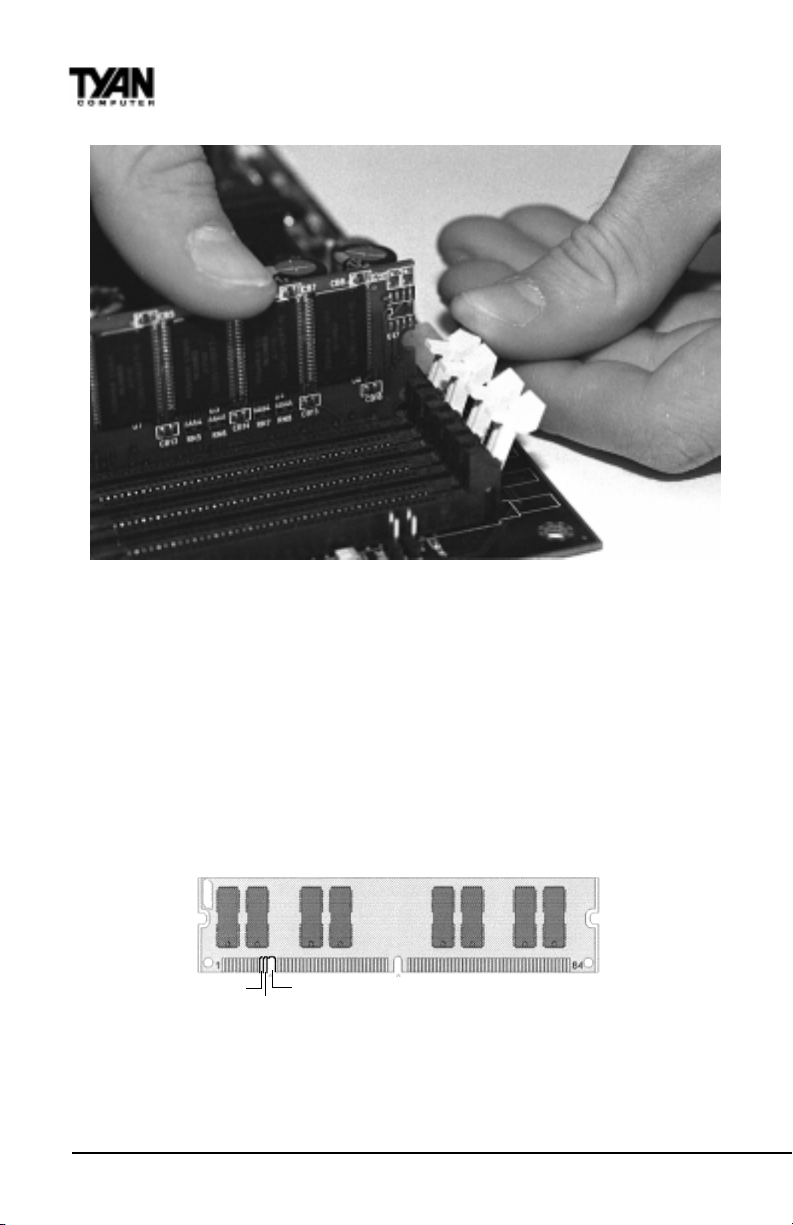
To lock the DIMM into place, push the plastic clips on either end of the slot
onto the notches in the ends of the DIMM (see Figure 2-6 on the next page).
To remove your DIMM, simply pull the clips back, and pull up on the module.
INSTALL
Place the DIMMs in an anti-static bag as soon as you remove them to avoid
static damage.
S2380 Trinity K7
19
Page 20
Chapter 2
Board Installation
Figure 2-6*
*Note: The image above is used to illustrate a concept and may not represent the actual
image of your motherboard.
The Trinity K7 uses a 64-bit data path from memory to CPU and can accommodate up to 1 GB of SDRAM. The 168-pin DIMMs (Dual In-line Memory
Modules) must be of the 3.3V, unbuffered variety. The position of the notch in
the SDRAM key position will tell you whether or not a DIMM is unbuffered
(see the Figure 2-7 below). All installed memory will be automatically detected,
so there is no need to set any jumpers.
Buffered
Unbuffered
168-pin DIMM
RFU
Figure 2-7
http://www.tyan.com
20
Page 21

Some details of memory installation:
At least one unbuffered DIMM must be installed for the system to POST.
The mainboard supports 32MB, 64MB, 128MB, 256MB and 512MB
SDRAM.
Memory supports for PC100, PC133 and VCM Memory.
Registered DIMMs are not supported on this motherboard
The table below shows some of the possible memory configurations. Not all
possible configurations are listed.
1knaBMMID2knaBMMID3knaBMMIDlatoT
1xBM800BM8
1xBM81xBM80BM61
1xBM81xBM81xBM8BM42
1xBM611xBM81xBM8BM23
1xBM611xBM611xBM8BM04
1xBM611xBM611xBM61BM84
1xBM231xBM611xBM61BM46
1xBM231xBM231xBM61BM08
1xBM231xBM231xBM23BM69
1xBM461xBM231xBM23BM821
1xBM461xBM461xBM23BM061
1xBM461xBM461xBM46BM291
1xBM8211xBM461xBM46BM652
1xBM8211xBM8211xBM46BM023
1xBM8211xBM8211xBM821BM483
1xBM6521xBM6520BM215
1xBM6521xBM6521xBM652BM867
1xBM2151xBM2151xBM215*BG5.1
INSTALL
*1.5GB memory onboard not verified at time of print please see website for details.
S2380 Trinity K7
21
Page 22
Chapter 2
Board Installation
Installing the SlotA CPU and Cooling Fan
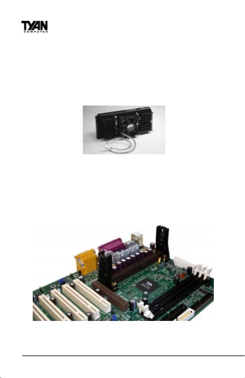
Using a cooling mechanism for Athlon K7 processors is extremely important. The
active cooler shown in Figure 2-8 below is equipped with a cooling fan and heat
sink, allowing better air flow and heat dissipation for the CPU. The size of the
cooling mechanism will not interfere with CPU installation. The CPU will fit with
ease into the CPU slot of the Trinity K7 board.
Figure 2-8
Figure 2-9 below shows an overhead view of the retention braces positioned at
both ends of the CPU slot. Be sure to tighten the retention brace screws to
secure them onto the motherboard.
Figure 2-9
http://www.tyan.com
22
Page 23
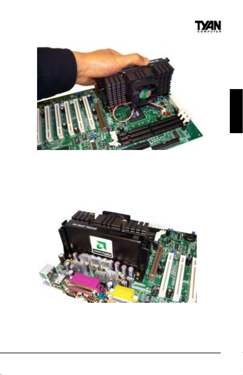
Figure 2-10
Carefully line up the pins of the CPU with the pins of the Slot while placing the
CPU between the two retention braces (the CPU cooling fan should face the
memory DIMM sockets). Lower the CPU onto the motherboard (see Figure 210 above). Your CPU will be firmly secured onto the motherboard once the
retention braces snap into the sides of the CPU. The installed CPU should
look like Figure 2-11 below.
Figure 2-11
INSTALL
You will also need to connect the CPUs cooling fan cable to the cooling fan
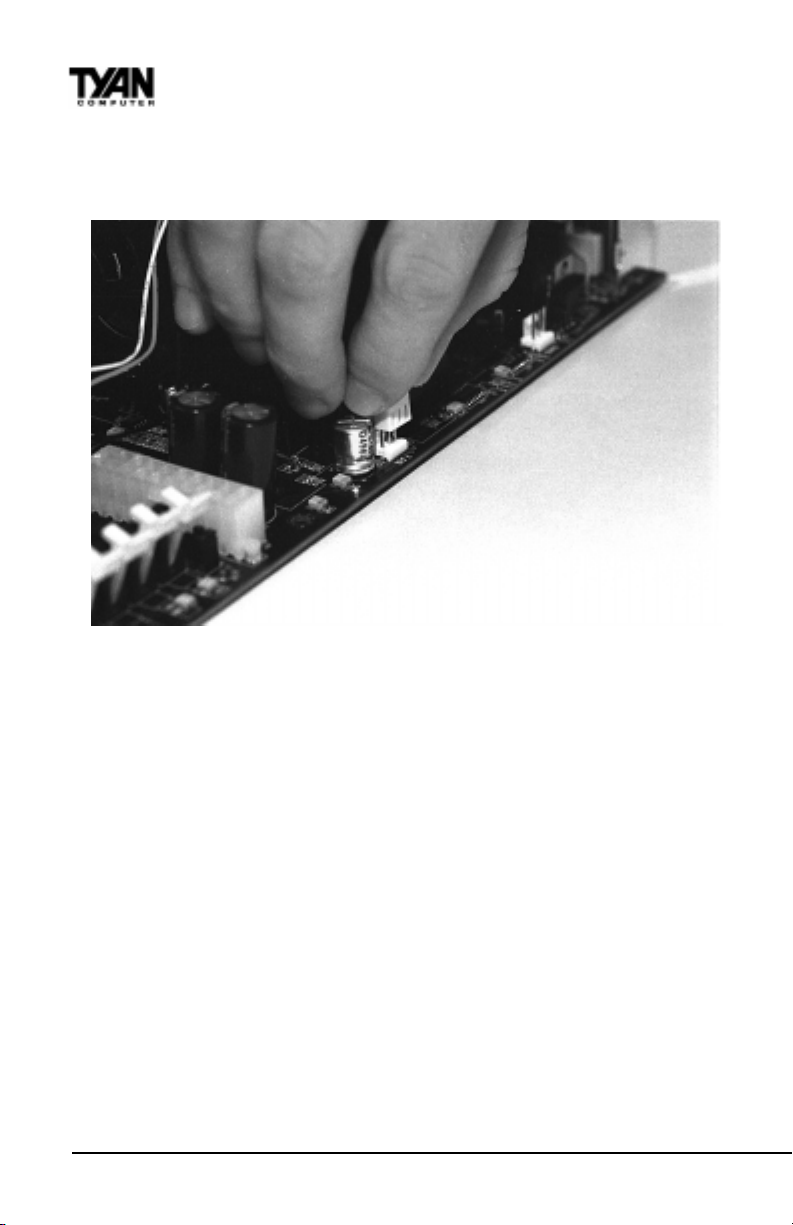
power connector on the board. Locate the cooling fan connector (e.g. FAN1)
on the motherboard. Plug the CPUs cooling fan cable into the cooling fan
S2380 Trinity K7
23
Page 24
Chapter 2
Board Installation
connector on the board. There will be a plastic clip assembly similar to that of
the ATX power connector that will force you to connect the fan cable correctly
see Figure 2-12 below.
Figure 2-12
Removing CPU
To remove the CPU, gently bend the sides of the retention brace away from the
CPU and slowly pull the CPU upwards. This may require careful firm tugs to
pull the CPU out of its slot.
5. Connecting IDE and Floppy Drives
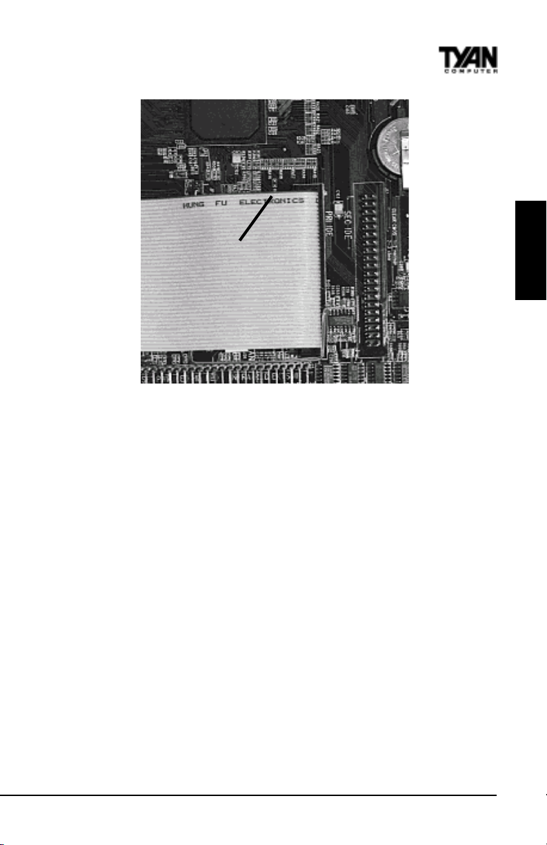
The colored stripe on a ribbon cable should be plugged into Pin 1. The primary
IDE connector is black; the secondary IDE connector is white. In most cases,
this is the proper way of connecting your IDE cable to the hard drive. Figure
2-13 on the following page shows the IDE cable properly connected to the
motherboard. Contact your hard disk drive manufacturer or documentation for
more information.
Some symptoms of incorrectly installed HDDs are:
Hard disk drives are not auto-detected: may be a Master/Slave
problem or a bad IDE cable. Contact your vendor.
Hard Disk Drive Fail message at bootup: may be a bad cable or
lack of power going to the drive.
http://www.tyan.com
24
Page 25
Pin 1
INSTALL
*Note: The image above is used to illustrate a concept and may not represent the actual
image of your motherboard.
No video or beeps onbootup: usually means the cable is on back
Figure 2-13*
wards.
Hard drive lights are constantly on: bad IDE cable or defective drives/
motherboard. Try another HDD.
Hard drives do not power up: check power cables and cabling.
May also be a bad power supply or IDE drive.
Connecting Floppy Drives
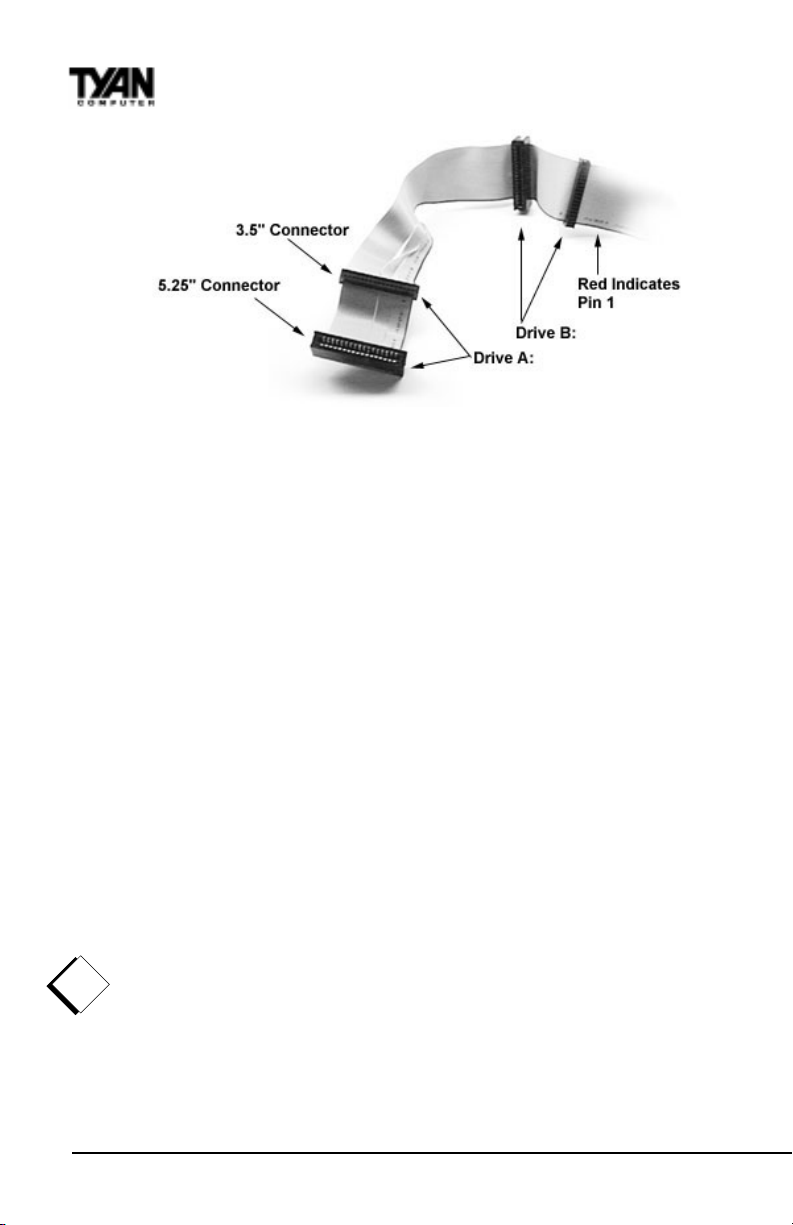
Pin 1 on the floppy cable is usually denoted by a red or colored stripe down
one side of the cable (see Figure 2-14 on the following page). Most of the
current floppy drives on the market require that the colored stripe be positioned so that it is right next to the power connector. In most cases, there will
be a key pin on the cable which will force you to connect the cable properly.
Drive A: is usually attached to the end of the cable with the twist in it. Drive B:
is usually connected to the middle of the cable. Refer to your installation
instructions or call your dealer if you are unsure about attaching floppy drives.
Refer to Figure 2-14 on the following page for a detailed anatomy of the floppy
cable. Remember, you can only have 2 floppy drives connected at any given
time.
S2380 Trinity K7
25
Page 26
Chapter 2
Board Installation
Figure 2-14
The color stripe on the cable should face toward the top of your chassis, or
toward the battery on the motherboard. Please refer to your documentation for
proper installation.
Some symptoms of incorrectly installed floppies are:
Floppy drives are not detected: usually caused by faulty cables,
backward cables, or a bad floppy or motherboard. Try another single
floppy drive to verify the problem or try another cable. Also, check to
see if the onboard floppy is enabled in the BIOS.
Floppy Drive Fail message at bootup: the cable, floppy, or
motherboard may be faulty. Try another cable or floppy drive to
verify.
Light on the floppy is on constantly: a definite giveaway that the
cable is on backwards. Reverse the cable at the motherboard end and
try again.
6. Installing Add-on Cards
There are a few rules you need to follow when plugging in a card. In order to
assure proper operation and a quick installation, adhere to these guidelines:
NEVER force a card into a slot. If it doesnt fit, look at the
!
important!
socket on the computer to make sure there are no wires or
other obstructions to the slot.
NEVER plug an ISA card into a PCI slot or a PCI card in an ISA
slot. You will void your warranty and damage your system board if
you do this.
http://www.tyan.com
26
Page 27

When plugging the card in, especially when installing long cards,
try to push the entire card in at one time. Dont force one end of
the card into the socket first and then the other. This will create a
rocking motion between the card and the slot and it will damage the
pins within the socket.
Make sure that the cards are seated securely into the slots.
Before turning on the system, make sure no cards are touching
warning
NOTE: This motherboard operates on a 3.3 volt standby for PCI
v2.2. Because of this, you need to UNPLUG the AC power cord
before installing your card. Otherwise, the motherboard may
automatically power up when the card is inserted into the slot.
If you follow these basic guidelines, there shouldnt be any problems with
installation. However, if you do encounter any problems, have a qualified
professional install your cards for you or contact your card manufacturer.
Remember, always read the manuals and installation notes that come with the
adapter cards. They contain important information which will help you install
the components right, the first time.
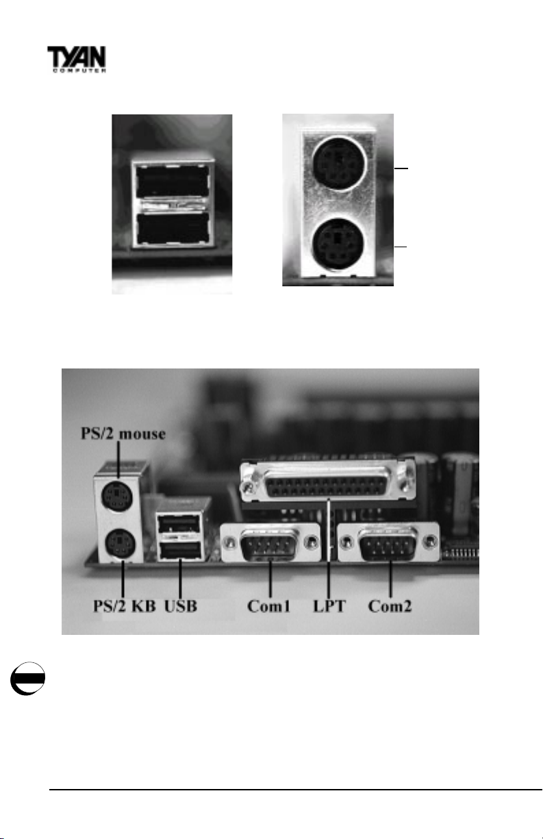
7. Connecting PS/2, USB, Serial & Parallel Devices
This board includes ports for USB, PS/2 mouse, and PS/2 keyboard devices.
Note that, for this board, the PS/2 mouse port is the upper PS/2 port, and the
PS/2 keyboard port is the lower PS/2 port. The PS/2 connectors are probably
quite familiar to you. The USB connectors, however, may be foreign. The USB
(Universal Serial Bus) is a versatile port. This one port type can function as a
serial, parallel, mouse, keyboard, or joystick port. It is fast enough to support
video transfer, and is capable of supporting up to 127 daisy-chained peripheral
devices. Figures 2-15 and 2-16 on the following page shows the USB ports on
the left and PS/2 ports on the right (respectively).
INSTALL
S2380 Trinity K7
27
Page 28
Chapter 2
Board Installation
Figure 2-15 Figure 2-16
Connecting Com and Printer Ports
Mouse
Keyboard
Figure 2-17
Warning: When plugging in your keyboard and mouse, or when plugging
warning
anything into a serial or Com port, make sure that the power is off. Connecting
these devices and ports while the power is on is called hot plugging, and may
damage your system. Figure 2-17 above shows the ATX double row connectors
on this board. The Com and Printer ports, as well as the other ports, are labeled.
28
http://www.tyan.com
Page 29
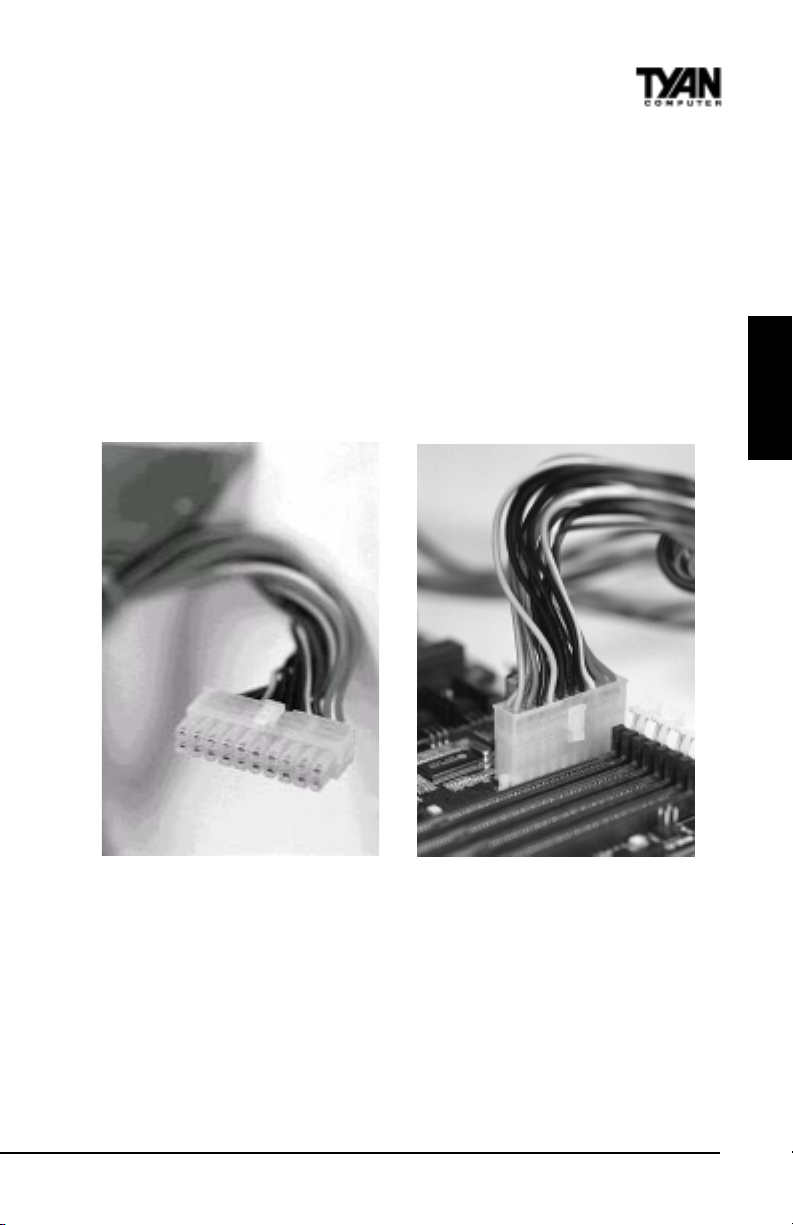
8. Connecting the Power Supply
Tyan recommends using an ATX power supply that conforms to industry
standard revision 2.01. The Trinity K7 motherboard comes equipped with one
onboard power connector. Figure 2-18 shows an ATX power connector.
When plugging in the power connector, make sure that the plastic clip on the
power connector is aligned with the plastic tab on the onboard connector (See
Figure 2-19 below) . Make certain that you do not miss any pins because if
you do, you will void your warranty and cause damage to yourself or your
motherboard when you turn the system on. After connecting the power, make
sure the connector is seated firmly into its socket so it will not become loose or
fall off when the computer is jostled or moved.
INSTALL
ONBOARD
Figure 2-18
You are done!
Other than checking the jumper settings and cable connections and putting
the case back on, you are done. Installing a new motherboard may sound
difficult, but by following these directions, you should have a fairly uneventful
time installing our products. If you do encounter problems, your dealer will be
able to help you, or you can consult one of our many technical support
resources (see page 8).
S2380 Trinity K7
29
Figure 2-19
Page 30
Chapter 3
BIOS Configuration
chapter 3
BIOS Configuration
Introduction to Setup
The BIOS section of the manual is subjected to change without notice and is
!
provided here for reference purposes only. The settings and configurations
important!
of the BIOS are current at the time of print, although they may not be exactly
the same as that displayed on your screen.
This manual describes the Award BIOS Setup program. The Setup program lets
you modify basic system configuration settings. The settings are then stored
in a dedicated battery-backed memory, called NVRAM, that retains the
information when the power is turned off.
The Award BIOS in your computer is a customized version of an industrystandard BIOS for IBM PC ATcompatible personal computers. It supports
AMD Athlon K7 and compatible processors. The BIOS provides critical lowlevel support for the system central processing, memory, and I/O subsystems.
The Award BIOS has been customized by adding important, but nonstandard,
features such as virus and password protection, power management, and
detailed fine-tuning of the chipset controlling the system. The rest of this
manual is intended to guide you through the process of configuring your
system using Setup.
http://www.tyan.com
30
Page 31

Starting Setup
The Award BIOS is immediately activated when you first turn on the computer.
The BIOS reads system configuration information in CMOS RAM and begins
the process of checking out the system and configuring it through the poweron self test (POST).
When these preliminaries are finished, the BIOS seeks an operating system on
one of the data storage devices (hard drive, floppy drive, etc.). The BIOS
launches the operating system and hands control of system operations to it.
During POST, you can start the Setup program in one of two ways:
1. By pressing <Del> immediately after switching the system on, or
2. By pressing the <Del> key when the following message appears briefly at
the bottom of the screen during POST:
TO ENTER SETUP BEFORE BOOT PRESS DEL KEY
If the message disappears before you respond and you still wish to enter
Setup, restart the system to try again by turning it OFF then ON or pressing
the RESET button on the system case. You may also restart by simultaneously
pressing <Ctrl>, <Alt>, and <Delete> keys. If you do not press the keys at the
correct time and the system does not boot, an error message appears and you
are again asked to
PRESS F1 TO CONTINUE, DEL TO ENTER SETUP
Setup Keys
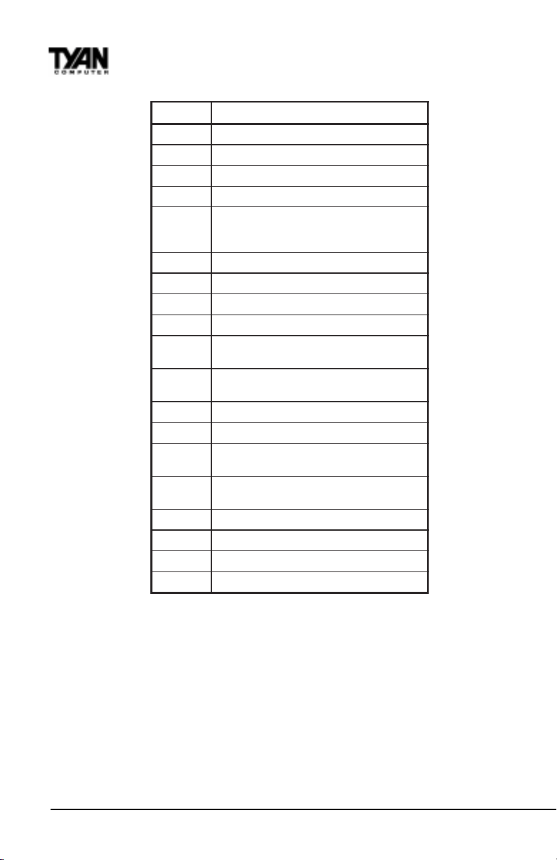
The table on the following page shows how to navigate in Setup using the
keyboard.
Getting Help
Press F1 to pop up a small help window that describes the appropriate keys to
use and the possible selections for the highlighted item. To exit the Help
Window press <Esc> or the F1 key again.
BIOS
S2380 Trinity K7
31
Page 32
Chapter 3
BIOS Configuration
yeKnoitcnuF
worrapU.metisuoiverpotevoM
worranwoD.metitxenotevoM
worratfeL.dnahtfelehtnonetiotevoM
worrathgiR.dnahthgirehtnometiotevoM
yekcsE
yekpUgP.segnahcekamroeulavciremunehtesaercnI
yeknDgP.segnahcekamroeulavciremunehtesaerceD
yek+.segnahcekamroeulavciremunehtesaercnI
yek-.segnahcekamroeulavciremunehtesaerceD
yek1F
yek2F
2F-tfihS
yek3F.uneMputeSegaPsutatSrofylno,radnelaC
yek4F.devreseR
yek5F
yek6F
yek7F.tluafedehtdaoL
yek8F.devreseR
yek9F.devreseR
yek01F.uneMniaMrofylno,segnahcSOMCehtllaevaS
otnisegnahcevastonoddnatiuQ:uneMniaM
tixE:uneMputeSegaPsutatS.MARSOMC
.uneMniaMotnruterdnaegaptnerruc
dnauneMputeSegaPsutatSrofylno,plehlareneG
.uneMputeSegaPnoitpO
tcelesot2F.sroloc61latotmorfrolocegnahC
.sdrawkcabroloctcelesot2F-tfihS,drawrofroloc
,SOMCmorfeulavSOMCsuoiverpehterotseR
.uneMputeSegaPnoitpOrofylno
SOIBmorfeulavMARSOMCtluafedehtdaoL
.uneMputeSegaPnoitpOrofylno,elbattluafed
In Case of Problems
If, after making and saving system changes with Setup, you discover that your
computer is no longer able to boot, restart by either using the ON/OFF
switch, the RESET button or by pressing <Ctrl>, <Alt> and <Delete> at the
same time, or clear the CMOS (see page 15 for details) The best advice is to
alter only settings that you thoroughly understand. In particular, do not
change settings in the Chipset screen without a good reason. The Chipset
defaults have been carefully chosen by Award Software or your system
manufacturer for the best performance and reliability. Even a seemingly small
change to the Chipset setup may causing the system to become unstable.
http://www.tyan.com
32
Page 33
Setup Variations
Not all systems have the same Setup. While the basic look and function of the
Setup program remains the same for all systems, the appearance of your Setup
screens may differ from the screens shown here. Each system design and
chipset combination require custom configurations. In addition, the final
appearance of the Setup program depends on your system designer. Your
system designer can decide that certain items should not be available for user
configuration and remove them from the Setup program.
Main Setup Menu
When you enter the AwardBIOS CMOS Setup Utility, a Main Menu, similar to
the one shown below, appears on the screen. The Main Menu allows you to
select from several Setup functions and two exit choices. Use the arrow keys to
select among the items and press enter to accept and enter the sub-menu.
A brief description of each highlighted selection appears at the bottom of the
screen. Following is a brief summary of each Setup category.
CMOS Setup Utility - Copyright (C) 1984-2000 Award Software
w
Standard CMOS Features Load Fail-Safe Defaults
w
Advanced BIOS Features Load Optimized Defaults
w
Advanced Chipset Features Set Supervisor Password
w
Integrated Peripherals Set User Password
w
Power Management Setup Save & Exit Setup
w
PnP/PCI Configurations Exit Without Saving
w
PC Health Status
BIOS
Esc : Quit ↑ ↓ → ← : Select Item
F10 : Save & Exit Setup (Shift)F2 : Change Color
S2380 Trinity K7
33
Page 34

Chapter 3
BIOS Configuration
Standard CMOS Features
Options in the original PC AT-compatible BIOS.
Advanced BIOS Features
Award Software enhanced BIOS options.
Advanced Chipset Features
Options specific to your system chipset.
Integrated Peripherals
I/O subsystems that depend on the integrated peripherals controller in your
system.
Power Management Setup
Advanced Power Management (APM) options.
PnP/PCI Configurations
Plug and Play standard and PCI Local Bus configuration options.
PC Health Status
Displays CPU / System Temperature and Fan Speeds
Load Fail-Safe Defaults
BIOS defaults are factory settings for the most stable, minimal-performance
system operations.
Load Optimized Defaults
Setup defaults are factory settings for optimal-performance system operations.
Set Supervisor Password
Change, set, or disable a password. Only the supervisor password permits
access to Setup.
Set User Password
Change, set, or disable a password. The user password generally allows only
power-on access.
Save & Exit Setup
Save settings in nonvolatile CMOS RAM and exit Setup.
Exit Without Saving
Abandon all changes and exit Setup.
http://www.tyan.com
34
Page 35
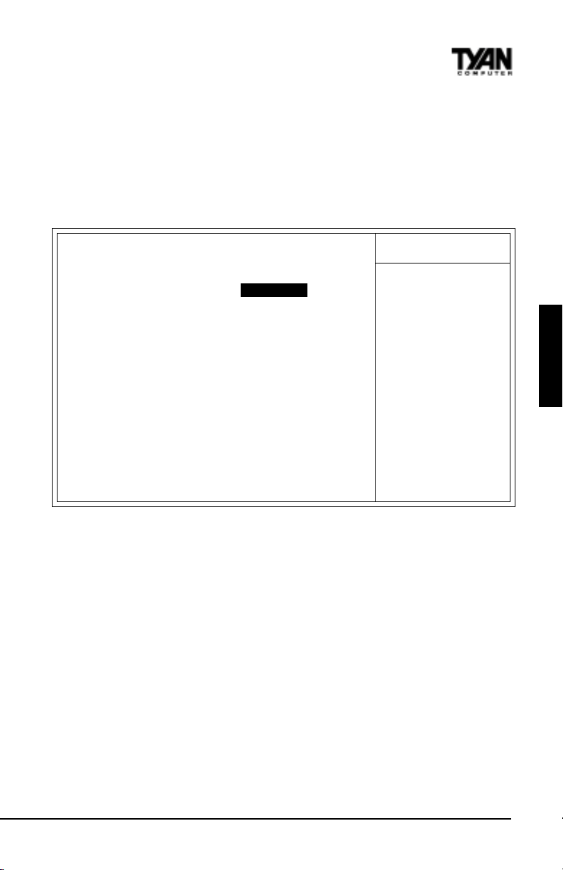
Standard CMOS Features
In the Standard CMOS menu you can set the system clock and calendar, record
disk drive parameters and the video subsystem type, and select the type of
errors that stop the BIOS POST.
CMOS Setup Utility - Copyright (C) 1984-2000 Award Software
Standard CMOS Features
Date (mm:dd:yy) Sat, Jan 1 2000 Item Help
Time (hh:mm:ss) 0 : 10: 30
w
IDE Primary Master Press Enter None
w
IDE Primary Slave Press Enter None To enter next page for
w
IDE Secondary Master Press Enter None detail hard drive
w
IDE Secondary Slave Press Enter None settings
Drive A 1.44M, 3.5 in.
Drive B None
Video EGA/VGA
Halt On All,But Keyboard
Base Memory 640K
Extended Memory 31744K
Total Memory 32768K
↑ ↓ → ← :Move Enter:Select +/-/PU/PD:Value F10:Save ESC:Exit F1:General Help
F5:Previous Values F6:Fail-Safe Defaults F7:Optimized Defaults
Menu Level
w
BIOS
Date
The BIOS determines the day of the week from the other date information. This
field is for information only. Press the arrow keys to move to the desired field
(date, month, year). Press the PgUp or PgDn key to increment the setting, or
type the desired value into the field.
Time
The time format is based on the 24-hour military-time clock. For example, 1 p.m.
is 13:00:00. Press the arrow keys to move to the desired field. Press the PgUp or
PgDn key to increment the setting, or type the desired value into the field.
S2380 Trinity K7
35
Page 36

Chapter 3
BIOS Configuration
IDE Primary/Secondary, Master/Slave
CMOS Setup Utility - Copyright (C) 1984-2000 Award Software
IDE Primary Master
IDE HDD Auto-Detection Press Enter Item Help
w
IDE Primary Master Auto Menu Level
Access Mode Auto
To auto-detect the
Capacity 0 MB HDDs size, head... on
this channel
Cylinder 0
Head 0
Precomp 0
Landing Zone 0
Sector 0
↑ ↓ → ← :Move Enter:Select +/-/PU/PD:Value F10:Save ESC:Exit F1:General Help
F5:Previous Values F6:Fail-Safe Defaults F7:Optimized Defaults
w
The BIOS supports up to four IDE drives (IDE Primary/Secondary Master/
Slave). This section does not show information about other IDE devices, such
as a CD-ROM drive, or about other hard drive types, such as SCSI drives.
Note: We recommend that you select type auto for all drives.
The BIOS can automatically detect the specifications and optimal operating
mode of almost all IDE hard drives. When you select auto for the hard drive
option (IDE Primary/Secondary Master/Slave), the BIOS detects its specifications during POST, every time the system boots. If you do not want to select
auto, other methods of selecting the drive type are available:
1. Match the specifications of your installed IDE hard drive(s) with the
preprogrammed values for drive types 1 through 45.
2. Select Manual and enter values into each drive parameter field.
3. Use the IDE HDD Auto Dectection function in Setup .
http://www.tyan.com
36
Page 37

The following is a brief explanation of drive specifications:
Type:
The BIOS contains a table of pre-defined drive types. Each defined drive type
has a specified number of cylinders, number of heads, write precompensation
factor, landing zone, and number of sectors. Drives whose specifications do
not accommodate any pre-defined type are classified as type user.
Size:
Disk drive capacity (approximate). Note that this size is usually slightly greater
than the size of a formatted disk given by a disk-checking program.
Cyls: Number of cylinders
Head: Number of heads
Precomp: Write precompensation cylinder
Landz: Landing zone
Sector: Number of sectors
Access Mode: Auto, Normal, large, or LBA
Auto: The BIOS automatically determines the optimal mode.
Normal: Maximum number of cylinders, heads, and sectors
supported are 1024, 16, and 63.
Large: For drives that do not support LBA and have more than 1024
cylinders.
LBA (Logical Block Addressing): During drive accesses, the IDE
controller transforms the data address described by sector, head, and
cylinder number into a physical block address, significantly
improving data transfer rates. For drives with greater than 1024
cylinders.
BIOS
S2380 Trinity K7
37
Page 38

Chapter 3
BIOS Configuration
Drive A
Select the correct specifications for the diskette drive(s) installed in the
computer.
enoNdellatsnievirdetteksidoN
ni52.5,K063yticapacetybolik063;evirddradnatsepyt-CPhcni4/1-5
ni52.5,M2.1yticapacetybagem2.1;evirdytisned-hgihepyt-TAhcni4/1-5
ni5.3,K027yticapacetybolik027;evirddedis-elbuodhcni2/1-3
ni5.3,M44.1yticapacetybagem44.1;evirddedis-elbuodhcni2/1-3
ni5.3,M88.2yticapacetybagem88.2;evirddedis-elbuodhcni2/1-3
Video
Select the type of primary video subsystem in your computer. The BIOS
usually detects the correct video type automatically. The BIOS supports a
secondary video subsystem, but you do not select it in Setup.
AGV/AGE
04AGC.edomnmuloc04nipurewop,retpadAscihparGroloC
08AGC.edomnmuloc08nipurewop,retpadAscihparGroloC
.sretpadarotinomAGPro,AGVS,AGES
,AGV,AGEroF.yarrAscihparGoediV/retpadAscihparGdecnahnE
ONOM .sretpadaemorhconomnoituloserhgihsedulcni,retapdaemorhconoM
Halt On
During the power-on self-test (POST), the computer stops if the BIOS detects
a hardware error. You can tell the BIOS to ignore certain errors during POST
and continue the boot-up process. These are the selections:
srorreoN.srorreynarofpotstonseodTSOP
srorrellA
draobyeKtuB,llA .srorrerehtollarofspotstub,rorredraobyekarofpotstonseodTSOP
etteksiDtuB,llA
yeK/ksiDtuB,llA
.srorre
.srorre
.noitcaevitcerrocekat
38
otuoystpmorpdnaspotsTSOP,rorrelataf-nonynastcetedSOIBehtfI
rehtollarofspotstub,srorreevirdetteksidrofpotstonseodTSOP
rehtollarofspotstub,rorreksidrodraobyekarofpotstonseodTSOP
http://www.tyan.com
Page 39

Memory
You cannot change any values in the Memory fields; they are only for your
information. The fields show the total installed random access memory (RAM)
and amounts allocated to base memory, extended memory, and other (high)
memory. RAM is counted in kilobytes (KB: approximately one thousand bytes)
and megabytes (MB: approximately one million bytes).
RAM is the computers working memory, where the computer stores programs
and data currently being used, so they are accessible to the CPU. Modern
personal computers may contain up to 64 MB, 128 MB, or more.
Base Memory: Typically 640 KB. Also called conventional memory.
The DOS operating system and conventional applications use this
area.
Extended Memory: Above the 1-MB boundary. Early IBM personal
computers could not use memory above 1 MB, but current PCs and
their software can use extended memory.
Total Memory: Displays the total memory in the system.
BIOS
S2380 Trinity K7
39
Page 40
Chapter 3
BIOS Configuration
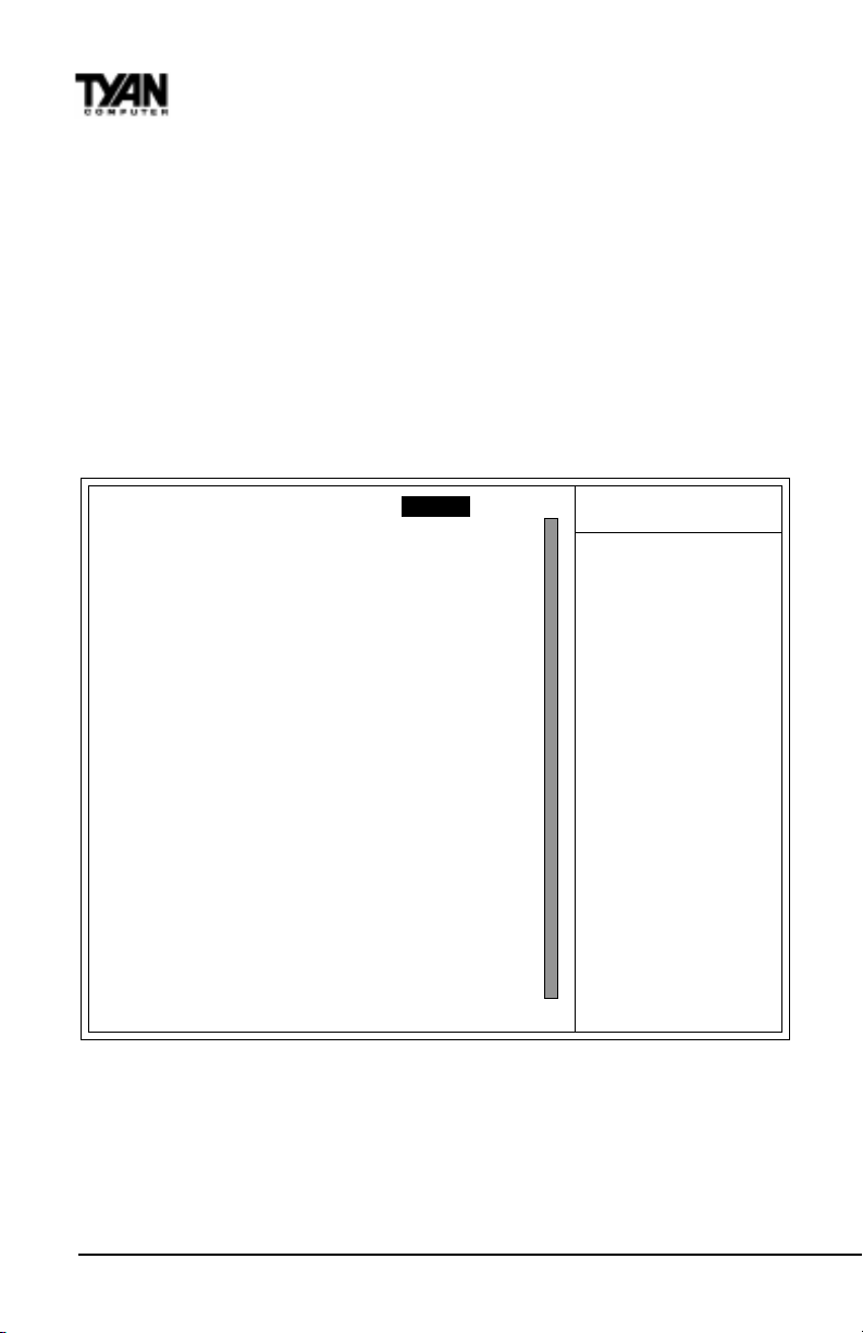
Advanced BIOS Features
The screen (shown on the following page) contains industry-standard options
additional to the core PC AT BIOS. This section describes all fields offered by
Award Software in this screen. The example screen below may vary from the
one in your Setup program. Your system board designer may omit or modify
some fields.
Advanced BIOS Features - Fail-Safe Defaults
CMOS Setup Utility - Copyright (C) 1984-2000 Award Software
Standard CMOS Features
Virus Warning Enabled Item Help
CPU Internal Cache Enabled
External Cache Enabled Menu Level
CPU L2 Cache ECC Checking Enabled
Quick Power On Self Test Enabled Allows you to choose
First Boot Device Floppy the VIRUS warning
Second Boot Device HDD-0 feature for IDE Hard
Third Boot Device LS120 Disk boot sector
Boot Other Device Enabled protection. If this
Swap Floppy Drive Disabled function is enabled
Boot Up Floppy Seek Enabled and someone attempts
Boot Up NumLock Status On to write data into this
Gate A20 Option Normal area, BIOS will show a
Typematic Rate Setting Disabled warning message on
X Typematic Rate (Chars/Sec) 6 screen and alarm beep
X Typematic Delay (Msec) 250
Security Option Setup
OS Select For DRAM > 64MB Non-OS2
Video BIOS Shadow Enabled
C8000-CBFFF Shadow Disabled
CC000-CFFFF Shadow Disabled
D0000-D3FFF Shadow Disabled
D4000-D7FFF Shadow Disabled
D8000-DBFFF Shadow Disabled
DC000-CFFFF Shadow Disabled
↑ ↓ → ← :Move Enter:Select +/-/PU/PD:Value F10:Save ESC:Exit F1:General Help
F5:Previous Values F6:Fail-Safe Defaults F7:Optimized Defaults
▲
w
▲
40
http://www.tyan.com
Page 41
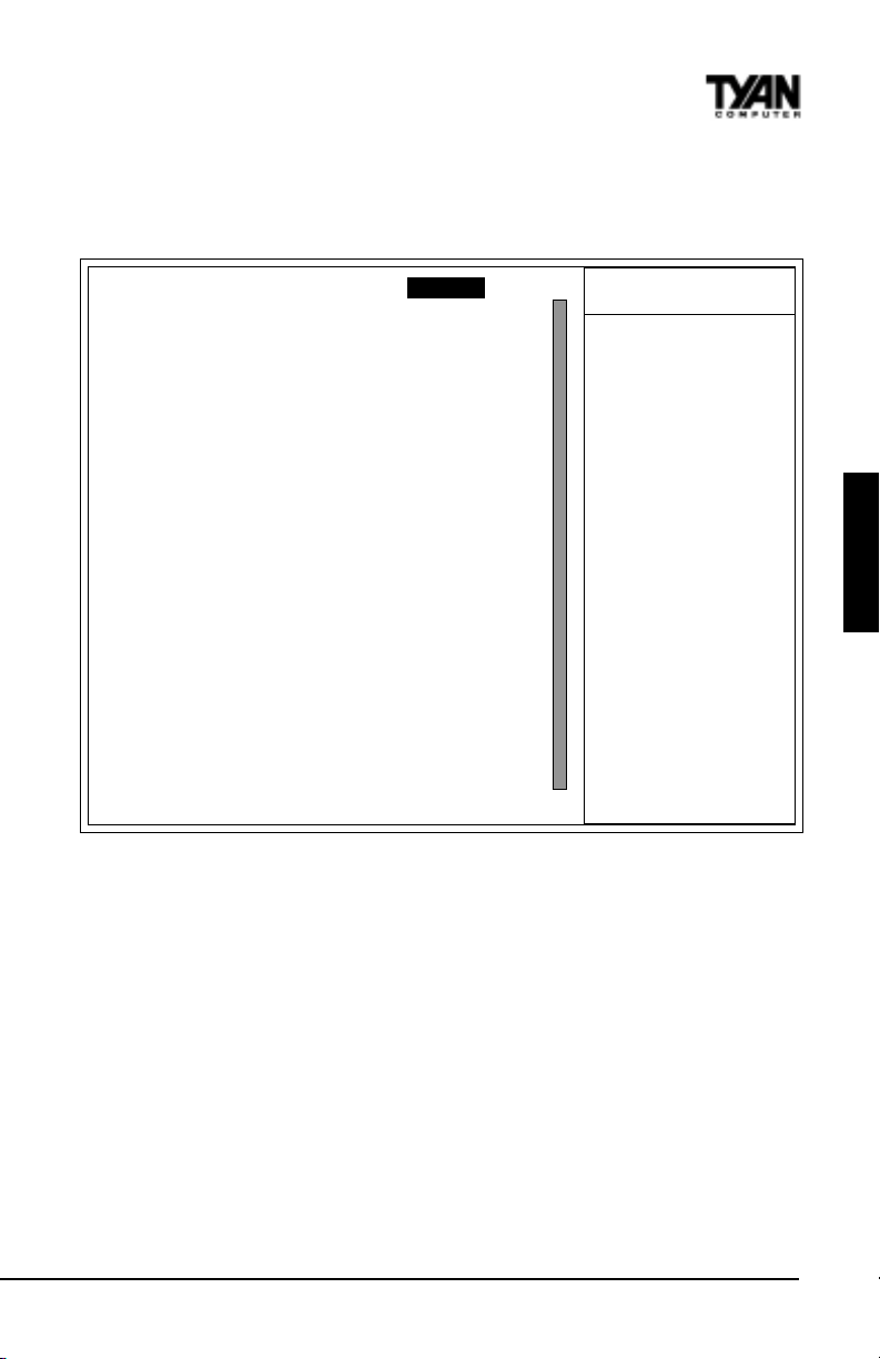
Advanced BIOS Features - Optimized Defaults
CMOS Setup Utility - Copyright (C) 1984-2000 Award Software
Standard CMOS Features
Virus Warning Disabled Item Help
CPU Internal Cache Enabled
External Cache Enabled Menu Level
CPU L2 Cache ECC Checking Enabled
Quick Power On Self Test Enabled Allows you to choose
First Boot Device Floppy the VIRUS warning
Second Boot Device HDD-0 feature for IDE Hard
Third Boot Device LS120 Disk boot sector
Boot Other Device Enabled protection. If this
Swap Floppy Drive Disabled function is enabled
Boot Up Floppy Seek Enabled and someone attempts
Boot Up NumLock Status On to write data into this
Gate A20 Option Fast area, BIOS will show a
Typematic Rate Setting Disabled warning message on
X Typematic Rate (Chars/Sec) 6 screen and alarm beep
X Typematic Delay (Msec) 250
Security Option Setup
OS Select For DRAM > 64MB Non-OS2
Video BIOS Shadow Enabled
C8000-CBFFF Shadow Disabled
CC000-CFFFF Shadow Disabled
D0000-D3FFF Shadow Disabled
D4000-D7FFF Shadow Disabled
D8000-DBFFF Shadow Disabled
DC000-CFFFF Shadow Disabled
↑ ↓ → ← :Move Enter:Select +/-/PU/PD:Value F10:Save ESC:Exit F1:General Help
F5:Previous Values F6:Fail-Safe Defaults F7:Optimized Defaults
▲
w
▲
BIOS
Virus Warning
When enabled, you receive a warning message if a program (specifically, a
virus) attempts to write to the boot sector or the partition table of the hard disk
drive. You should then run an anti-virus program. Keep in mind that this
feature protects only the boot sector, not the entire hard drive. Note: Many
disk diagnostic programs that access the boot sector table can trigger the virus
warning message. If you plan to run such a program, we recommend that you
first disable the virus warning.
CPU Internal Cache/External Cache
Cache memory is additional memory that is much faster than conventional
DRAM (system memory). CPUs from 486-type on up contain internal cache
S2380 Trinity K7
41
Page 42

Chapter 3
BIOS Configuration
memory, and most, but not all, modern PCs have additional (external) cache
memory. When the CPU requests data, the system transfers the requested data
from the main DRAM into cache memory, for even faster access by the CPU.
The External Cache field may not appear if your system does not have external
cache memory.
CPU L2 Cache ECC Checking
Enables Error Checking and correction (ECC) on the L2 cache onboard the
CPU.
Quick Power On Self Test
Select Enabled to reduce the amount of time required to run the power-on selftest (POST). A quick POST skips certain steps. We recommend that you
normally disable quick POST. Better to find a problem during POST than lose
data during your work.
Boot Sequence (First / Second / Third Boot Device)
The original IBM PCs loaded the operating system from drive A (floppy disk),
so IBM PC-compatible systems are designed to search for an operating system
first on drive A, and then on drive C (hard disk). However, modern computers
usually load the operating system from the hard drive, and may even load it
from a CD-ROM drive. The BIOS now offers a large number of boot devices
and boot sequence options.
Swap Floppy Drive
This option allows you to swap the floppy drives if more than one is installed.
It allows you to switch the A: and B: to make B: become A: .
Boot Up Floppy Seek
When Enabled, the BIOS tests (seeks) floppy drives to determine whether they
have 40 or 80 tracks. Only 360-KB floppy drives have 40 tracks; drives with 720
KB, 1.2 MB, and 1.44 MB capacity all have 80 tracks. Because very few modern
PCs have 40-track floppy drives, we recommend that you set this field to
Disabled to save time.
Boot Up NumLock Status
Toggle between On or Off to control the state of the NumLock key when the
system boots. When toggled On, the numeric keypad generates numbers
instead of controlling cursor operations.
http://www.tyan.com
42
Page 43

Gate A20 Option
Gate A20 refers to the way the system addresses memory above 1 MB
(extended memory). When set to Fast, the system chipset controls Gate A20.
When set to Normal, a pin in the keyboard controller controls Gate A20.
Setting Gate A20 to Fast improves system speed, particularly with OS/2 and
Windows.
Typematic Rate Setting
When Disabled, the following two items (Typematic Rate and Typematic
Delay) are irrelevant. Keystrokes repeat at a rate determined by the keyboard
controller in your system. When Enabled, you can select a typematic rate and
typematic delay.
Typematic Rate (Chars/Sec)
When the typematic rate setting is enabled, you can select a typematic rate
(the rate at which character repeats when you hold down a key) of 6, 8, 10,12,
15, 20, 24 or 30 characters per second.
Typematic Delay (Msec)
When the typematic rate setting is enabled, you can select a typematic delay
(the delay before key strokes begin to repeat) of 250, 500, 750 or 1000 milliseconds.
Security Option
If you have set a password, select whether the password is required every time
the System boots, or only when you enter Setup.
OS Select for DRAM > 64MB
Select OS2 only if you are running OS/2 operating system with greater than 64
MB of RAM on your system.
Video BIOS Shadow
Software that resides in a read-only memory (ROM) chip on a device is called
firmware. The EliteBIOS permits shadowing of firmware such as the system
BIOS, video BIOS, and similar operating instructions that come with some
expansion peripherals, such as, for example, a SCSI adaptor.
Shadowing copies firmware from ROM into system RAM, where the CPU can
read it through the 16-bit or 32-bit DRAM bus. Firmware not shadowed must
be read by the system through the 8-bit X-bus. Shadowing improves the
performance of the system BIOS and similar ROM firmware for expansion
peripherals, but it also reduces the amount of high memory (640 KB to 1 MB)
BIOS
S2380 Trinity K7
43
Page 44

Chapter 3
BIOS Configuration
available for loading device drivers, etc.
Enable shadowing into each section of memory separately. Many system
designers hardwire shadowing of the system BIOS and eliminate a System
BIOS Shadow option.
Video BIOS shadows into memory area C0000-C7FFF. The remaining areas
shown on the BIOS Features Setup screen may be occupied by other expansion card firmware. If an expansion peripheral in your system contains ROMbased firmware, you need to know the address range the ROM occupies to
shadow it into the correct area of RAM.
44
http://www.tyan.com
Page 45
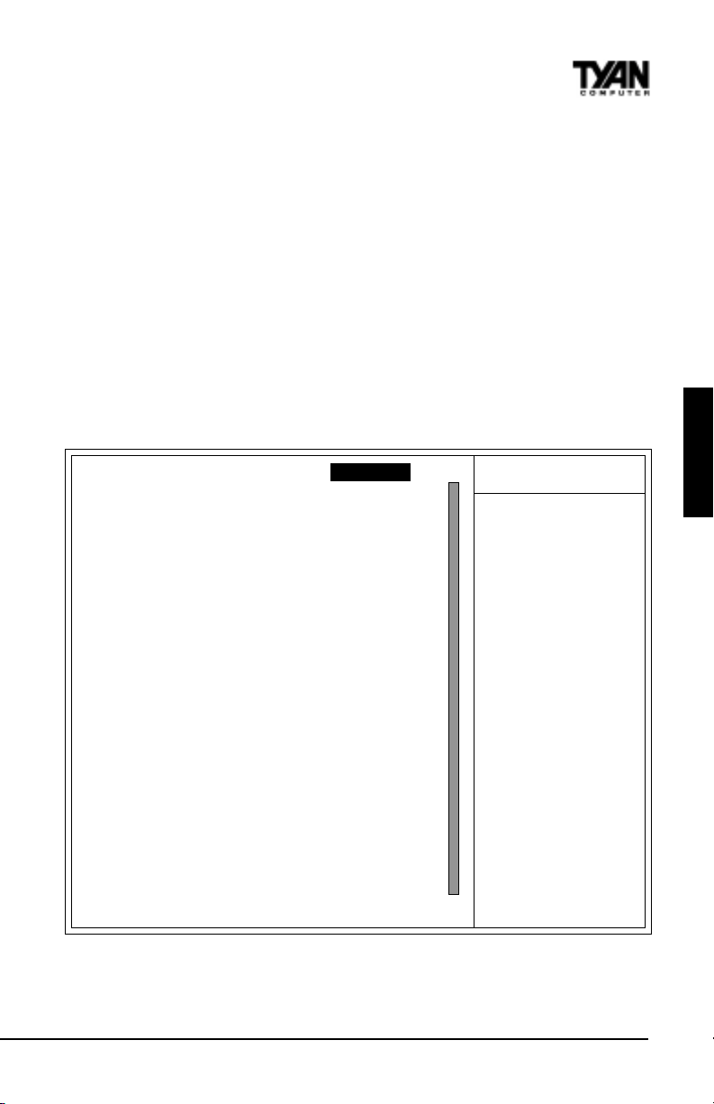
Advanced Chipset Features
This section describes features of the VIA KX-133 chipset.
Advanced Options
The parameters in this screen are for system designers, service personnel, and
technically competent users only. Do not reset these values unless you
understand the consequences of your changes. Note: This chapter describes
all fields offered by Award Software in this screen. Your system board designer
may omit or modify some fields.
Chipset Features Setup - Fail-Safe Default Settings
CMOS Setup Utility - Copyright (C) 1984-2000 Award Software
Advanced Chipset Features
Bank 0/1 DRAM Timing SDRAM 10ns Item Help
Bank 2/3 DRAM Timing SDRAM 10ns
Bank 4/5 DRAM Timing SDRAM 10ns Menu Level
SDRAM Cycle Length 3
DRAM Clock Host CLK
Memory Hole Disabled
P2C/C2P Concurrency Enabled
Fast R-W Turn Around Disabled
System BIOS Cacheable Disabled
Video RAM Cacheable Disabled
AGP Aperature Size 64M
AGP-4X Mode Enabled
AGP Driving Control Auto
X AGP Driving Value DA
K7 CLK_CTL Select Default
OnChip USB Enabled
USB Keyboard Support Disabled
OnChip Sound Auto
CPU to PCI Write Buffer Enabled
PCI Dynamic Bursting Disabled
PCI Master 0 WS Write Enabled
PCI Delay Transaction Disabled
PCI#2 Access #1 Retry Disabled
AGP Master 1 WS Write Disabled
AGP Master 1 WS Read Disabled
Memory Parity/ECC Check Disabled
▲
w
▲
BIOS
↑ ↓ → ← :Move Enter:Select +/-/PU/PD:Value F10:Save ESC:Exit F1:General Help
F5:Previous Values F6:Fail-Safe Defaults F7:Optimized Defaults
S2380 Trinity K7
45
Page 46
Chapter 3
BIOS Configuration
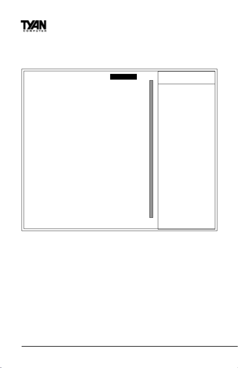
Chipset Features Setup - Optimized Default Settings
CMOS Setup Utility - Copyright (C) 1984-2000 Award Software
Advanced Chipset Features
Bank 0/1 DRAM Timing SDRAM 10ns Item Help
Bank 2/3 DRAM Timing SDRAM 10ns
Bank 4/5 DRAM Timing SDRAM 10ns Menu Level
SDRAM Cycle Length 3
DRAM Clock Host CLK
Memory Hole Disabled
P2C/C2P Concurrency Enabled
Fast R-W Turn Around Disabled
System BIOS Cacheable Disabled
Video RAM Cacheable Disabled
AGP Aperature Size 64M
AGP-4X Mode Enabled
AGP Driving Control Auto
X AGP Driving Value DA
K7 CLK_CTL Select Optimal
OnChip USB Enabled
USB Keyboard Support Disabled
OnChip Sound Auto
CPU to PCI Write Buffer Enabled
PCI Dynamic Bursting Enabled
PCI Master 0 WS Write Enabled
PCI Delay Transaction Enabled
PCI#2 Access #1 Retry Disabled
AGP Master 1 WS Write Disabled
AGP Master 1 WS Read Disabled
Memory Parity/ECC Check Disabled
↑ ↓ → ← :Move Enter:Select +/-/PU/PD:Value F10:Save ESC:Exit F1:General Help
F5:Previous Values F6:Fail-Safe Defaults F7:Optimized Defaults
▲
w
▲
Bank 0/1, 2/3, 4/5 DRAM Timing
The system board designer must select the proper value for these fields,
according to the specifications of the installed DRAM chips. Turbo mode
reduces CAS access time by 1 clock tick.
SDRAM Cycle Length
This field sets the CAS latency timing.
DRAM Clock
Allows you to set the memory clock speed to either 66MHz or equal to the
CPU clock speed, depending on your memory speed.
http://www.tyan.com
46
Page 47

Memory Hole
This option specifies the location of an area of memory that cannot be
addressed on the ISA bus. The settings are Disabled, 512KB-64KB, or 15MB16MB.
P2C/C2P Concurrency
By enabling this function the PCI/AGP Master to CPU Cycle can be concurrent
if the Host CPU is performing R/W access to the PCI or slave devices.
Fast Read Write turn-around
If Enabled, it reduces the turn around time for a memory read which is followed
by a memory write consecutively.
System BIOS Cacheable
If Enabled, results in better system performance by permitting caching of the
system BIOS ROM at F0000h-FFFFFh. Any program which tries to write to this
memory area, however, may cause a system error.
Video RAM Cacheable
Increases video performance by caching video memory.
AGP Aperture Size
Select the size of the Accelerated Graphics Port (AGP) aperture. The aperture is
a portion of the PCI memory address range dedicated for graphics memory
address space. Host cycles that hit the aperture range are forwarded to the
AGP without any translation. See www.agpforum.org for AGP information.
AGP-4x Mode
Enables the 4X AGP mode for higher AGP throughput. A 4X AGP graphics
card is required to enable this function.
Due to Tyans commitment to advanced technologies and first to market, not
all high performance 4X AGP graphics cards are compatible w/ our S2380 at the
time of print, please go to our web site for the latest update.
AGP Driving Control/Value
This sets the Driving Control value of the 4x AGP video card. Default settings
are set to Auto/ DA.
BIOS
AGP Fast Write
This function allows the AGP port to function at a increased rate. Enable this
function to allow faster graphics performance.
S2380 Trinity K7
47
Page 48

Chapter 3
BIOS Configuration
K7 CLK-CTL Select
This function sets the K7 clock controller. This setting should remain as
Optimal and should not be adjusted.
OnChip USB
The chipset contains an integrated USB controller. Select Enabled if you have
USB peripherals.
USB Keyboard Support
Select Enabled if your system contains a Universal Serial Bus (USB) controller
and you have a USB keyboard.
OnChip Sound
Integrated Audio is built into the KX-133 southbridge. Use this setting to
enable/disable the onboard sound feature.
CPU to PCI Write Buffer
When this field is Enabled, writes from the CPU to the PCI bus are buffered to
compensate for the speed differences between the CPU and the PCI bus.
When Disabled, the writes are not buffered and the CPU must wait until the
write is complete before starting another write cycle.
PCI Dynamic Bursting
When Enabled, every write transaction goes to the write buffer. Burstable
transactions then burst on the PCI bus; nonburstable transactions do not.
PCI Master 0 WS Write
When this field is Enabled, writes to the PCI bus are executed with zero wait
states.
PCI Delay Transaction
The chipset has an embedded 32-bit posted write buffer to support delay
transaction cycles. Select Enabled to support compliance with PCI specification version 2.1.
PCI#2 Access #1 Retry
Select Enabled to rotate priority of PCI masters.
AGP Master 1 WS Write / Read
Select Enabled to add one clock tick to AGP write operations.
http://www.tyan.com
48
Page 49
Memory Parity / ECC Check
Select Enabled, Disabled, or Auto. In Auto mode, the BIOS enables memory
checking automatically when it detects the presence of ECC or parity DRAM.
Integrated Peripherals
Note: This chapter describes all fields offered by Award Software in this
screen. Your system board designer may omit or modify some fields.
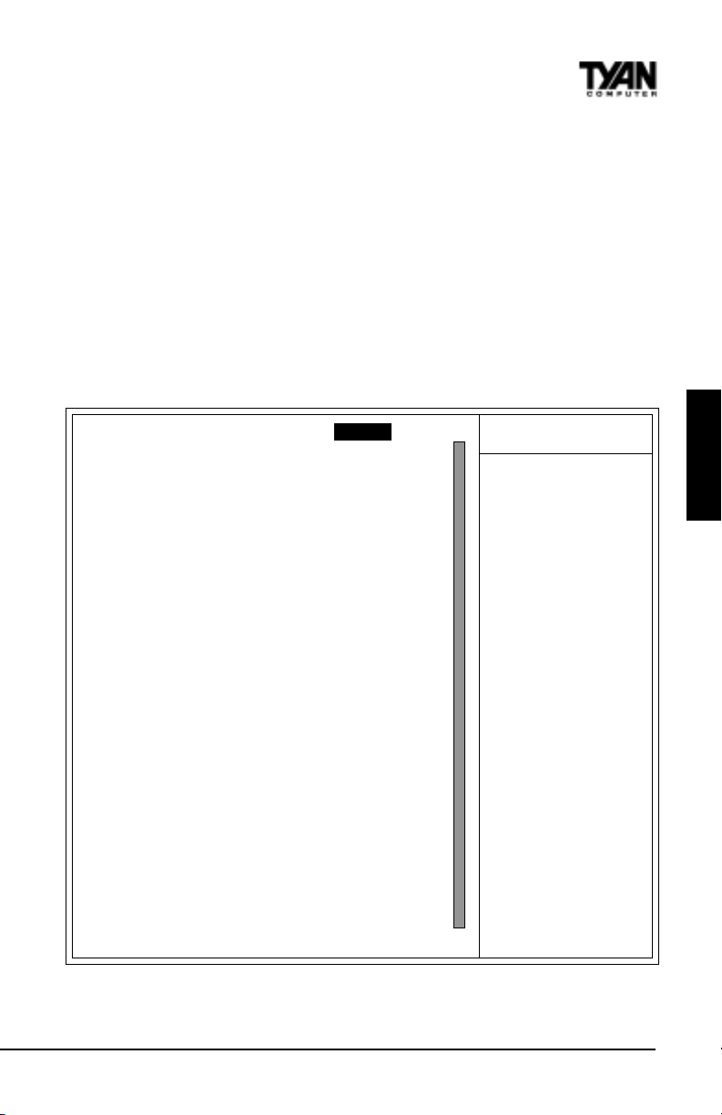
Integrated Peripherals - Fail-Safe Default Settings
CMOS Setup Utility - Copyright (C) 1984-2000 Award Software
Integrated Peripherals
OnChip IDE Channel0 Enabled Item Help
OnChip IDE Channel1 Enabled
IDE Prefetch Mode Disabled Menu Level
Primary Master PIO Auto
Primary Slave PIO Auto
Secondary Master PIO Auto
Secondary Slave PIO Auto
Primary Master UDMA Disable
Primary Slave UDMA Disable
Secondary Master UDMA Disable
Secondary Slave UDMA Disable
Init Display First PCI Slot
IDE HDD Block Mode Disabled
Onboard FDD Controller Enabled
Onboard Serial Port 1 3F8/IRQ4
Onboard Serial Port 2 2F8/IRQ3
UART 2 Mode Standard
X IR Function Duplex Half
X TX,RX inverting enable No, Yes
Onboard Parallel Port 378/IRQ7
Onboard Parallel Mode Normal
X ECP Mode Use DMA 3
X Parallel Port EPP Type EPP1.9
Sound Blaster Disabled
SB I/O Base Address 220H
SB IRQ SElect IRQ 5
SB DMA Select DMA 1
MPU-401 Disabled
MPU-401 I/O Address 330-333H
Game Port (200-207H) Enabled
▲
▲
BIOS
w
↑ ↓ → ← :Move Enter:Select +/-/PU/PD:Value F10:Save ESC:Exit F1:General Help
F5:Previous Values F6:Fail-Safe Defaults F7:Optimized Defaults
S2380 Trinity K7
49
Page 50
Chapter 3
BIOS Configuration
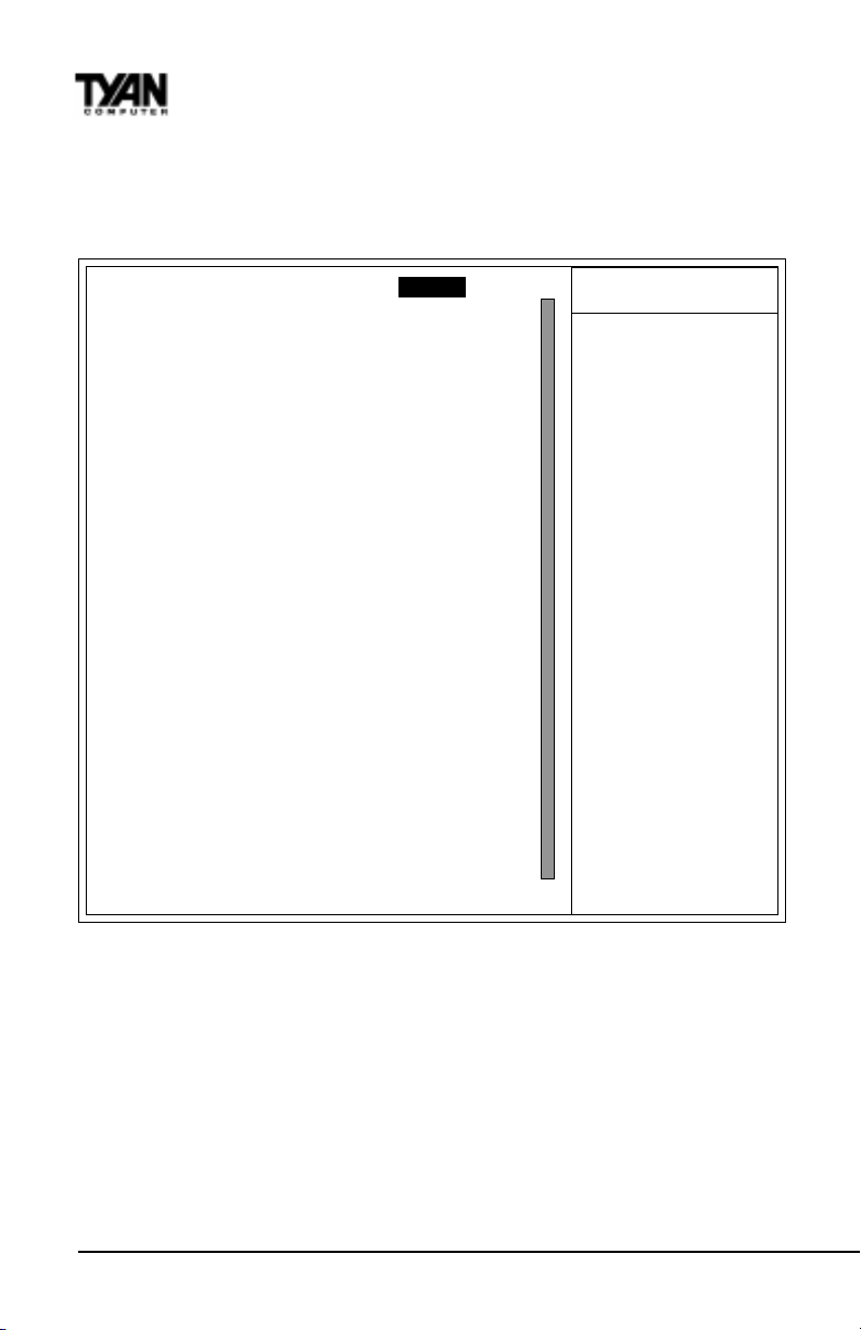
Integrated Peripherals - Optimized Default Settings
CMOS Setup Utility - Copyright (C) 1984-2000 Award Software
Integrated Peripherals
OnChip IDE Channel0 Enabled Item Help
OnChip IDE Channel1 Enabled
IDE Prefetch Mode Enabled Menu Level
Primary Master PIO Auto
Primary Slave PIO Auto
Secondary Master PIO Auto
Secondary Slave PIO Auto
Primary Master UDMA Auto
Primary Slave UDMA Auto
Secondary Master UDMA Auto
Secondary Slave UDMA Auto
Init Display First PCI Slot
IDE HDD Block Mode Enabled
Onboard FDD Controller Enabled
Onboard Serial Port 1 3F8/IRQ4
Onboard Serial Port 2 2F8/IRQ3
UART 2 Mode Standard
X IR Function Duplex Half
X TX,RX inverting enable No, Yes
Onboard Parallel Port 378/IRQ7
Onboard Parallel Mode Normal
X ECP Mode Use DMA 3
X Parallel Port EPP Type EPP1.9
MPU-401 Disabled
MPU-401 I/O Address 330-333H
Game Port (200-207H) Enabled
▲
▲
w
↑ ↓ → ← :Move Enter:Select +/-/PU/PD:Value F10:Save ESC:Exit F1:General Help
F5:Previous Values F6:Fail-Safe Defaults F7:Optimized Defaults
On-Chip IDE Channel 0/1
This chipset contains a PCI IDE interface with support for two IDE channels.
Select Enabled to activate the primary and/or secondary onboard IDE interface. Select Disabled to deactivate this interface, if you install a primary and/or
secondary add-in IDE interface.
http://www.tyan.com
50
Page 51

IDE Prefetch Mode
The onboard IDE drive interface supports IDE prefetching for faster drive
accesses. If you install a primary and/or secondary add-in IDE interface, set
this field to Disabled if the interface does not support prefetching.
IDE Primary/Secondary Master/Slave PIO
The four IDE PIO (Programmed Input/Output) fields let you set a PIO mode (0-
4) for each of up to four IDE devices that the internal PCI IDE interface
supports. Modes 0 through 4 provide successively increased performance. In
Auto mode, the system automatically determines the best mode for each
device.
IDE Primary/Secondary Master/Slave UDMA
UDMA (Ultra DMA) is a DMA data transfer protocol that utilizes ATA
commands and the ATA bus to allow DMA commands to transfer data at a
maximum burst rate of 66 MB/s. When you select Auto in the four IDE UDMA
fields (for each of up to four IDE devices that the internal PCI IDE interface
supports), the system automatically determines the optimal data transfer rate
for each IDE device.
Init Display First
Select the type of display adapter used in your system.
IDE HDD Block Mode
Block mode is also called block transfer, multiple commands, or multiple sector
read/write. If your IDE hard drive supports block mode (most new drives do),
select Enabled for automatic detection of the optimal number of block read/
writes per sector the drive can support.
Onboard FDC Controller
Select Enabled if your system has a floppy disk controller (FDC) installed on
the system board and you wish to use it. If you install an add-in FDC or the
system has no floppy drive, select Disabled in this field.
Onboard Serial Port 1/ 2
Select a logical COM port address and corresponding interrupt for the first and
second serial ports. The second serial port offers infrared options in the next
field.
BIOS
S2380 Trinity K7
51
Page 52

Chapter 3
BIOS Configuration
UART 2 Mode
Select an operating mode for the second serial port:
dradnatStroplairesC232-SR
RISPHtropderarfnilairestnailpmocADrI
RIKSAtropderarfnideyektfihsedutilpmA
Onboard Parallel Port
Select a logical LPT port address and corresponding interrupt for the physical
parallel port.
Onboard Parallel Mode
Select a mode for the onboard parallel port.
MPU-401
Select Enabled to configure the MPU-401 interface.
MPU-401 I/O Address
Select a base I/O address for the MPU-401 interface
Game Port (200-207H)
In order for the Game port to function, this setting must remain enabled.
http://www.tyan.com
52
Page 53
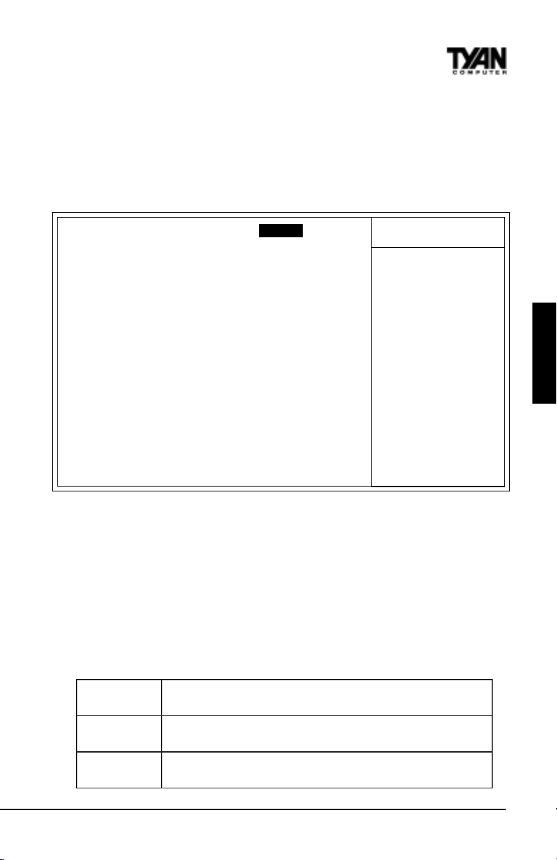
Power Management Setup
Power Management Setup - Fail-Safe and Optimized Default Settings
CMOS Setup Utility - Copyright (C) 1984-2000 Award Software
Power Management Setup
ACPI Function Enabled Item Help
w
Power Management Press Enter
ACPI Suspend Type S1(POS) Menu Level
Video Off Option Suspend -> Off
Video Off Method V/H SYNC+Blank
MODEM Use IRQ 3
Soft-Off by PWRBTN Instant-Off
State After Power Failure Auto
w
Wake Up Events Press Enter
↑ ↓ → ← :Move Enter:Select +/-/PU/PD:Value F10:Save ESC:Exit F1:General Help
F5:Previous Values F6:Fail-Safe Defaults F7:Optimized Defaults
w
BIOS
ACPI Function
Enable or disable Advanced Configuration Power Interface.
Power Management
This option allows you to select the type (or degree) of power saving for Doze,
Standby, and Suspend modes. See the section PM Timers for a brief description of each mode. This table describes each power management mode:
gnivasxaM
enifeDresU
gnivaSniM
S2380 Trinity K7
.edomhcaenietunim1
sremiTMPehtnisdoireptuo-emittceleS.yllaudividniedomhcaeteS
.gniwollof,noitces
.)evirddraheht
53
sidoirepytivitcanI.sUPCLSrofelbaliavaylnO.sgnivasrewopmumixaM
tpecxe(edomhcaeniruoh1sidoirepytivitcanI.sgnivasrewopmuminiM
Page 54

Chapter 3
BIOS Configuration
(Power Management option - Fail-safe and Optimized Default Settings)
CMOS Setup Utility - Copyright (C) 1984-2000 Award Software
Power Management
Power Management User Define Item Help
HDD Power Down Disable
Suspend Mode Disable Menu Level
w
↑ ↓ → ← :Move Enter:Select +/-/PU/PD:Value F10:Save ESC:Exit F1:General Help
F5:Previous Values F6:Fail-Safe Defaults F7:Optimized Defaults
HDD Power Down
After the selected period of drive inactivity (1 to 15 minutes), the hard disk
drive powers down while all other devices remain active.
Suspend Mode
After the selected period of system inactivity (1 minute to 1 hour), all devices
except the CPU shut off.
ACPI Suspend Type
Select the type of Power management used when the system goes into
standby. The choices are S1 POS or S3 STR. Default is S1.
http://www.tyan.com
54
Page 55

Video Off Option
Selects the power-saving modes during which the monitor goes blank.
nOsyawlA.sedomgnivas-rewopgnirudnosniamerrotinoM
ffO>--dnepsuS.edomdnepsuSsretnemetsysnehwdeknalbrotinoM
ffO>--sedoMllA.edomgnivas-rewopynasretnemetsysnehwdeknalbrotinoM
Video Off Method
Determines the manner in which the monitor is blanked. The Blank Screen
option will let the system BIOS blank the screen when disabling video. V/H
sync+Blank will allow the system BIOS to turn off the V-SYNC and H-SYNC
signals running from the VGA card to the monitor.
H/V
knalB+CNYS
troppuSSMPD
neercSknalB.reffuboedivehtotsknalbsetirwylnometsyS
.reffuboedivehtotsknalb
.seulavtnemeganamrewopoedivtcelesot
setirwdnastropnoitazinorhcnyslatnozirohdnalacitrevffosnrutmetsyS
tnemeganaMrewoPyalpsiDehtstroppusrotinomruoyfinoitposihttceleS
sdradnatSscinortcelEoediVehtfodradnats)SMPD(gnilangiS
metsysbusoedivruoyrofdeilppuserawtfosehtesU.)ASEV(noitaicossA
Modem Use IRQ
If Modem Ring Resume is Enabled, it is possible to wake the system by dialing
in to it. This field determines which IRQ will be monitored for the incoming call.
BIOS
Soft-Off by PWRBTN
When you select Instant Off or Delay 4 Sec., turning the system off with the
on/off button places the system in a very low power usage state, either
immediately or after 4 seconds, with only enough circuitry receiving power to
detect wake-up event activity.
PM Control by APM
If Advanced Power Management (APM) is installed on your system, selecting
Yes gives better power savings.
State After Power Failure
This function enables the computer to power up or down after a sudden power
interuption. If the setting is set to OFF, the computer will stay off even if the
power is resumed. If it is set to On, the computer will power on when power is
restored.
S2380 Trinity K7
55
Page 56
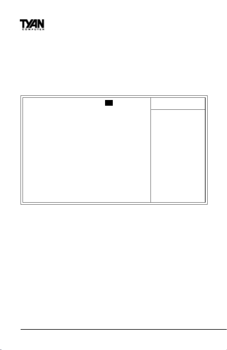
Chapter 3
BIOS Configuration
Wake Up Events
A power management (PM) event awakens the system from, or resets activity
timers for, Suspend mode.
(Wake Up Events option - Fail-safe and Optimized Default Settings)
CMOS Setup Utility - Copyright (C) 1984-2000 Award Software
Wake Up Events
VGA OFF Item Help
LPT & COM LPT/COM
HDD & FDD ON Menu Level
PCI Master OFF
Wake Up On LAN/Ring Disabled
RTC Alarm Resume Disabled
X Date (of Month) 0
X Resume Time (hh:mm:ss) 0 0 0
w
IRQs Activity Monitoring Press Enter
w
↑ ↓ → ← :Move Enter:Select +/-/PU/PD:Value F10:Save ESC:Exit F1:General Help
F5:Previous Values F6:Fail-Safe Defaults F7:Optimized Defaults
VGA
When On, any video activity is a PM event.
LPT & COM
Select none, or one or more, ports whose activity is a PM event.
HDD & FDD
When On, any hard drive or floppy drive activity is a PM event.
PCI Master
When On, any PCI card activity is a PM event.
http://www.tyan.com
56
Page 57
Wake Up on LAN
This feature allows remote power up through a LAN connection when used in
conjunction with a Wake on LAN compliant network adapter and appropriate
software.
RTC Alarm Resume
When Enabled, you can set the date and time at which the RTC (real-time
clock) alarm awakens the system from Suspend mode.
IRQs Activity Monitoring
Please refer to the screen shot below for the options in IRQ Activity Monitoring.
(IRQs Activity Monitoring - Fail-safe and Optimized Default Settings)
CMOS Setup Utility - Copyright (C) 1984-2000 Award Software
IRQs Activity Monitoring
Primary INTR ON Item Help
IRQ3 (COM 2) Enabled
IRQ4 (COM 1) Enabled Menu Level
IRQ5 (LPT 2) Enabled
IRQ6 (Floppy Diske) Enabled
IRQ7 (LPT 1) Enabled
IRQ8 (RTC Alarm) Disabled
IRQ9 (IRQ2 Redir) Disabled
IRQ10 (Reserved) Disabled
IRQ11 (Reserved) Disabled
IRQ12 (PS/2 Mouse) Enabled
IRQ13 (Coprocessor) Enabled
IRQ14 (Hard Disk) Enabled
IRQ15 (Reserved) Disabled
↑ ↓ → ← :Move Enter:Select +/-/PU/PD:Value F10:Save ESC:Exit F1:General Help
F5:Previous Values F6:Fail-Safe Defaults F7:Optimized Defaults
w
ww
BIOS
S2380 Trinity K7
57
Page 58

Chapter 3
BIOS Configuration
Primary INTR
A system peripheral signals that it wants to gain the attention of the operating
system by sending an interrupt request. When the system is in Suspend mode,
IRQ activity can cause a Primary or Secondary wake-up. When Primary INTR is
On, the IRQs in the above fields can be configured as Primary, Secondary, or
Disabled.
IRQn
The following is a list of IRQs (Interrupt Request Lines) assigned to common
system peripherals.
IRQ3 (COM2) IRQ10 (Reserved)
IRQ4 (COM1) IRQ11 (Reserved)
IRQ5 (LPT2) IRQ12 (PS/2 Mouse)
IRQ6 (Floppy Disk) IRQ13 (Coprocessor)
IRQ7 (LPT1) IRQ14 (Hard Disk)
IRQ8 (RTC Alarm) IRQ15 (Reserved)
IRQ9 (IRQ2 Redir)
58
http://www.tyan.com
Page 59
PnP/PCI Configurations
Note: This chapter describes all fields offered by Award Software in this
screen. Your system board designer may omit or modify some fields.
PnP/PCI Configurations - Fail-Safe and Optimized Default Settings
CMOS Setup Utility - Copyright (C) 1984-2000 Award Software
PnP/PCI Configurations
PNP OS Installed NO Item Help
Reset Configuration Data Disabled
Menu Level
Resources Controlled By Auto(ESCD)
X IRQ Resources Press Enter Select Yes if you are
X DMA Resources Press Enter using a Plug and Play
capable operating
PCI/VGA Palette Snoop Disabled system. Select No if
Assign IRQ For VGA Enabled you need the BIOS to
Assign IRQ For USB Enabled configure non-Boot
devices
w
BIOS
↑ ↓ → ← :Move Enter:Select +/-/PU/PD:Value F10:Save ESC:Exit F1:General Help
F5:Previous Values F6:Fail-Safe Defaults F7:Optimized Defaults
PNP OS Installed
Select Yes if the system operating environment is Plug-and-Play aware (e.g.,
Windows 95).
Reset Configuration Data
Normally, you leave this field Disabled. Select Enabled to reset Extended
System Configuration Data (ESCD) when you exit Setup if you have installed a
new add-on and the system reconfiguration has caused such a serious conflict
that the operating system cannot boot.
S2380 Trinity K7
59
Page 60

Chapter 3
BIOS Configuration
Resources Controlled By
The Plug and Play EliteBIOS can automatically configure all the boot and Plug
and Play-compatible devices. If you select Auto, all the interrupt request (IRQ)
and DMA assignment fields disappear, because the BIOS automatically
assigns them.
IRQ Resources (IRQ-n Assigned to)
When resources are controlled manually, assign each system interrupt as one
of the following types, depending on the type of device using the interrupt:
Legacy ISA: Devices compliant with the original PC AT bus
specification, requiring a specific interrupt (such as IRQ4 for serial
port 1).
PCI/ISA PnP: Devices compliant with the Plug and Play standard,
whether designed for PCI or ISA bus architecture.
DMA Resources (DMA-n Assigned to)
When resources are controlled manually, assign each system DMA channel as
one of the following types, depending on the type of device using the
interrupt:
Legacy ISA: Devices compliant with the original PC AT bus
specification, requiring a specific DMA channel
PCI/ISA PnP: Devices compliant with the Plug and Play standard,
whether designed for PCI or ISA bus architecture.
PCI / VGA Palette Snoop
Please leave this field at Disabled.
Assign IRQ for VGA
Assign an IRQ number to your VGA adapter.
Assign IRQ For USB
Assign an IRQ number to your USB device / controller.
60
http://www.tyan.com
Page 61
User Password (Supervisor / User)
When you select this function, a message appears at the center of the screen:
ENTER PASSWORD:
Type the password, up to eight characters, and press Enter. Typing a password clears any previously entered password from CMOS memory. Now the
message changes:
CONFIRM PASSWORD:
Again, type the password and press Enter. To abort the process at any time,
press Esc.
In the Security Option item in the Advanced BIOS Features Setup screen,
select System or Setup:
BIOS
metsyS
puteS.puteSretneuoyrevenehwdrowssaparetnE
.puteS
retneuoyrevenehwdnastoobmetsysehtemithcaedrowssaparetnE
Note: To clear the password, simply press Enter when asked to enter a
password. Then the password function is disabled.
Flash Writer Utility
You can upgrade the BIOS on your motherboard by using the Flash Memory
Writer (FMW) utility. This utility can be downloaded from TYANs BBS and
from the TYAN website. The system BIOS is stored on a flash EEPROM chip
on the mainboard, which can be erased and reprogrammed by the FMW. The
following three files make up the FMW:
AWDFLASH.EXE The Flash Memory Writer utility for Award to
Award upgrade.
README.TXT A text file of instructions.
S71AWXX.BIN* The new BIOS file.
(*This file name is subject to change and can have either a .bin or .rom extension.)
The FMW records (or programs) a new BIOS onto the flash memory chip. You
S2380 Trinity K7
61
Page 62

Chapter 3
BIOS Configuration
cannot upgrade an Award BIOS to an AMI BIOS or vice-versa.
Note: You should always clear your CMOS after flashing a BIOS. This will clear
out any stray settings from your old BIOS which may have been carried over
from the flashing process. Most problems encountered after flashing a BIOS
will be solved by this simple procedure.
To reprogram the system BIOS, the CPU must be running in real mode. FMW
will not run if the CPU is operating in a protected or virtual mode. This means
that you cannot run it with Windows running or with any memory manager
software. You must disable any memory manager software before you can run
FMW. The easiest way to do this is as follows:
1) Boot your system from a bootable floppy disk with no CONFIG.SYS or
AUTOEXEC.BAT files, and then run FMW from a backup copy of your
support disk. You can make your back-up floppy bootable when you format it,
and use one disk for both purposes.
2) If you are using MS-DOS 6.x, you can use the feature that allows you to
bypass the CONFIG.SYS and AUTOEXEC.BAT files. You can access this
feature by pressing <F5> while the Starting MS-DOS... line is on the screen
during boot-up.
If you are uncertain whether or not you have a memory manager running, try
FMW. If it works, then there is no active memory manager on your system. If
you see a warning message about the CPU mode, follow the above directions
to get around the memory manager.
Once you have your CPU in real mode, you can run FMW. You can copy the
contents of the Flash directory to your hard drive, or you can run the utility
from a backup of the support floppy disk. Either way, make sure that the new
BIOS file is in the same directory as the FMW utility.
To start FMW, change to the Flash directory if you are not already in it.
Type awdflash at the DOS command line and press the <Enter> key. The
FMW utility screen will appear:
http://www.tyan.com
62
Page 63
FLASH MEMORY WRITER V3.0
Copyright(C) 1993, AWARD SOFTWARE, INC.
For VX/HX-2A59CT51 Date:4/13/98
File Name to Program:
Error Message:
Type in the whole file name, e.g. A61AW10.BIN, and confirm that you want
to program the BIOS. The utility will then Blank, Erase, and Program
the flash memory on the mainboard with the new BIOS file. You should
choose Yes to save the original system BIOS to a floppy diskette before
you program the new BIOS. This leaves you with a backup of your original
BIOS in case you need to re-install it. If you cannot successfully program the
new BIOS file for some reason, re-install your original BIOS from the backup
file. Remember, always reset the CMOS after flashing to a new BIOS (see
page 15).
BIOS
Warning: If you do not successfully install a complete BIOS file in the flash
memory on the mainboard, your system may not be able to boot. If this happens, it will require service by your system vendor. Follow the instructions in
this section precisely to avoid such an inconvenience.
S2380 Trinity K7
63
Page 64
Chapter 4
System Resources
chapter 4
System Resources
Beep Codes
Fatal errors, which halt the boot process, are communicated through a series of
audible beeps. Currently the only beep code indicated that a video error has
occured and the BIOS cannot initialize the video screen to display any
additional information. This beep code consists of a single long beep followed
by two short beeps. Any other beeps are probably a RAM problem
64
http://www.tyan.com
Page 65
Appendix
Glossary
ACPI (Advanced Configuration and Power Interface) is a power management
specification that allows the operating system to control the amount of power
distributed to the computers devices. Devices not in use can be turned off,
reducing unnecessary power expenditure.
AGP (Accelerated Graphics Port) is a PCI-based interface which was designed
specifically for demands of 3D graphics applications. The 32-bit AGP channel
directly links the graphics controller to the main memory. While the channel
runs at only 66MHz, it supports data transmission during both the rising and
falling ends of the clock cycle, yielding an effective speed of 133MHz.
AT was the original form factor of IBMs PC.
ATAPI (AT Attachment Packet Interface), also known as IDE or ATA, is a drive
implementation that includes the disk controller on the device itself. It allows
CD-ROMs and tape drives to be configured as master or slave devices, just
like hard drives.
AT X form factor was designed to replace the AT form factor. It improves on the
AT design by rotating the board ninety degrees, so that the IDE connectors
are closer to the drive bays, and the CPU is closer to the power supply and
cooling fan. The keyboard, mouse, serial, USB, and parallel ports are built in.
Bandwidth refers to carrying capacity. The greater the bandwidth, the more
data the bus, phone line, or other electrical path, can carry. Greater bandwidth,
S2380 Trinity K7
65
Page 66

Appendix
Glossary
then, also results in greater speed.
The BIOS (Basic Input/Output System) program resides in the ROM chip, and
provides the basic instructions for controlling your computers hardware. Both
the operating system and application software use BIOS routines to ensure
compatibility.
A buffer is a portion of RAM which is used to temporarily store data, usually
from an application, though it is also used when printing, and in most keyboard drivers. The CPU can manipulate data in a buffer before copying it, all at
once, to a disk drive. While this improves system performance--reading to or
writing from a disk drive a single time is much faster than doing so repeatedly-there is the possibility of losing your data should the system crash. Information stored in a buffer is temporarily stored, not permanently saved.
A bus is a data pathway. The term is used especially to refer to the connection
between the processor and system memory, and between the processor and
PCI or ISA local buses.
Bus mastering allows peripheral devices and IDEs to access the system
memory without going through the CPU (similar to DMA channels).
A cache is a temporary storage area for data that will be needed often by an
application. Using a cache lowers data access times, since the needed information is stored in the SRAM instead of in the slower DRAM. Note that the
cache is also much smaller than your regular memory: a typical cache size is
512KB, while you may have as much as 1GB of regular memory.
Cache size refers to the physical size of the cache onboard. This should not be
confused with the cacheable area, which is the total amount of memory which
can be scanned by the system in search of data to put into the cache. A typical
setup would be a cache size of 512KB, and a cacheable area of 512MB. In this
case, up to 512MB of the main memory onboard is capable of being cached.
However, only 512KB of this memory will be in the cache at any given moment.
Any main memory above 512MB could never be cached.
Closed and open jumpers Jumpers and jumper pins are active when they are
On or Closed, and inactive when they are Off or Open.
CMOS Complementary Metal-Oxide Semiconductors are chips that hold the
basic start-up information for the BIOS.
The COM port is another name for the serial port, which is so-called because it
http://www.tyan.com
66
Page 67

transmits the eight bits of a byte of data along one wire, and receives data on
another single wire (that is, the data is transmitted in serial form, one bit after
another). Parallel ports transmit the bits of a byte on eight different wires at the
same time (that is, in parallel form, eight bits at the same time).
DDR or Double Data Rate is a form of data transfer that is supported on both
ends of the clock cycle. DDR allows double the speed of the initial transfer
rate.
DIMM Dual In-line Memory Modules are a faster and more capacious form of
RAM than SIMMs, and do not need to be installed in pairs.
DIMM bank DIMM banks are sometimes called DIMM sockets, because the
physical slot and the logical unit are the same. That is, one DIMM module fits
into one DIMM socket, which is capable of acting as a memory bank.
DMA Direct Memory Access channels are similar to IRQs. DMA channels
allow hardware devices (like sound cards or keyboards) to access the main
memory without involving the CPU. This frees up CPU resources for other
tasks. As with IRQs, it is vital that you do not double up devices on a single
line. Plug and Play devices will take care of this for you.
In Doze mode, only the CPUs speed is slowed.
DRAM Dynamic RAM is a widely available, very affordable form of RAM
which has the unfortunate tendency to lose data if it is not recharged regularly
(every few milliseconds). This refresh requirement makes DRAM three to ten
times slower than non-recharged RAM such as SRAM.
GLOSSARY
EDO RAM (Extended Data-Out RAM) speeds access to memory locations by
assuming that memory addresses are static: the next time it looks for a bit of
data, it will be at the same spot, or one nearby.
EEPROM Electrically Erasable Programmable ROM, also called Flash BIOS, is
a ROM chip which can, unlike normal ROM, be updated. This allows you to
keep up with changes in the BIOS programs without having to buy a new chip.
TYANs BIOS updates can be found at http://www.tyan.com/html/drivers.html
ESCD (Extended System Configuration Data) is a format for storing informa-
tion about Plug and Play devices in the system BIOS. This information helps
properly configure the system each time it boots.
S2380 Trinity K7
67
Page 68

Appendix
Glossary
Firmware is low level software that controls the system hardware.
Form factor is an industry term for the size, shape, power supply type, and
external connector type of the PCB (personal computer board) or motherboard.
The standard form factors are the AT and ATX, although TYAN also makes
some Baby-AT boards.
A Global timer is an onboard hardware timer, such as the Real Time Clock.
Handshaking is a form of encryption. One system, typically the server, sends
an encryption scheme to another agent, typically a client. Thus, the clients
data is protected during transmittal to the server.
HDD stands for Hard Disk Drive.
H-SYNC controls the horizontal properties of the monitor.
IC (Integrated Circuit) is the formal name for the computer chip.
IDE Integrated Device (or Drive) Electronics is a simple, self-contained hard
drive interface. It can handle drives up to 8.4GB in size. Almost all IDEs sold
now are in fact Enhanced IDEs (EIDEs).
IDE INT (IDE Interrupt) is a hardware interrupt signal that goes to the IDE.
I/O Input/Output is the connection between your computer and another piece
of hardware (mouse, keyboard, etc.).
IRQ An Interrupt Request is an electronic request that runs from a hardware
device to the CPU. The interrupt controller assigns priorities to incoming
requests and delivers them to the CPU. It is important that there is only one
device hooked up to each IRQ line; doubling up devices on IRQ lines can lock
up your system. Happily, Plug and Play operating systems take care of these
details for you.
ISA stands for Industry Standard Architecture. ISA is a slower 8- or 16-bit BUS
(data pathway).
Latency is the amount of time that one part of a system spends waiting for
another part to catch up. This is most common when the system sends data
out to a peripheral device, and is waiting for the peripheral to send some data
back (peripherals tend to be slower than onboard system components).
http://www.tyan.com
68
Page 69
NVRAM ROM and EEPROM are both examples of Non-Volatile RAM, memory
that holds its data without power. DRAM, in contrast, is volatile.
OEMs (Original Equipment Manufacturers) like Compaq or IBM package other
companies motherboards and hardware inside their case and sell them.
The parallel port transmits the bits of a byte on eight different wires at the
same time (that is, in parallel form, eight bits at the same time).
PCI stands for Peripheral Component Interconnect. PCI is a 32-bit local bus
(data pathway) which is faster than the ISA bus. Local buses are those which
operate within a single system (as opposed to a network bus, which connects
multiple systems).
The PCI PIO (PCI Programmable Input/Output) modes are the data transfer
modes used by IDE drives. These modes use the CPU for data transfer (DMA
channels do not). PCI refers to the type of bus used by these modes to
communicate with the CPU.
PCI-to-PCI bridge allows you to connect multiple PCI devices onto one PCI
slot.
Pipeline burst SRAM is a fast secondary cache. It is used as a secondary
cache because SRAM is slower than SDRAM, but usually larger. Data is
cached first to the faster primary cache, and then, when the primary cache is
full, to the slower secondary cache.
GLOSSARY
Pipelining improves system performance by allowing the CPU to begin
executing a second instruction before the first is completed. A pipeline can be
likened to an assembly line, with a given part of the pipeline repeatedly
executing a set part of an operation on a series of instructions.
PM timers (Power Management timers) are software timers that count down
the number of seconds or minutes until the system times out and enters sleep,
suspend, or doze mode.
PnP is an acronym for Plug and Play, a design standard that has become
ascendant in the industry. Plug and Play devices require little set-up to use.
Novice end users can simply plug them into a computer that is running on a
Plug and Play-aware operating system (such as Windows 95), and go to work.
S2380 Trinity K7
69
Page 70

Appendix
Glossary
Devices and operating systems that are not Plug and Play require you to
reconfigure your system each time you add or change any part of your
hardware.
The term RAM (Random Access Memory), while technically referring to a type
of memory where any byte can be accessed without touching the adjacent
data, is often used to refer to the systems main memory. This memory is
available to any program running on the computer.
ROM (Read-Only Memory) is a storage chip which contains the BIOS (Basic
Input/Output System), the basic instructions required to boot the computer
and start up the operating system.
SDRAM (Synchronous Dynamic RAM) is so-called because it can keep two
sets of memory addresses open simultaneously. By transferring data alternately from one set of addresses, and then the other, SDRAM cuts down on
the delays associated with non-synchronous RAM, which must close one
address bank before opening the next.
The serial port is so called because it transmits the eight bits of a byte of data
along one wire, and receives data on another single wire (that is, the data is
transmitted in serial form, one bit after another).
SIMM Single In-line Memory Modules are the most common form of RAM.
They must be installed in pairs, and do not have the carrying capacity or the
speed of DIMMs.
SIMM bank/socket SIMM sockets are the physical slots into which you stick
SIMM modules. A pair of SIMM sockets form a SIMM bank, and act as a unit.
If only one socket is filled, the bank will not operate.
In Sleep/Suspend mode, all devices except the CPU shut down.
SRAM Static RAM, unlike DRAM, does not need to be refreshed in order to
prevent data loss. Thus, it is faster, and more expensive.
In Standby mode, the video and fixed disk drive shut down; all other devices
operate normally.
http://www.tyan.com
70
Page 71
UltraDMA/66 is a fast version of the old DMA channel. UltraDMA is also
called UltraATA. Without UltraDMA your system cannot take advantage of
the higher data transmission rates of the new UltraATA hard drives.
Universal Serial Bus or USB, is a versatile port. This one port type can
function as a serial, parallel, mouse, keyboard, or joystick port. It is fast
enough to support video transfer, and is capable of supporting up to 127
daisy-chained peripheral devices.
VGA (Video Graphics Array) is the PC video display standard.
V-SYNC controls the vertical properties of the monitor.
ZIF socket Zero Insertion Force sockets make it possible to insert CPUs
without damaging the sensitive pins. The CPU is lightly placed in an open ZIF
socket, and the metal lever pulled down. This shifts the processor over and
down, guiding it into place on the board.
GLOSSARY
S2380 Trinity K7
71
Page 72

Notice for the USA
Compliance Information Statement (Declaration of Conformity Procedure) DoC
FCC Part 15: This Device complies with Part 15 of the FCC Rules.
Operation is subject to the following conditions:
1) this device may not cause harmful interference, and
2) this device must accept any interference received including interference that
may cause undesired operation. If this equipment does cause harmful interference to radio or television reception, which can be determined by turning the
equipment off and on, the user is encouraged to try one or more of the
following measures:
• Reorient or relocate the receiving antenna.
• Increase the separation between the equipment and receiver.
• Plug the equipment into an outlet on a circuit different from
that of the receiver.
• Consult the dealer or an experienced radio/television
technician for help.
Notice for Canada
This apparatus complies with the Class B limits for radio interference as
specified in the Canadian Department of Communications Radio Interference
Regulations. (Cet appareil est conforme aux normes de Classe B d interference radio tel que spécifié par le Ministére Canadien des Communications
dans les réglements dinterférence radio.)
Notice for Europe (CE Mark)
This product is in conformity with the Council Directive 89/336/EEC, 92/31/EEC
(EMC).
CAUTION: Lithium Batteries included with this board. Danger of explosion if
battery is incorrectly replaced. Replace only with the same or equivalent type
recommended by manufacturer. Dispose of used batteries according to
manufacturer instructions.
Note: The joystick port maximum output rating is 9 amperes at 5 volts.
Document # D1395-100
http://www.tyan.com
72
 Loading...