

Tundra TSI308 User Manual

®
Tsi308™
TitlePage - 80D4000_MA001_02
HyperTransport-to-PCI-X Bridge
User Manual
Document Number: 80D4000_MA001_02
Document Status: Preliminary
Revision Date: September 2006
Tundra Semiconductor Corporation

Trademarks
TUNDRA is a registered trademark of Tundra Semiconductor Corporation (Canada, U.S., and U.K.). TUNDRA,
the Tundra logo, T si308, and Silicon Behind the Network, are trademarks of Tundra Semiconductor Corporation.
All other registered and unregistered marks (including trademarks, service marks and logos) are the property of
their respective owners. The absence of a mark identifier is not a representation that a particular product name is
not a mark.
Copyright
Copyright © September 2006 Tundra Semiconductor Corporation. All rights reserved.
Published in Canada
This document contains info rmat ion t hat i s pr opri eta ry to Tundra and may be us ed f or non -comm e rcia l pu rpo ses
within your organization in support of Tundra products. No other use or transmission of all or any part of this
document is permitted without written permission from Tundra, and must include all copyright and other
proprietary notices. Use or transmission of all or any part of this document in violation of any applicable
Canadian or other legislation is hereby expressly prohibited. User obtains no rights in the information or in any
product, process, technology or trademark which it includes or describes, and is expressly prohibited from
modifying the information or creating derivative works without the express written consent of Tundra.
Disclaimer
Tundra assumes no respo nsibility for the accuracy o r completeness of the information presented, which is subject
to change without notice. Tundra products may cont ain design defect s or error s known as er rata which ma y cause
the product to deviate from published specifications. Current characterized errata are available on request. In no
event will Tundra be liable for any direct, indirect, special, incidental or consequential damages, including lost
profits, lost business or lost data, resulting from the use of or reliance upon th e info rmation, whether or not
Tundra has been advised of the possibility of such damages. The information contained in this document does
not affect or change Tundra’s product warranties.
Mention of non-Tundra products or services is for information purposes only and constitutes neither an
endorsement nor a recommendation.

®
Contact Information
Text inset to be placed
3
Tundra Semiconductor Corporation
www.tundra.com
Tsi308 User Manual
80D4000_MA001_02

4
Tsi308 User Manual
80D4000_MA001_02
Tundra Semiconductor Corporation
www.tundra.com

®
Corporate Profile
Text inset to be inserted later.
5
Tundra Semiconductor Corporation
www.tundra.com
Tsi308 User Manual
80D4000_MA001_02

6
Tsi308 User Manual
80D4000_MA001_02
Tundra Semiconductor Corporation
www.tundra.com

®
Contents
Contact Information. . . . . . . . . . . . . . . . . . . . . . . . . . . . . . . . . . . . . . . . . . . . . . . . . . . . . . 3
Corporate Profile . . . . . . . . . . . . . . . . . . . . . . . . . . . . . . . . . . . . . . . . . . . . . . . . . . . . . . . . 5
About this Document. . . . . . . . . . . . . . . . . . . . . . . . . . . . . . . . . . . . . . . . . . . . . . . . . . . . 17
Scope . . . . . . . . . . . . . . . . . . . . . . . . . . . . . . . . . . . . . . . . . . . . . . . . . . . . . . . . . . . . . . . . . . . . . . . . . . . 17
Document Conventions . . . . . . . . . . . . . . . . . . . . . . . . . . . . . . . . . . . . . . . . . . . . . . . . . . . . . . . . . . . . . 17
Related Information . . . . . . . . . . . . . . . . . . . . . . . . . . . . . . . . . . . . . . . . . . . . . . . . . . . . . . . . . . . . . . . . 19
Revision History . . . . . . . . . . . . . . . . . . . . . . . . . . . . . . . . . . . . . . . . . . . . . . . . . . . . . . . . . . . . . . . . . . . 19
1. Functional Description . . . . . . . . . . . . . . . . . . . . . . . . . . . . . . . . . . . . . . . . . . . . . . 21
1.1 Overview . . . . . . . . . . . . . . . . . . . . . . . . . . . . . . . . . . . . . . . . . . . . . . . . . . . . . . . . . . . . . . . . . . . 22
1.2 Features. . . . . . . . . . . . . . . . . . . . . . . . . . . . . . . . . . . . . . . . . . . . . . . . . . . . . . . . . . . . . . . . . . . . . 23
1.2.1 General features. . . . . . . . . . . . . . . . . . . . . . . . . . . . . . . . . . . . . . . . . . . . . . . . . . . . . . 23
7
1.3 HyperTransport Interface . . . . . . . . . . . . . . . . . . . . . . . . . . . . . . . . . . . . . . . . . . . . . . . . . . . . . . . 24
1.4 PCI-X Interface. . . . . . . . . . . . . . . . . . . . . . . . . . . . . . . . . . . . . . . . . . . . . . . . . . . . . . . . . . . . . . . 25
1.4.1 PCI-X Master. . . . . . . . . . . . . . . . . . . . . . . . . . . . . . . . . . . . . . . . . . . . . . . . . . . . . . . . 25
1.4.2 PCI-X Slave. . . . . . . . . . . . . . . . . . . . . . . . . . . . . . . . . . . . . . . . . . . . . . . . . . . . . . . . . 26
1.4.3 PCI-X Arbiter. . . . . . . . . . . . . . . . . . . . . . . . . . . . . . . . . . . . . . . . . . . . . . . . . . . . . . . . 26
1.5 Interrupt Controller. . . . . . . . . . . . . . . . . . . . . . . . . . . . . . . . . . . . . . . . . . . . . . . . . . . . . . . . . . . . 27
1.6 Interface Levels . . . . . . . . . . . . . . . . . . . . . . . . . . . . . . . . . . . . . . . . . . . . . . . . . . . . . . . . . . . . . . 27
1.7 Clocking . . . . . . . . . . . . . . . . . . . . . . . . . . . . . . . . . . . . . . . . . . . . . . . . . . . . . . . . . . . . . . . . . . . . 28
1.8 Reset . . . . . . . . . . . . . . . . . . . . . . . . . . . . . . . . . . . . . . . . . . . . . . . . . . . . . . . . . . . . . . . . . . . . . . . 28
2. Interface Operation . . . . . . . . . . . . . . . . . . . . . . . . . . . . . . . . . . . . . . . . . . . . . . . . . 29
2.2 HyperTransport Interface . . . . . . . . . . . . . . . . . . . . . . . . . . . . . . . . . . . . . . . . . . . . . . . . . . . . . . . 31
2.2.1 HyperTransport Packet Reception. . . . . . . . . . . . . . . . . . . . . . . . . . . . . . . . . . . . . . . . 32
2.2.2 HyperTransport Address Map . . . . . . . . . . . . . . . . . . . . . . . . . . . . . . . . . . . . . . . . . . . 35
2.2.3 HyperTransport Address Remap . . . . . . . . . . . . . . . . . . . . . . . . . . . . . . . . . . . . . . . . . 37
2.2.4 HyperTransport Packet Transmission . . . . . . . . . . . . . . . . . . . . . . . . . . . . . . . . . . . . . 37
2.3 Outbound Transactions. . . . . . . . . . . . . . . . . . . . . . . . . . . . . . . . . . . . . . . . . . . . . . . . . . . . . . . . . 38
2.3.1 PCI-X Outbound Transactions. . . . . . . . . . . . . . . . . . . . . . . . . . . . . . . . . . . . . . . . . . . 39
2.4 Inbound Transactions . . . . . . . . . . . . . . . . . . . . . . . . . . . . . . . . . . . . . . . . . . . . . . . . . . . . . . . . . . 40
2.4.1 PCI-X Address Map. . . . . . . . . . . . . . . . . . . . . . . . . . . . . . . . . . . . . . . . . . . . . . . . . . . 40
2.4.2 PCI-X Posted Write Queue . . . . . . . . . . . . . . . . . . . . . . . . . . . . . . . . . . . . . . . . . . . . . 41
2.4.3 PCI-X Delayed/Split Request Buffers . . . . . . . . . . . . . . . . . . . . . . . . . . . . . . . . . . . . . 41
Tundra Semiconductor Corporation
www.tundra.com
Tsi308 User Manual
80D4000_MA001_02

Contents8
2.4.4 Prefetching (PCI mode only) . . . . . . . . . . . . . . . . . . . . . . . . . . . . . . . . . . . . . . . . . . . . 42
2.4.5 Memory Read Block (PCI-X mode only) . . . . . . . . . . . . . . . . . . . . . . . . . . . . . . . . . . 42
2.4.6 SrcTags . . . . . . . . . . . . . . . . . . . . . . . . . . . . . . . . . . . . . . . . . . . . . . . . . . . . . . . . . . . . . 43
2.4.7 Sequences. . . . . . . . . . . . . . . . . . . . . . . . . . . . . . . . . . . . . . . . . . . . . . . . . . . . . . . . . . . 43
2.4.8 Read Responses . . . . . . . . . . . . . . . . . . . . . . . . . . . . . . . . . . . . . . . . . . . . . . . . . . . . . . 43
2.4.9 Continuous Prefetching (PCI mode only) . . . . . . . . . . . . . . . . . . . . . . . . . . . . . . . . . .44
2.4.10 Transaction Disconnects . . . . . . . . . . . . . . . . . . . . . . . . . . . . . . . . . . . . . . . . . . . . . . .44
2.4.11 Outbound Data Buffer . . . . . . . . . . . . . . . . . . . . . . . . . . . . . . . . . . . . . . . . . . . . . . . . .44
2.4.12 Interrupt Generation . . . . . . . . . . . . . . . . . . . . . . . . . . . . . . . . . . . . . . . . . . . . . . . . . . 44
2.5 PCI-X Arbiter . . . . . . . . . . . . . . . . . . . . . . . . . . . . . . . . . . . . . . . . . . . . . . . . . . . . . . . . . . . . . . . . 45
2.6 Online Insertion and Removal (OIR) . . . . . . . . . . . . . . . . . . . . . . . . . . . . . . . . . . . . . . . . . . . . . .46
2.7 LDTSTOP# Support. . . . . . . . . . . . . . . . . . . . . . . . . . . . . . . . . . . . . . . . . . . . . . . . . . . . . . . . . . .46
2.8 Power Management . . . . . . . . . . . . . . . . . . . . . . . . . . . . . . . . . . . . . . . . . . . . . . . . . . . . . . . . . . . 47
2.9 Reset . . . . . . . . . . . . . . . . . . . . . . . . . . . . . . . . . . . . . . . . . . . . . . . . . . . . . . . . . . . . . . . . . . . . . . . 47
2.9.1 Cold Reset . . . . . . . . . . . . . . . . . . . . . . . . . . . . . . . . . . . . . . . . . . . . . . . . . . . . . . . . . . 47
2.9.2 Warm Reset. . . . . . . . . . . . . . . . . . . . . . . . . . . . . . . . . . . . . . . . . . . . . . . . . . . . . . . . . .47
2.9.3 Reset Configuration . . . . . . . . . . . . . . . . . . . . . . . . . . . . . . . . . . . . . . . . . . . . . . . . . . . 47
2.9.4 HyperTransport Link Initialization. . . . . . . . . . . . . . . . . . . . . . . . . . . . . . . . . . . . . . . . 47
2.9.5 HyperTransport Fabric Initialization . . . . . . . . . . . . . . . . . . . . . . . . . . . . . . . . . . . . . . 48
2.9.6 Secondary Bus Reset . . . . . . . . . . . . . . . . . . . . . . . . . . . . . . . . . . . . . . . . . . . . . . . . . .49
2.10 Error Handling . . . . . . . . . . . . . . . . . . . . . . . . . . . . . . . . . . . . . . . . . . . . . . . . . . . . . . . . . . . . . . .49
2.10.1 Reporting . . . . . . . . . . . . . . . . . . . . . . . . . . . . . . . . . . . . . . . . . . . . . . . . . . . . . . . . . . .49
2.10.2 HyperTransport Errors. . . . . . . . . . . . . . . . . . . . . . . . . . . . . . . . . . . . . . . . . . . . . . . . . 50
2.10.3 PCI Errors . . . . . . . . . . . . . . . . . . . . . . . . . . . . . . . . . . . . . . . . . . . . . . . . . . . . . . . . . .53
2.11 Test Features. . . . . . . . . . . . . . . . . . . . . . . . . . . . . . . . . . . . . . . . . . . . . . . . . . . . . . . . . . . . . . . . . 56
2.11.1 JTAG . . . . . . . . . . . . . . . . . . . . . . . . . . . . . . . . . . . . . . . . . . . . . . . . . . . . . . . . . . . . . . 56
2.11.2 SCAN and ATPG. . . . . . . . . . . . . . . . . . . . . . . . . . . . . . . . . . . . . . . . . . . . . . . . . . . . .68
3. Clock Frequency and Mode Selection Hardware Straps . . . . . . . . . . . . . . . . . . . .71
3.1 Overview. . . . . . . . . . . . . . . . . . . . . . . . . . . . . . . . . . . . . . . . . . . . . . . . . . . . . . . . . . . . . . . . . . . .71
3.2 Core Clock Frequency Selection in RevC mode. . . . . . . . . . . . . . . . . . . . . . . . . . . . . . . . . . . . . .73
3.3 PCI Bus A Frequency Selection in RevC mode . . . . . . . . . . . . . . . . . . . . . . . . . . . . . . . . . . . . . .74
3.4 PCI Bus B Frequency Selection in RevC mode . . . . . . . . . . . . . . . . . . . . . . . . . . . . . . . . . . . . . . 74
3.5 PCI Bus A and Core Clock Frequency Selection in non-RevC mode . . . . . . . . . . . . . . . . . . . . .75
3.6 PCI Bus B Frequency Selection in non-RevC mode . . . . . . . . . . . . . . . . . . . . . . . . . . . . . . . . . .76
3.7 Link Frequency Selection (Tsi301 mode only). . . . . . . . . . . . . . . . . . . . . . . . . . . . . . . . . . . . . . . 76
3.8 Miscellaneous Straps. . . . . . . . . . . . . . . . . . . . . . . . . . . . . . . . . . . . . . . . . . . . . . . . . . . . . . . . . . . 78
Tsi308 User Manual
80D4000_MA001_02
Tundra Semiconductor Corporation
www.tundra.com

Contents
4. Register Descriptions . . . . . . . . . . . . . . . . . . . . . . . . . . . . . . . . . . . . . . . . . . . . . . . 81
4.1 Configuration Registers . . . . . . . . . . . . . . . . . . . . . . . . . . . . . . . . . . . . . . . . . . . . . . . . . . . . . . . . 82
4.1.1 Operating Modes . . . . . . . . . . . . . . . . . . . . . . . . . . . . . . . . . . . . . . . . . . . . . . . . . . . . . 82
4.1.2 Configuration Mechanism . . . . . . . . . . . . . . . . . . . . . . . . . . . . . . . . . . . . . . . . . . . . . . 84
4.2 Summary of Configuration Registers. . . . . . . . . . . . . . . . . . . . . . . . . . . . . . . . . . . . . . . . . . . . . . 85
4.2.1 Register Access Definitions. . . . . . . . . . . . . . . . . . . . . . . . . . . . . . . . . . . . . . . . . . . . . 85
4.2.2 Register Access Rules . . . . . . . . . . . . . . . . . . . . . . . . . . . . . . . . . . . . . . . . . . . . . . . . . 85
4.2.3 Mode Encodings . . . . . . . . . . . . . . . . . . . . . . . . . . . . . . . . . . . . . . . . . . . . . . . . . . . . . 85
4.2.4 CSR Layout . . . . . . . . . . . . . . . . . . . . . . . . . . . . . . . . . . . . . . . . . . . . . . . . . . . . . . . . . 86
4.3 64-bit Address Remapping Capability Indices. . . . . . . . . . . . . . . . . . . . . . . . . . . . . . . . . . . . . . . 89
4.3.1 ISOC Bit Setting . . . . . . . . . . . . . . . . . . . . . . . . . . . . . . . . . . . . . . . . . . . . . . . . . . . . . 89
4.3.2 Read Control 2 Register. . . . . . . . . . . . . . . . . . . . . . . . . . . . . . . . . . . . . . . . . . . . . . . . 90
4.3.3 Interrupt Definition Registers . . . . . . . . . . . . . . . . . . . . . . . . . . . . . . . . . . . . . . . . . . . 91
4.3.4 SRI Indices. . . . . . . . . . . . . . . . . . . . . . . . . . . . . . . . . . . . . . . . . . . . . . . . . . . . . . . . . . 93
4.3.5 Tsi308 Registers. . . . . . . . . . . . . . . . . . . . . . . . . . . . . . . . . . . . . . . . . . . . . . . . . . . . . . 97
9
4.3.6 CSR Layout for IOAPIC . . . . . . . . . . . . . . . . . . . . . . . . . . . . . . . . . . . . . . . . . . . . . . 181
4.3.7 IOAPIC Registers . . . . . . . . . . . . . . . . . . . . . . . . . . . . . . . . . . . . . . . . . . . . . . . . . . . 183
5. Electrical Characteristics . . . . . . . . . . . . . . . . . . . . . . . . . . . . . . . . . . . . . . . . . . . 189
5.1 AC Timing Definitions. . . . . . . . . . . . . . . . . . . . . . . . . . . . . . . . . . . . . . . . . . . . . . . . . . . . . . . . 190
5.1.1 AC Timing Values . . . . . . . . . . . . . . . . . . . . . . . . . . . . . . . . . . . . . . . . . . . . . . . . . . . 191
5.2 Clock Parameters . . . . . . . . . . . . . . . . . . . . . . . . . . . . . . . . . . . . . . . . . . . . . . . . . . . . . . . . . . . . 193
5.2.1 Input Clock. . . . . . . . . . . . . . . . . . . . . . . . . . . . . . . . . . . . . . . . . . . . . . . . . . . . . . . . . 193
5.3 HyperTransport Output Timing Characteristics . . . . . . . . . . . . . . . . . . . . . . . . . . . . . . . . . . . . . 194
5.3.1 Differential Output Skew. . . . . . . . . . . . . . . . . . . . . . . . . . . . . . . . . . . . . . . . . . . . . . 194
5.3.2 TCADV (TCADValid). . . . . . . . . . . . . . . . . . . . . . . . . . . . . . . . . . . . . . . . . . . . . . . . 195
5.4 HyperTransport Input Timing Characteristics . . . . . . . . . . . . . . . . . . . . . . . . . . . . . . . . . . . . . . 196
5.4.1 Input Differential Skew . . . . . . . . . . . . . . . . . . . . . . . . . . . . . . . . . . . . . . . . . . . . . . . 196
5.4.2 TSU and THD . . . . . . . . . . . . . . . . . . . . . . . . . . . . . . . . . . . . . . . . . . . . . . . . . . . . . . 197
5.5 HyperTransport Interconnect Timing Characteristics . . . . . . . . . . . . . . . . . . . . . . . . . . . . . . . . 198
5.5.1 TCADVRS/RH . . . . . . . . . . . . . . . . . . . . . . . . . . . . . . . . . . . . . . . . . . . . . . . . . . . . . 198
5.6 HyperTransport Transfer Timing Characteristics. . . . . . . . . . . . . . . . . . . . . . . . . . . . . . . . . . . . 199
5.7 HyperTransport Impedance Requirements. . . . . . . . . . . . . . . . . . . . . . . . . . . . . . . . . . . . . . . . . 201
5.8 HyperTransport Signal AC Specifications . . . . . . . . . . . . . . . . . . . . . . . . . . . . . . . . . . . . . . . . . 202
5.9 HyperTransport DC Electrical Characteristics. . . . . . . . . . . . . . . . . . . . . . . . . . . . . . . . . . . . . . 203
5.10 Reset Timing. . . . . . . . . . . . . . . . . . . . . . . . . . . . . . . . . . . . . . . . . . . . . . . . . . . . . . . . . . . . . . . . 204
5.11 Power Consumption . . . . . . . . . . . . . . . . . . . . . . . . . . . . . . . . . . . . . . . . . . . . . . . . . . . . . . . . . . 206
Tundra Semiconductor Corporation
www.tundra.com
Tsi308 User Manual
80D4000_MA001_02

Contents10
5.12 Thermal Data. . . . . . . . . . . . . . . . . . . . . . . . . . . . . . . . . . . . . . . . . . . . . . . . . . . . . . . . . . . . . . . . 206
5.13 Thermal Recommendations . . . . . . . . . . . . . . . . . . . . . . . . . . . . . . . . . . . . . . . . . . . . . . . . . . . .207
5.14 Power Sequencing . . . . . . . . . . . . . . . . . . . . . . . . . . . . . . . . . . . . . . . . . . . . . . . . . . . . . . . . . . . 208
5.15 Supply Operatiing Ranges. . . . . . . . . . . . . . . . . . . . . . . . . . . . . . . . . . . . . . . . . . . . . . . . . . . . . .208
5.16 Absolute Maximum Ratings . . . . . . . . . . . . . . . . . . . . . . . . . . . . . . . . . . . . . . . . . . . . . . . . . . . . 208
6. Packaging. . . . . . . . . . . . . . . . . . . . . . . . . . . . . . . . . . . . . . . . . . . . . . . . . . . . . . . . .209
6.1 Package Specification. . . . . . . . . . . . . . . . . . . . . . . . . . . . . . . . . . . . . . . . . . . . . . . . . . . . . . . . . 210
6.1.1 Pins Sorted by Name . . . . . . . . . . . . . . . . . . . . . . . . . . . . . . . . . . . . . . . . . . . . . . . . . 210
6.1.2 Pins Sorted by Number. . . . . . . . . . . . . . . . . . . . . . . . . . . . . . . . . . . . . . . . . . . . . . . . 221
6.1.3 Multiplexed Pins. . . . . . . . . . . . . . . . . . . . . . . . . . . . . . . . . . . . . . . . . . . . . . . . . . . . .232
6.1.4 Power Pins . . . . . . . . . . . . . . . . . . . . . . . . . . . . . . . . . . . . . . . . . . . . . . . . . . . . . . . . .232
6.1.5 Ground Pins . . . . . . . . . . . . . . . . . . . . . . . . . . . . . . . . . . . . . . . . . . . . . . . . . . . . . . . .236
6.2 Package Diagram . . . . . . . . . . . . . . . . . . . . . . . . . . . . . . . . . . . . . . . . . . . . . . . . . . . . . . . . . . . . 238
6.2.1 Package Handling Procedures . . . . . . . . . . . . . . . . . . . . . . . . . . . . . . . . . . . . . . . . . . 238
7. Online Insertion and Removal . . . . . . . . . . . . . . . . . . . . . . . . . . . . . . . . . . . . . . . .239
7.1 Overview. . . . . . . . . . . . . . . . . . . . . . . . . . . . . . . . . . . . . . . . . . . . . . . . . . . . . . . . . . . . . . . . . . .239
7.2 Insertion and Removal Sequence . . . . . . . . . . . . . . . . . . . . . . . . . . . . . . . . . . . . . . . . . . . . . . . .239
8. Typical Applications . . . . . . . . . . . . . . . . . . . . . . . . . . . . . . . . . . . . . . . . . . . . . . . .241
8.1 Recommendations for Use . . . . . . . . . . . . . . . . . . . . . . . . . . . . . . . . . . . . . . . . . . . . . . . . . . . . . 241
8.1.1 Unused HyperTransport CAD, CLK, and CTL Inputs. . . . . . . . . . . . . . . . . . . . . . . .241
8.1.2 Analog PLL Power Filtering . . . . . . . . . . . . . . . . . . . . . . . . . . . . . . . . . . . . . . . . . . . 242
8.1.3 Decoupling Capacitor Recommendations . . . . . . . . . . . . . . . . . . . . . . . . . . . . . . . . .243
8.2 PCB Layout Guidelines. . . . . . . . . . . . . . . . . . . . . . . . . . . . . . . . . . . . . . . . . . . . . . . . . . . . . . . .243
8.2.1 Tsi308 HyperTransport Interface Layout Guidelines. . . . . . . . . . . . . . . . . . . . . . . . . 243
8.2.2 Layout Guidelines . . . . . . . . . . . . . . . . . . . . . . . . . . . . . . . . . . . . . . . . . . . . . . . . . . . 246
8.2.3 AS90L10208 Board Trace Electrical Specification. . . . . . . . . . . . . . . . . . . . . . . . . .246
8.2.4 Routing Rules for Individual Signal Groups . . . . . . . . . . . . . . . . . . . . . . . . . . . . . . . 246
8.3 Power Distribution . . . . . . . . . . . . . . . . . . . . . . . . . . . . . . . . . . . . . . . . . . . . . . . . . . . . . . . . . . . 250
8.3.1 Number of Layers. . . . . . . . . . . . . . . . . . . . . . . . . . . . . . . . . . . . . . . . . . . . . . . . . . . . 250
8.3.2 VLDT Layout. . . . . . . . . . . . . . . . . . . . . . . . . . . . . . . . . . . . . . . . . . . . . . . . . . . . . . .250
8.3.3 Decoupling . . . . . . . . . . . . . . . . . . . . . . . . . . . . . . . . . . . . . . . . . . . . . . . . . . . . . . . . .251
8.3.4 Bulk Decoupling. . . . . . . . . . . . . . . . . . . . . . . . . . . . . . . . . . . . . . . . . . . . . . . . . . . . .251
8.3.5 Multiple HyperTransport Links . . . . . . . . . . . . . . . . . . . . . . . . . . . . . . . . . . . . . . . . .251
8.4 AS90L10208 Die Pad-to-Ball Trace Length Information. . . . . . . . . . . . . . . . . . . . . . . . . . . . . . 252
8.5 Example PCB Stackup for HyperTransport . . . . . . . . . . . . . . . . . . . . . . . . . . . . . . . . . . . . . . . . 255
Tsi308 User Manual
80D4000_MA001_02
Tundra Semiconductor Corporation
www.tundra.com

Contents
11
9. Ordering Information . . . . . . . . . . . . . . . . . . . . . . . . . . . . . . . . . . . . . . . . . . . . . . . 257
Index . . . . . . . . . . . . . . . . . . . . . . . . . . . . . . . . . . . . . . . . . . . . . . . . . . . . . . . . . . . . . . . . 259
Tundra Semiconductor Corporation
www.tundra.com
Tsi308 User Manual
80D4000_MA001_02

Contents12
Tsi308 User Manual
80D4000_MA001_02
Tundra Semiconductor Corporation
www.tundra.com

®
List of Figures
Figure 1: Tsi308 Block Diagram . . . . . . . . . . . . . . . . . . . . . . . . . . . . . . . . . . . . . . . . . . . . . . . . . . . . . . . . . 22
Figure 2: Block Diagram . . . . . . . . . . . . . . . . . . . . . . . . . . . . . . . . . . . . . . . . . . . . . . . . . . . . . . . . . . . . . . . 30
Figure 3: Single HyperTransport Link Interface Block Diagram. . . . . . . . . . . . . . . . . . . . . . . . . . . . . . . . . 31
Figure 4: Primary clock inputs to Tsi308 PLLs . . . . . . . . . . . . . . . . . . . . . . . . . . . . . . . . . . . . . . . . . . . . . . 72
Figure 5: Single Tsi301 Mode . . . . . . . . . . . . . . . . . . . . . . . . . . . . . . . . . . . . . . . . . . . . . . . . . . . . . . . . . . . 82
Figure 6: Dual Tsi301 Mode. . . . . . . . . . . . . . . . . . . . . . . . . . . . . . . . . . . . . . . . . . . . . . . . . . . . . . . . . . . . . 83
Figure 7: Tsi308 Single PCI-X Mode . . . . . . . . . . . . . . . . . . . . . . . . . . . . . . . . . . . . . . . . . . . . . . . . . . . . . . 84
Figure 8: Tsi308 Dual PCI-X Mode . . . . . . . . . . . . . . . . . . . . . . . . . . . . . . . . . . . . . . . . . . . . . . . . . . . . . . . 84
Figure 9: Timing Definitions Waveform . . . . . . . . . . . . . . . . . . . . . . . . . . . . . . . . . . . . . . . . . . . . . . . . . . 190
Figure 10: Input Clock Parameters Waveform. . . . . . . . . . . . . . . . . . . . . . . . . . . . . . . . . . . . . . . . . . . . . . . 193
Figure 11: TODIFF. . . . . . . . . . . . . . . . . . . . . . . . . . . . . . . . . . . . . . . . . . . . . . . . . . . . . . . . . . . . . . . . . . . . 194
Figure 12: TCADV. . . . . . . . . . . . . . . . . . . . . . . . . . . . . . . . . . . . . . . . . . . . . . . . . . . . . . . . . . . . . . . . . . . . 195
Figure 13: TIDIFF. . . . . . . . . . . . . . . . . . . . . . . . . . . . . . . . . . . . . . . . . . . . . . . . . . . . . . . . . . . . . . . . . . . . . 196
13
Figure 14: TSU and THD . . . . . . . . . . . . . . . . . . . . . . . . . . . . . . . . . . . . . . . . . . . . . . . . . . . . . . . . . . . . . . . 197
Figure 15: TCADVRS / TCADVRH . . . . . . . . . . . . . . . . . . . . . . . . . . . . . . . . . . . . . . . . . . . . . . . . . . . . . . 198
Figure 16: Output Loading for AC Timing. . . . . . . . . . . . . . . . . . . . . . . . . . . . . . . . . . . . . . . . . . . . . . . . . . 202
Figure 17: Output Reference System Load. . . . . . . . . . . . . . . . . . . . . . . . . . . . . . . . . . . . . . . . . . . . . . . . . . 203
Figure 18: Tsi308 Reset Timing. . . . . . . . . . . . . . . . . . . . . . . . . . . . . . . . . . . . . . . . . . . . . . . . . . . . . . . . . . 205
Figure 19: Recommended Heat Sink for Tsi308 . . . . . . . . . . . . . . . . . . . . . . . . . . . . . . . . . . . . . . . . . . . . . 207
Figure 20: OIR Sequence . . . . . . . . . . . . . . . . . . . . . . . . . . . . . . . . . . . . . . . . . . . . . . . . . . . . . . . . . . . . . . . 240
Figure 21: Terminating Unused HT CAD Inputs. . . . . . . . . . . . . . . . . . . . . . . . . . . . . . . . . . . . . . . . . . . . . 242
Figure 22: Recommended PLL Power Filtering. . . . . . . . . . . . . . . . . . . . . . . . . . . . . . . . . . . . . . . . . . . . . . 242
Figure 23: PCB Stackup for HyperTransport. . . . . . . . . . . . . . . . . . . . . . . . . . . . . . . . . . . . . . . . . . . . . . . . 256
Tundra Semiconductor Corporation
www.tundra.com
Tsi308 User Manual
80D4000_MA001_02

List of Figures14
Tsi308 User Manual
80D4000_MA001_02
Tundra Semiconductor Corporation
www.tundra.com

®
List of Tables
Table 1: HyperTransport PCI-X Bridge Interface Voltages . . . . . . . . . . . . . . . . . . . . . . . . . . . . . . . . . . . . 27
Table 2: HyperTransport Ordering. . . . . . . . . . . . . . . . . . . . . . . . . . . . . . . . . . . . . . . . . . . . . . . . . . . . . . . 34
Table 3: PCI Bus Transaction Ordering . . . . . . . . . . . . . . . . . . . . . . . . . . . . . . . . . . . . . . . . . . . . . . . . . . . 35
Table 4: PCI-X Bus Transaction Ordering . . . . . . . . . . . . . . . . . . . . . . . . . . . . . . . . . . . . . . . . . . . . . . . . . 35
Table 5: HyperTransport Link Error CSR Bits. . . . . . . . . . . . . . . . . . . . . . . . . . . . . . . . . . . . . . . . . . . . . . 51
Table 6: HyperTransport Forwarding Error CSR Bits . . . . . . . . . . . . . . . . . . . . . . . . . . . . . . . . . . . . . . . . 51
Table 7: HyperTransport Master Errors CSR Bits . . . . . . . . . . . . . . . . . . . . . . . . . . . . . . . . . . . . . . . . . . . 53
Table 8: PCI System Error CSR Bits. . . . . . . . . . . . . . . . . . . . . . . . . . . . . . . . . . . . . . . . . . . . . . . . . . . . . . 54
Table 9: PCI Master Errors CSR Bits . . . . . . . . . . . . . . . . . . . . . . . . . . . . . . . . . . . . . . . . . . . . . . . . . . . . . 54
Table 10: PCI Parity Errors CSR Bits. . . . . . . . . . . . . . . . . . . . . . . . . . . . . . . . . . . . . . . . . . . . . . . . . . . . . . 56
Table 11: Boundary Scan Chain Order . . . . . . . . . . . . . . . . . . . . . . . . . . . . . . . . . . . . . . . . . . . . . . . . . . . . . 58
Table 12: Scan Input and Output Pins. . . . . . . . . . . . . . . . . . . . . . . . . . . . . . . . . . . . . . . . . . . . . . . . . . . . . . 68
Table 13: Core Clock Frequency Selection Straps in RevC mode . . . . . . . . . . . . . . . . . . . . . . . . . . . . . . . . 73
15
Table 14: PCI-A Clock Frequency Selection Straps in RevC mode. . . . . . . . . . . . . . . . . . . . . . . . . . . . . . . 74
Table 15: PCI-B Clock Frequency Selection Straps . . . . . . . . . . . . . . . . . . . . . . . . . . . . . . . . . . . . . . . . . . . 74
Table 16: P0_CLK and CoreClock Frequency Selection Straps. . . . . . . . . . . . . . . . . . . . . . . . . . . . . . . . . . 75
Table 17: P1_CLK Frequency Selection Straps . . . . . . . . . . . . . . . . . . . . . . . . . . . . . . . . . . . . . . . . . . . . . . 76
Table 18: Link Transmit Clock Frequency Selection Straps. . . . . . . . . . . . . . . . . . . . . . . . . . . . . . . . . . . . . 76
Table 19: Miscellaneous Pin Straps. . . . . . . . . . . . . . . . . . . . . . . . . . . . . . . . . . . . . . . . . . . . . . . . . . . . . . . . 78
Table 20: Tsi308 CSR Header. . . . . . . . . . . . . . . . . . . . . . . . . . . . . . . . . . . . . . . . . . . . . . . . . . . . . . . . . . . . 86
Table 21: 64-bit Address Remap Indexed Registers. . . . . . . . . . . . . . . . . . . . . . . . . . . . . . . . . . . . . . . . . . . 89
Table 22: Interrupt Definition Registers . . . . . . . . . . . . . . . . . . . . . . . . . . . . . . . . . . . . . . . . . . . . . . . . . . . . 91
Table 23: AC Timing Definitions . . . . . . . . . . . . . . . . . . . . . . . . . . . . . . . . . . . . . . . . . . . . . . . . . . . . . . . . 190
Table 24: Typical AC Timing Values . . . . . . . . . . . . . . . . . . . . . . . . . . . . . . . . . . . . . . . . . . . . . . . . . . . . 191
Table 25: Input Clock Parameters . . . . . . . . . . . . . . . . . . . . . . . . . . . . . . . . . . . . . . . . . . . . . . . . . . . . . . . 193
Table 26: HyperTransport Link Transfer Timing Specifications. . . . . . . . . . . . . . . . . . . . . . . . . . . . . . . . 199
Table 27: RTT and RON DC Specifications. . . . . . . . . . . . . . . . . . . . . . . . . . . . . . . . . . . . . . . . . . . . . . . . 201
Table 28: HyperTransport Link Differential Signal AC Specifications . . . . . . . . . . . . . . . . . . . . . . . . . . . 202
Table 29: HT Link Differential Signal DC Specifications . . . . . . . . . . . . . . . . . . . . . . . . . . . . . . . . . . . . . 203
Table 30: Recommended Operating Temperature. . . . . . . . . . . . . . . . . . . . . . . . . . . . . . . . . . . . . . . . . . . . 206
Table 31: Thermal Maximum . . . . . . . . . . . . . . . . . . . . . . . . . . . . . . . . . . . . . . . . . . . . . . . . . . . . . . . . . . . 206
Table 32: Thermal Characteristics. . . . . . . . . . . . . . . . . . . . . . . . . . . . . . . . . . . . . . . . . . . . . . . . . . . . . . . . 206
Table 33: Supply Operating Ranges . . . . . . . . . . . . . . . . . . . . . . . . . . . . . . . . . . . . . . . . . . . . . . . . . . . . . . 208
Tundra Semiconductor Corporation
www.tundra.com
Tsi308 User Manual
80D4000_MA001_02

List of Tables16
Table 34: Absolute Maximum Ratings . . . . . . . . . . . . . . . . . . . . . . . . . . . . . . . . . . . . . . . . . . . . . . . . . . . . 208
Table 35: Tsi308 Sorted by Name . . . . . . . . . . . . . . . . . . . . . . . . . . . . . . . . . . . . . . . . . . . . . . . . . . . . . . . . 210
Table 36: Tsi308 Sorted by Number . . . . . . . . . . . . . . . . . . . . . . . . . . . . . . . . . . . . . . . . . . . . . . . . . . . . . . 221
Table 37: Tsi308 Multiplexed Pins . . . . . . . . . . . . . . . . . . . . . . . . . . . . . . . . . . . . . . . . . . . . . . . . . . . . . . . 232
Table 38: Tsi308 +1.2V HyperTransport Power . . . . . . . . . . . . . . . . . . . . . . . . . . . . . . . . . . . . . . . . . . . . . 232
Table 39: Tsi308 +1.8V Core Power. . . . . . . . . . . . . . . . . . . . . . . . . . . . . . . . . . . . . . . . . . . . . . . . . . . . . . 233
Table 40: Tsi308 1.8V Analog PLL Power and Ground. . . . . . . . . . . . . . . . . . . . . . . . . . . . . . . . . . . . . . .2 34
Table 41: Tsi308 +3.3V PCI Core and I/O Power and HT Receive Power. . . . . . . . . . . . . . . . . . . . . . . . . 234
Table 42: Tsi308 Ground Pins. . . . . . . . . . . . . . . . . . . . . . . . . . . . . . . . . . . . . . . . . . . . . . . . . . . . . . . . . . . 236
Table 43: System Board Design Rules. . . . . . . . . . . . . . . . . . . . . . . . . . . . . . . . . . . . . . . . . . . . . . . . . . . . . 247
Table 44: Pad-to-Ball Trace Length Information. . . . . . . . . . . . . . . . . . . . . . . . . . . . . . . . . . . . . . . . . . . . . 252
Table 45: Ordering Information. . . . . . . . . . . . . . . . . . . . . . . . . . . . . . . . . . . . . . . . . . . . . . . . . . . . . . . . . . 257
Tsi308 User Manual
80D4000_MA001_02
Tundra Semiconductor Corporation
www.tundra.com
®
About this Document
This section discusses general document information about the Tsi308 User Manual. The
following topics are described:
• “Scope” on page 17
• “Document Conventions” on page 17
• “Related Information” on page 19
• “Revision History” on page 19
Scope
The Tsi308 User Manual disc usses the f eatur es, ca pabil itie s, and confi gurat ion re quire ment s for
the Tsi308. It is intended for hardware and software engineers who are designing system
interconnect applications with th ese devices.
17
Document Conventions
This document uses a variety of conventions to establish consistency and to help you quickly
locate information of i nterest. These conventions are briefly discussed in th e f oll owing sections.
Non-differential Signal Notation
Non-differential signals are either active-low or active-high. An active-low signal has an active
state of logic 0 (or the lower voltage level), and is denoted by a lowercase “n”. An active-high
signal has an active stat e of lo gic 1 (or the higher voltage level), and is not denot ed by a spe cial
character. The following table illustrates the non-differential signal naming convention.
State Single-line signal Multi-line signal
Active low NAMEn NAMEn[3]
Active high NAME NAME[3]
Tundra Semiconductor Corporation
www.tundra.com
Tsi308 User Manual
80D4000_MA001_02
18
Differential Signal Notation
Differential signals consist of pairs of complement positive and negative signals that are
measured at the same time to determine a signal’s active or inactive state (they are denoted by
“_P” and “_N”, respectively). The following table illustrates the differential signal naming
convention.
State Single-line signal Multi-line signal
Inactive NAME_P = 0
NAME_N = 1
Active NAME_P = 1
NAME_N = 0
NAME_P[3] = 0
NAME_N[3] =1
NAME_P[3] is 1
NAME_N[3] is 0
Object Size Notation
This document uses the following object size notation:
•A byte is an 8-bit object.
•A word is a 16-bit object.
•A doubleword (Dword) is a 32-bit object.
Numeric Notation
• Hexadecimal numbers are denoted by the prefix 0x. For example, 0x04.
• Binary numbers are denoted by the prefix 0b. For example, 0b010.
• Registers that have multi pl e it er ations are denoted by {x..y} in thei r n ames; where x is first
register and address, and y is the last register and address. For example, REG{0..3}
indicates there are four versions of the register at different addresses: REG0, REG1, REG2,
and REG3.
Symbols
Tsi308 User Manual
80D4000_MA001_02
This symbol indicates a basic design concept or information considered helpful.
Tip
This symbol indicates important configuration information or suggestions.
This symbol indicates procedures or operating levels that may result in misuse or
damage to the device.
Tundra Semiconductor Corporation
www.tundra.com

19
Document Status Information
User manuals are classified as Advance, Preliminary, or Final:
• Advance – Contains information that is subject to change, and is available once prototypes
are released to customers.
• Preliminary – Contains information about a product that is near production-ready, and is
revised as required.
• Final – Contains information about a final, customer-ready product, and is available once
the product is released to production.
Related Information
The following documents contain useful reference information for using this manual:
• Tsi384 Hardware Manual
• Tsi384 Software Initialization Application Note
• Tsi384 Device Errata and Design Notes
• Tsi384 Ballmap
• Tsi384 Pinlist
Revision History
80xxxxx_MA001_01, Advance, Under development
This document is currently under development.
Tundra Semiconductor Corporation
www.tundra.com
Tsi308 User Manual
80D4000_MA001_02

20
Tsi308 User Manual
80D4000_MA001_02
Tundra Semiconductor Corporation
www.tundra.com

®
1. Functional Description
This chapter discusses the following topics about the Tsi308:
• “Overview” on page 22
• “Features” on page 23
• “HyperTransport Interface” on page 24
• “PCI-X Interface” on page 25
• “Interrupt Controller” on page 27
• “Interface Levels” on page 27
• “Clocking” on page 28
• “Reset” on page 28
21
Tundra Semiconductor Corporation
www.tundra.com
Tsi308 User Manual
80D4000_MA001_02
1.1 Overview
T
The Tsi308 is HyperTransport™-to-PCI-X Bridge that interfaces the new generation of HT
based microprocessors and micro controll ers to PCI or PCI-X based peripherals. I t also connects
HT based hosts to HT based peripherals.
The Tsi308 can be configured to support either single 64-bit PCI-X bus or two 32-bit PCI-X
buses. The Tsi308 implements two bi-directional 8-bit Hyper Transport™ interface s that pr ovide
1200 MByte per second of bandwidth in each direction. Up to 31 devices can be daisy-chained
to build higher capacity systems with multiple PCI-X busses and HT based peripherals. A
fairness algorithm alloc ates bandwidth among devi ces, thereby eli minating star vation of bridges
at the end of the chain.
The Tsi308 breathes new life into systems that are encumbered by the limits of traditional PCI
or PCI-X based fabrics. It reduces the time to market, design complexity and system costs of
PCI-X and HT based systems.
The block diagram for Tsi308 is shown Figure 1 on page 22.
Figure 1: Tsi308 Block Diagram
1. Functional Description22
8-bit HT
Rx PHY
Tx PHY
HT Port 0
Rx FIFO
Tx FIFO
Packet
Decode &
Assembler
Packet
Generator
Cmd & Data
Buffers
Forward
Path
PCI-X
Port
PCI-X Bridge Logic
PCI-X Interface Logic
Reflect
Path
Cmd & Data
Accept /
Outbound
Path
64-bit, 133MHz
PCI-X
Buffers
Issue/
Inbound
Path
HT Port 1
Packet
Decode &
Assembler
Packet
Generator
Rx FIFO
Tx FIFO
Rx PHY
8-bit H
Tx PHY
Tsi308 User Manual
80D4000_MA001_02
Tundra Semiconductor Corporation
www.tundra.com

1. Functional Description 23
1.2 Features
The following sections describe the features of Tsi308.
1.2.1 General features
• Two Bi di re ctional 8-bit HyperTr ans por t™ interfaces
— Up to 600MHz DDR (Double Data Rate) for peak bandwidth of 1200 MB/s
simultaneously in each direction
• Complies with Revision 1.05 of HyperTransport™ I/O Link Specification
— Maximum link width supported is only 8-bits
— Supports asymmetric link widths and frequencies
• Tunnels between the two HyperTransport™ interfaces
• Can be configured as single-ended cave device with only one link active
• The HT interfaces support double hosted chain (Host CPU on each port)
• Single 64-bit PCI-X bus or two 32-bit PCI-X buses
— Device emulates two HT link d evi ces (wi th vir tual inter nal t unnel in dual PCI-X mode )
— Implements two independent sets of CSRs in dual PCI-X mode
— PCI-X bus can also operate in traditional PCI mode
— Operating frequencies and mode of the two PCI-X buses are independently selectable
— Supports 50, 66, 100 and 133 MHZ in PCI-X mode
— Supports 25, 33, 50 and 66 MHZ in PCI mode
— PCI-X mode complies to Revision 1.0b of PCI-X Addendum to the PCI Local Bus
Specification
— PCI mode complies to Revision 2.2 of PCI Local Bus Specification
• Supports Tsi301 software backward compatibility mode through hardware strap setting
• Supports daisy-chaining up to 31 devices. The bandwidth is shared among the devices
using a fairness algorithm
• Programmable interrupt controller with up to 10 interrupts per PCI-X port
• Built-in 2-level PCI-X arbiter with support for up to 6 devices
— Also supports external arbiter
• Transaction forwarding for the following commands
— All I/O and memory commands
— Type 1 to Type 1 configuration commands (downstream only)
Tundra Semiconductor Corporation
www.tundra.com
Tsi308 User Manual
80D4000_MA001_02

1. Functional Description24
o Type 1 to Type 0 configuration commands (downstream only)
• Internal buffers to support high-speed operation, including:
— 1536-bytes HT forwarding (512 bytes each for posted, non-posted and response)
— Following buffers are supported for each PCI-X port
– 1024-bytes upstream write (posted)
– 2048-bytes upstream read (non-posted), among up to four outstanding requests
– 512-bytes downstream write (posted)
– 512-bytes downstream read (non-posted)
• 64-bit memory mapped space and 25-bit I/O space
• 64-bit Address Remapping (downstream) and one DMA Window (upstream)
• Full UnitID Clumping support
• Supports 64-bit Address Extension
• Evaluation board available with firmware and software drivers
• 6 Watt max, 1.8V core, 1.2V HT I/O, 3.3V PCI I/O
• Optional 5V tolerant PCI I/O in standard PCI mode while operating at 25 or 33 MHZ
• 388-pin HSBGA package
• Compatible with x86 systems
• Supports Online Insertion and Removal
• Supports Boundary scan
• Software and Hardware compatibility Revision A & Revision B
1.3 HyperTransport Interface
The Tsi308 HyperT r ans por t-to-PCI-X bridge primary in ter fa ce is a HyperTransport tun n el . The
primary interface is compliant with HyperTransport™ I/O Link Specification, Revision 1.05.
The interface contains two HyperTransport links, which allow the connection of multiple
bridge, chips in a daisy-chain configuration. As shown in the figure above Tsi308 can be
configured to behave as two independent tunnel devices that are connected through a virtual
internal tunnel. In this mode each tunnel device can host a 32-bit PCI-X bus. The programming
in this mode is pretty much transparent to software in a way that software treats them as if they
are independent devices or chips.
Each HyperTransport link has an 8-bit DDR transmit and an 8-bit DDR receive port running at
clock speeds up to 6 00 MHz, al lowi ng f or r aw bandwidth of 1200 MB/s simult ane ousl y i n each
direction.
Tsi308 User Manual
80D4000_MA001_02
Tundra Semiconductor Corporation
www.tundra.com

1. Functional Description 25
• For testing or connection to slower devices, the Tsi308 may be programmed to operate at
slower link clock rates
• The Tsi308 supports both the synchronous and asynchronous modes of link initialization
1.4 PCI-X Interface
The Tsi308 secondary interface is a 64-bit , 133 MHz capabl e PCI-X bus that can be configured
to have two completely independent 32-bit buses in split bus mode including buffer space and
transaction handling. The two PCI-X ports are identical in split bus mode and the subsequent
description applies to each port. The PCI-X interface can operate at 50, 66, 100 and 133 MHz,
which can also operate at 25, 33, 50 and 66 MHz while operating in traditional PCI mode.
Additionally PCI-X bus can be configured for compatibility with 3.3V or 5.0V operation while
operating at up to 33 MHz in traditional PCI mode. At higher frequencies of PCI or while in
PCI-X mode only 3.3V is supported.
The Tsi308 supports the full 64-bit memory-mapped space and 25-bit I/O space described in
HyperTransport™ I/O Link Specification, Revision 1.05. In addition device supports 64-bit
address remapping capability and a single upstream DMA window. PCI dual address cycle
(DAC) support is provided both inbound and outbound to support memory-mapped space.
• The Tsi308 supports configuration accesses to devices 0-15, using Address/Data bits 16-31
for IDSEL#.
• The Tsi308 implements all parity and error checking features described in PCI Local Bus
Specification, Revision 2.2.
1.4.1 PCI-X Master
As a PCI-X master, the Tsi308 chip can generate MemRd, MemWr, ConfigRd and ConfigWr
cycles.
• The Tsi308 does not implement a cacheline size register and does not prefet ch to PCI, so it
never generates MemRdLine, MemRdMult or MemWrInv cycles.
• The Tsi308 does generate Memory Read Block but does not generate Memory Write Block
cycles in PCI-X mode
• The Tsi308 does not support a Southbridge connection to PCI bus, so it never generates
INTA cycles.
• The Tsi308 does not support burst I/O and burst Configuration cycles initiated from Host.
These transactions are target aborted inside the chip and does not appear on the PCI-X bus.
Tundra Semiconductor Corporation
www.tundra.com
Tsi308 User Manual
80D4000_MA001_02

PCI-X master cycles that are retried or disconnected on the PCI-X bus are reissued locally by
the Tsi308 until they complete. The Tsi308 can track up to two outstanding requests in the
Outbound Request Controller, of which one is reserved for posted requests. The other one is
used for either posted or non-posted. The reserved posted buffer allows the passage of posted
requests in case of blockage of non-posted requests.
In addition to two request-tr acking buf fers , Tsi308’s PCI-X port has 512 byte buffe r spaces each
for posted and non-posted requests.
1.4.2 PCI-X Slave
As a PCI-X slave, the Tsi308 can respond to all types of memory and I/O cycles. However, the
Tsi308 never responds to PCI-X configuration cycles.
• The Tsi308 employs medium DEVSEL# timing.
• All PCI-X slave writes are posted excluding I/O writes which is non-posted.
• A total of 1024 bytes of buffering is provided on chip for posted requests
• All PCI-X slave reads are implemented as delayed requests (PCI) or split (PCI-X), with up
to four requests outstanding at once and a maximum of 512 byte buffering is provided for
each outstanding request to store the response data received from HT.
1. Functional Description26
• Fast back to back transactions are supported.
Prefetching is supported for all flavors of memory read cycle while operating in standard PCI
mode, which separate pr efetch controls for ea ch cycle type and a maximum prefetch per read of
512 bytes. Prefetching may be done once at the beginning of each read, or it may be enabled to
continuously issue requests as data is drained to PCI. All prefetch data is discarded when the
read disconnects o n t he PCI bus. The bridge chip pro v id es buffer space for a t ot al of 2048 bytes
of read prefetch data per PCI-X port.
While operating in PCI-X mode , Tsi308 fetches only enough byt es to sat isfy the byt e count fi eld
that appears in the attribute phase of all PCI-X burst transactions. The Tsi308 can support any
sized request up to 4096 bytes as specified in [2]. However since Tsi308 has only 512-byte
buffer to store the read data per request, it will continue to fetch data from HyperTransport as
the buffer is drained on to PCI-X in chunks of single ADB.
1.4.3 PCI-X Arbiter
The Tsi308 implements an on-chip PCI Arbiter with 6 request/grant pairs. The request/grant
pairs include a high-priority set for the on-chip PCI master, and five symmetrical sets for
external device use.
All connections to the arbiter are through external pins, to use internal arbiter user has to route
request/grant outputs back into chip connecting to any of the six request/grant pairs. So Tsi308
can automatically be configured to interface to external arbiter.
Tsi308 User Manual
80D4000_MA001_02
Tundra Semiconductor Corporation
www.tundra.com
1. Functional Description 27
1.5 Interrupt Controller
The Tsi308 implements a HyperTransport interrupt controller. It supports 10 external interrupt
sources per PCI port. To program interrupts Tsi308 implements Interrupt Discovery and
Configuration Capability Block and associated Interrupt Definition Registers for each interrupt
source. Each interrupt can independently be enabled and programmed to be level or
edge-triggered and active high or low. In order for to be software compatible to previous
generation Tsi301 chip, Tsi308 also implements an alternate register map to program the
interrupts in a non-standard way. However these registers are visible to software only when
Tsi308 is operating in Tsi301 software compatible mode by hardware strap settings and this is
the only means to program interrupts in Tsi301 mode.
1.6 Interface Levels
A complete pinout of the Tsi308 is provided in the Signals Chapt er. The grouping of signal
types is shown in Table 1.
T able 1: HyperTransport PCI-X Bridge Interface Voltages
Interface Group Voltages
PCI/PCI-X PCI 3.3 V, 5.0 V tolerant (while operating in standard
PCI mode at or below 33 MHz clock frequency)
HyperTransport HT Differential, 600 mV swing, centered on 600 mV
Interrupts MISC 1.8 V
Miscellaneous MISC
1.8 V
Tundra Semiconductor Corporation
www.tundra.com
Tsi308 User Manual
80D4000_MA001_02

1.7 Clocking
During functional operation, the Tsi308’s reference clocks (P0_CLK and P1_CLK) come from
respective PCI-X bus clocks. These clocks are received from same sources that drive clocks to
devices on the bridge’s PCI-X buses and are nominally in phase with them; although they may
be delayed relative to other PCI-X bus clocks. The P1_CLK is only used to clock the PCI-X
interface logic of second PCI-X port (PCI_B) while the device is operating in split bus mode.
The reference clock frequencies and bus mode (traditional PCI or PCI-X) are indicated by
Px_M66EN, Px_PCIX_N and Px_133_N input pins where x denotes PCI-X bus (0 for PCI_A
and 1 for PCI_B). The Px_PCIX_N and Px_133_N are normal TTL level signals derived from
standard 3-state add-in car d conne ct or pi n PCIXCAP. Since Tsi308 does not decode PCIXCAP,
user has to implement an e xterna l thre e-le vel Compar ator c ircui try to genera te Px_PCIX_ N and
Px_133_N. A reference circuit can be found in [3]. Though three pins above indicate operating
mode (PCI or PCI-X) and frequency group (33MHz or 66 MHz or 133 MHz), Tsi308 needs
exact operating freque ncy of a given bus to gener ate internal clocks as well as to generate PCI-X
Initialization Pattern for devices on PCI-X bus as specified in [3]. This is done through
hardware straps. These straps are sampled using combinational logic while warm/cold reset is in
progress and used to combinationally generate PCI-X initialization pattern that is sampled by
devices on PCI-X bus at the rising edge of PCI reset. Refer Chapter 4 for more details on
Clocking and Hardware strap settings.
1. Functional Description28
1.8 Reset
All the internal resets of Tsi308 and resets for secondary PCI-X ports are derived from
HyperTransport PWROK and RESET# signals. The combination of these two signals defines
ColdReset and WarmReset windows on HyperTransport chain. While PWROK is implemented
as input-only, RESET# is implemented as in-out in Tsi308. The asserted state of RESET# is
stretched by Tsi308 and released aft er interna l PLLs ar e locked. The PCI-X an d CORE PLLs a re
only reset upon ColdReset but WarmReset resets HyperTransport PLLs. This way software
could re-program link frequencies and issue WarmReset for new frequencies to take effect.
Tsi308 User Manual
80D4000_MA001_02
Tundra Semiconductor Corporation
www.tundra.com

®
2. Interface Operation
This chapter discusses the following topics about the Tsi308:
• “Overview” on page 29
• “HyperTransport Interface” on page 31
• “Outbound Transactions” on page 38
• “Inbound Transactions” on page 40
• “PCI-X Arbiter” on page 45
• “Online Insertion and Removal (OIR)” on page 46
• “LDTSTOP# Support” on page 46
• “Power Management” on page 47
• “Reset” on page 47
• “Error Handling” on page 49
29
• “Test Features” on page 56
2.1 Overview
This chapter details the operation of the HyperTransport-to- PCI-X Bridge chip.
Tundra Semiconductor Corporation
www.tundra.com
Tsi308 User Manual
80D4000_MA001_02
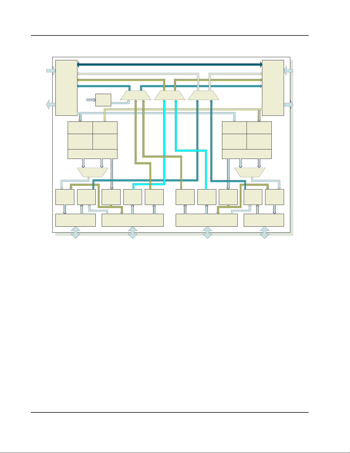
Figure 2: Block Diagram
2. Interface Operation30
Issue Path
2/4/8-bit HT
HyperTrans
port Link 0
Interface
Interrupt
Logic
Rx Cmd
Buffers
(24 Entries)
Rx Data RAM
(24 Entries)
Outbound
ReqCtl
(16 X 64)
(16 X 64)
PCI-X Master PCI-X Target
Data Mover
OutBound
ReqMux
PCI-X
Resp
Buffer
PCI-X Bus A
Rx Cmd
Buffers
(24 Entries)
Rx Data RAM
(24 Entries)
Outbound
(256 X 64)
(32 bit)
Accept Path
Data
RAM
Inbound
PReqMux
DelReqBuf
(4 Req
entries)
Forward Path
NPReq Mux
PReqBuf
RAM
(128 X 64)
Inbound
PReqBuf
RAM
(128 X 64)
Inbound
Resp Mux
DelReqBuf
(4 Req
entries)
PCI-X Target
Rx Cmd
Buffers
(24 Entries)
Rx Data RAM
(24 Entries)
Outbound
Data
RAM
(256 X 64)
PCI-X Bus B
(32 bit)
Issue Path
(24 Entries)
Rx Data RAM
(24 Entries)
Data Mover
OutBound
ReqMux
PCI-X
Resp
Buffer
(16 X 64)
HyperTrans
port Link1
Interface
Rx Cmd
Buffers
Outbound
(16 X 64)
PCI-X Master
2/4/8-bit HT
ReqCtl
Tsi308 User Manual
80D4000_MA001_02
Tundra Semiconductor Corporation
www.tundra.com
 Loading...