

TTI TG501 Service Manual

TG501
Function Generator
Service Manual
Book Part Number 48591-0130 - Issue 5

Table of Contents
General 1
Specification 2
Functional Description 4
Circuit Descriptions 6
Calibration 13
Parts List 17
General
Service Handling Precautions
Service work should only be carried out by skilled engineers. Please note that the tracks on the
printed circuit board are very fine and may lift if subjected to excessive heat. Use only a miniature
temperature controlled soldering iron and remove all solder with solder wick or suction before
attempting
to remove a component.
Dismantling the Instrument
WARNING!
Opening the instrument is likely to expose live parts. The instrument shall be disconnected from all
voltage sources before any adjustment, replacement or maintenance and repair during which it shall
be opened. If afterwards any adjustment, maintenance or repair of the opened instrument under
voltage is inevitable, it shall be carried out only by a skilled person who is aware of the hazards
involved.
1. Remove the 8 side screws and lift off the case upper and lower.
2. Access to all components is now possible, further dismantling is not necessary.
3. All small knobs are push on types. To remove the dial, remove the cap in the centre of the
knob using a knife blade, then loosen the nut about 1 turn. The knob and dial can then be
pulled off.
4. Transistors Q32, Q34 and Q39 and IC22 are insulated from the rear panel.
5. Reassemble in reverse order.
Operating Voltage
See the Power Supply section for details of changing the operating voltage from 220/240 to 110/120
and vice-versa.
1

Specification
(All specifications apply after warm-up in an ambient temperature range 18oC-28oC.)
OPERATING RANGE
Frequency Range: .005Hz to 5MHz in 7 overlapping decade ranges with fine
adjustmentby calibrated vernier.
Internal Mode
Vernier Range: 1000:1 within each range.
Vernier Accuracy: Better than ±5% of full scale.
External (Sweep) Mode:
Sweep Range: 1000:1 within each range.
FUNCTIONS
(Specifications apply for vernier between 0.5 and 5.0 and output 10V peak-to-peak into 50Ohm
termination).
Sine
Distortion: Less than 0.5% to 50kHz, less than 1% to 500kHz; all harmonics
>30dB below fundamental on 1M range.
Amplitude Flatness: ± 0.2dB to 500kHz; ±1dB to 5MHz.
Triangle
Linearity: Better than 99% to 500kHz.
Squarewave
Rise and Fall Times: <45ns.
Mark: Space Ratio: 1:1 ±1% to 100kHz; ± 5% to 5MHz
DC
Range: ±10V from 50 Ohm.
OPERATING MODES
Run
Generator runs continuously at the selected frequency.
Triggered
Generator is quiescent until triggered by an external input at TRIG IN or by pressing MANUAL. One
complete cycle is then generated at the selected frequency, starting and stopping at the phase set
by the START/STOP PHASE control.
Gated
Generator is quiescent until gated by an external signal at TRIG IN or by pressing MANUAL.
Generator then runs continuously at the selected frequency for duration of gate signal, starting and
stopping at the phase set by the START/STOP PHASE control. Last waveform started is
completed.
Manual
Manually operates generator as described in Triggered and Gated sections.
Start/Stop Phase
The START/STOP PHASE control varies the triggered and gated signal start/ stop point from
approximately -90o to +90o up to 500kHz.
2

Symmetry
When SYM is selected the SYMMETRY control varies the duty cycle from 1:19 to 19:1 to produce
sawtooth and variable pulse-width waveforms. The indicated frequency is divided by 10 with SYM
selected.
INPUTS
Sweep Input
Input Impedance: 10kOhm
Input Sensitivity: 0 to 4V for 1000:1 sweep
Maximum Allowable Input
Voltage:
±10V
Sweep Linearity: Better than 1%
Maximum Slew Rate of
Input Voltage:
0.1V/us
Trigger Input:
Frequency Range: DC - 5MHz.
Signal Range: TTL compatible levels; maximum input 20V.
Minimum Pulse Width: 50ns.
Input Impedance: Typically 2kOhm.
OUTPUTS
50 Ohm
Amplitude Control: >20dB vernier control within each attenuator range. Maximum output
20V peak-to-peak from 50Ohm (10V into 50Ohm).
Attenuator: Additional switch-selectable attenu- ation of 0, -20 or -40dB. Minimum
output <20mV peak-to-peak from 50Ohm (<10mV into 50Ohm).
DC Offset Control Range: ±10V from 50Ohm. DC offset plus signal peak limited to ±10V (±5V
into 50Ohm). DC offset plus waveform attenuated proportionally in 20dB and -40dB positions.
TTL
Amplitude: Fixed TTL level output at frequency and symmetry of main output.
Capable of driving 20 TTL loads.
GENERAL
Power Requirements
Input Voltage: 110/120V AC nominal 50/60Hz or 220/240V AC nominal 50/60Hz,
adjustable internally. The TG501 will operate safely and meet
specification within normal AC supply variations viz. 100-130V AC
and 200-260V AC respectively.
Power Consumption: 30VA Max.
Environmental Operating
Range:
+5oC to +40oC, 20% to 80% RH.
Storage Temperature Range:
-40oC to +70oC.
Size: 300mm wide x 100mm high x 230mm deep
Weight:
3.4kg
3

Functional Description
The relationships between the major circuit elements are shown in the block diagram opposite.
The summing amplifier sums the voltages from the dial and from the sweep input, and its output
controls the magnitude of the complementary current source and current sink. This current varies
from approximately 5.2uA to 5.2mA for a 1000:1 frequency change (.005-5.0).
The symmetry control adjusts the ratio between current source and current sink.
The diode gate steers current into or out of the range multiplier capacitor and is controlled by the
comparator output. When the comparator output is high the charge on the capacitor will rise,
linearly, producing the positive going triangle slope. When the comparator output is low the charge
on the capacitor will fall linearly producing the negative going triangle slope. The triangle amplifier
has unity gain and buffers the triangle wave on the multiplier capacitor to drive the comparator and
output circuits.
The comparator operates as a window detector with fixed limit points set to the triangle peaks. One
of its two outputs drives the TTL circuit and is also level shifted to drive the diode gate. The other
output drives the squarewave shaper. When the comparator output to the diode gate is high, the
triangle wave is positive going until this reaches approximately +1.2V, the comparator output then
switches low. When the comparator output is low the triangle wave is negative going until this
reaches approximately -1.2V, when the comparator output goes high, and the cycle is repeated.
4

This is the basic function generator loop in the Run mode and is shown by the double arrows in the
block diagram. Triangle and squarewave are generated simultaneously as shown.
The control logic determines Trig, Gate or Run modes. In Trig or Gate modes the waveform is
clamped by the -2I+ current sources and the diode gate, at a point determined by the Start/Stop
Phase control. A signal applied to Trig In releases the clamp and a single cycle is produced in the
Trig mode or a burst in the Gate mode, the waveform is then clamped again.
To achieve the 1, 10 and 100 ranges the 1k range capacitor is multiplied by 1000, 100 or 10 by the
capacitor multiplier circuit.
The TTL circuit buffers one of the comparator outputs to drive the TTL output socket.
The squarewave shaper converts the comparator output to a current signal and applies it to the
squarewave function switch. The sinewave converter uses the non-linear characteristics of a
transistor pair to convert the triangle wave into a sinewave, which is applied to the sinewave
function switch. The selected function is sent to the pre-amplifier where it is inverted and buffered
and applied to the output amplitude control. The signal is summed with the voltage from the DC
offset control at the output amplifier. This amplifier inverts and amplifies the signal up to 20V peak
to peak to drive the 50 Ohm output socket.
The power supply converts the incoming AC line voltage to the DC rails required by the instrument.
5
Circuit Descriptions
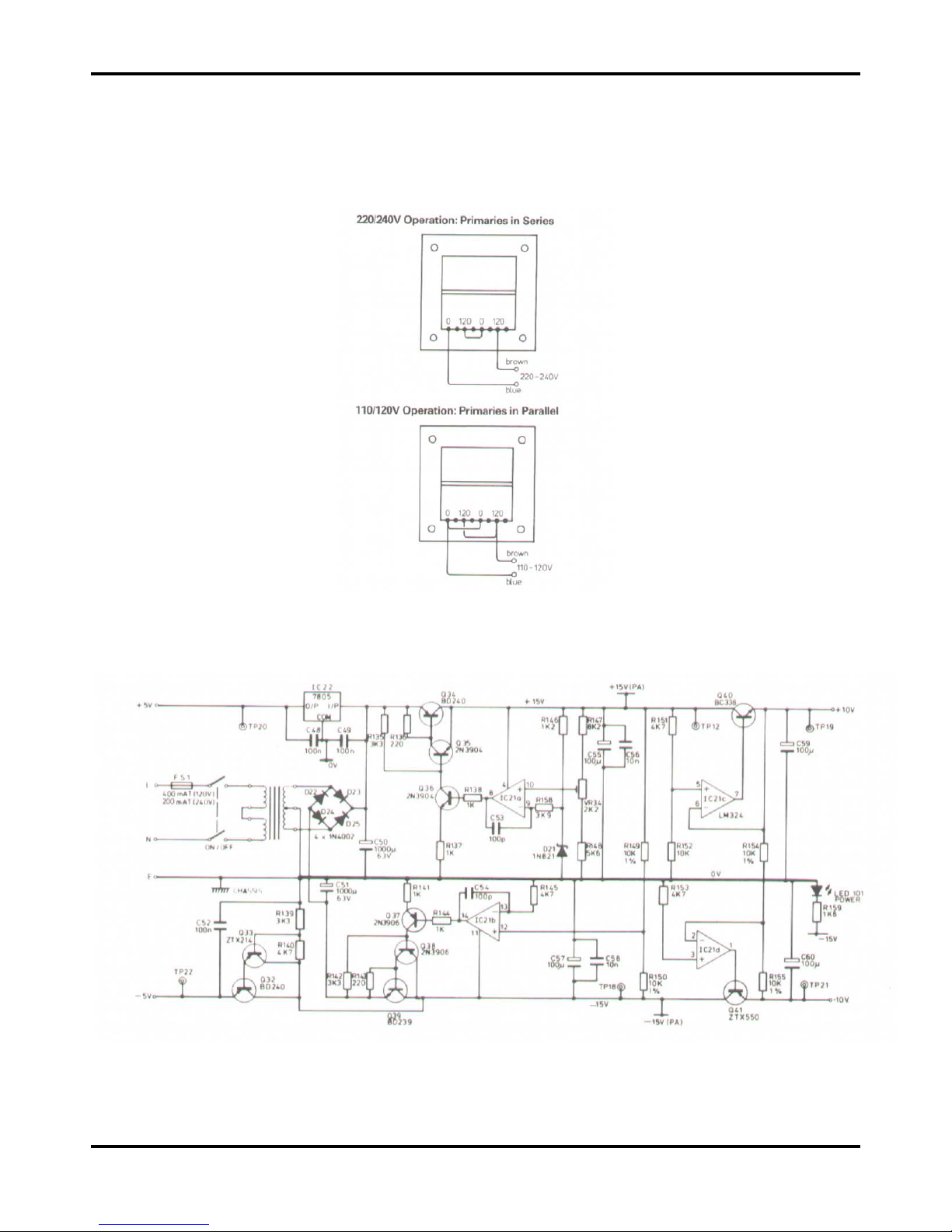
Power Supply - Mains connections
The operating voltage of the instrument is shown on the rear panel label. Should be it necessary to
change the operating range from 220/240V AC to 110/120V or vice-versa, change the transformer
connections following the appropriate diagram below.
If a change is made, the operating voltage label and fuse should also be changed.
For 220/240V operation use 200mA 250V time-lag
For 110/120V operation use 400mA 250V time-lag
WARNING! THIS INSTRUMENT MUST BE EARTHED
Any interruption of the protective conductor inside or outside the instrument or disconnection of the
protective earth terminal is likely to make the instrument dangerous. Intentional interruption is
prohibited.
6
Power Supply - DC Regulation
Diodes D22 to D25 rectify the transformer output and C50 and C51 are the reservoir capacitors of
the unregulated DC rails.
Q34, Q35, Q36 and IC21a form the +15V regulator, Q34 and Q35 form the compound series pass
element and Q36 its driver. IC21a is the error amplifier and a temperature compensated zener D21
provides the reference (6V2). The +15V output is set by VR34.
The -15V regulator is made up of Q37, Q38, Q39 and IC21b and complements the +15V regulator.
The -15V tracks the +15V by sensing the voltage at the junction of R149, R150 at the input of
IC21b.
The +10V rail is derived by dividing down the +15V rail; R151 and R152 provide the reference from
the +15V for the regulator IC21c and Q40.
The -10V regulator is formed by Q41 and IC21d and is the complement of the +10V regulator. The 10V tracks the +10V by sensing the voltage at the junction of R154,R155 at the input of IC21d.
The +5V rail uses a standard 3 terminal regulator IC22.
The -5V rail is divided down from the -15V by R139, R140 and buffered by a darlington emitter
follower Q32 and Q33.
Waveform Generation - Summing Amplifier and Current Sources
The dial and sweep voltages are summed by IC1, the gain of which is set by VR3. VR3 is, in fact,
used to calibrate the high end of the dial. The output range of the amplifier is approximately -4mV
(with the dial at .005) to -4V (with the dial at 5.0). This voltage is used to drive the complementary
current source and current sink as follows.
The emitter of Q1 is held at pseudo ground by IC2. If the dial is at 5.0, the -4V at the output of IC1
is forced at the emitter of Q2 by IC4. This -4V is also halved by R6, R7 and IC3 forces this voltage
(-2V) at the junction of R9, R10. A voltage dependant current is therefore set up through R8, R9,
R10 and R11.
IC5 is a current source controlled by the voltage on the collector of Q1 and IC6 is a current sink
controlled by the voltage on the collector of Q2. These two currents are steered into and out of the
range capacitor by the diode gate IC10, under the control of the comparator output.
7
When the symmetry button is depressed the short across VR8 is removed and the total resistance
between Q1 and Q2 emitters is increased from R to 10R. This lowers the current through this
resistor chain by a factor of 10 and so the frequency is divided by 10. Rotating VR8 imbalances the
current through Q1 and Q2 to give a duty cycle of up to 1:19 or 19:1.
With the symmetry button out, the waveform symmetry is set by VR9 at the top of dial (5.0). At the
bottom of the dail, symmetry is determined by offsets on ICs 1-6 (refer to calibration procedure).
Current source IC8 tracks the I+ current source IC5 and IC9 mirrors this to become -2I+. The -2I+
current is used to clamp the waveform in the Trig and Gate modes. The ramp can only stop in the
upward direction. When the Q output
of IC14b is set low, D1 is off. If the voltage at Q5 emitter is 0V (= to 0o), the voltage on the range
capacitor will ramp up and stop at 0V. When clamped the I+ current from the diode bridge flows
through the diode between pins 4 and 3 into the -2I+ current sink. A current equivalent to I+ also
flows through the diode between pins 9 and 1 into the -2I+ current sink to total 2I+. IC7 and Q5
buffer the voltage on the Start/Stop Phase control VR11 to give a low impedance voltage source on
pin 9 of IC10. This voltage can be varied between approximately +/-1.2V by VR11 corresponding to
the triangle peaks, giving +/-90o of phase control. To release the clamp the Q output of IC14b is set
high which pulls the -2I+ current sink high via D1, reverse biasing the two clamp diodes.
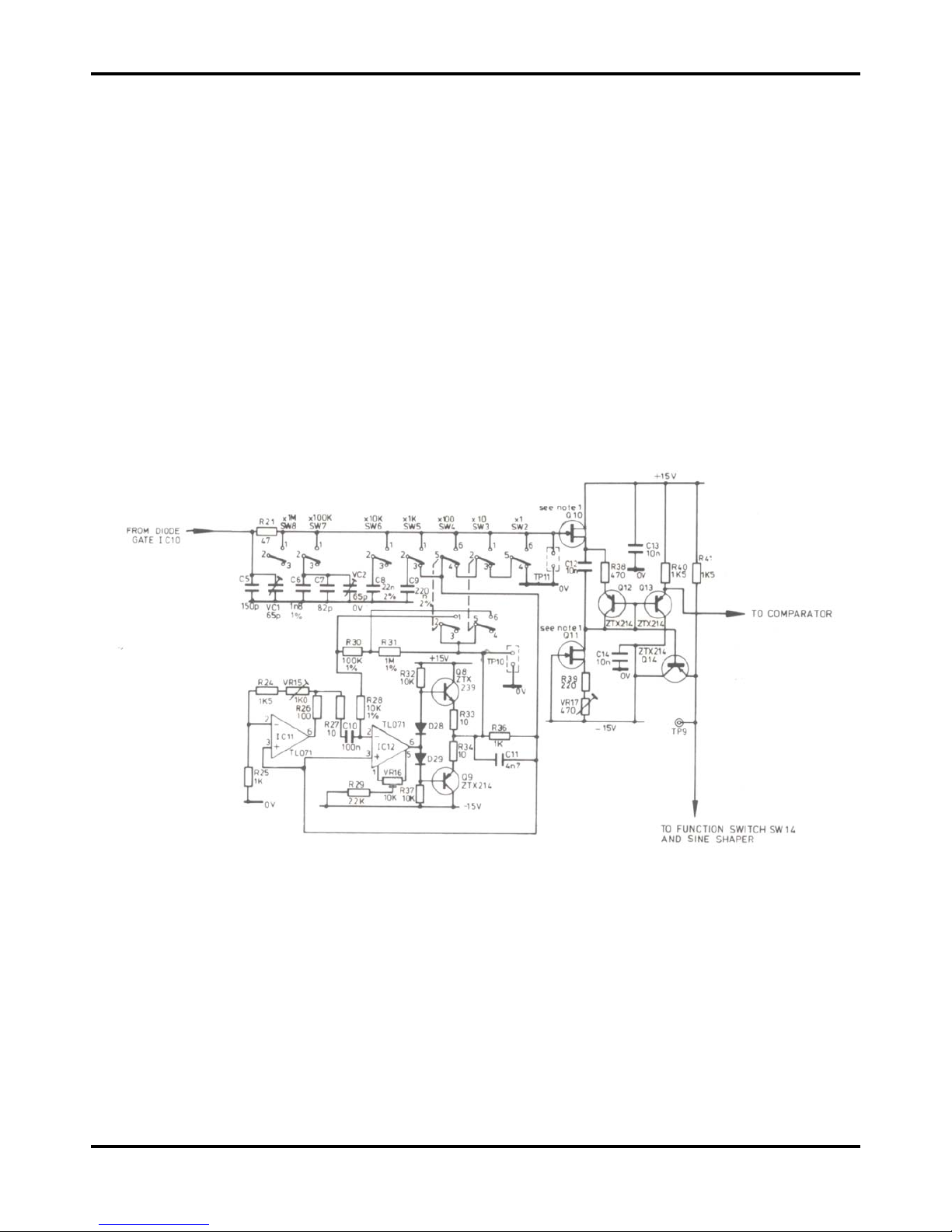
Waveform Generation - range selection and triangle amplifier
Range selection is by seven push-button switches, which steer the current sources into the
appropriate multiplier capacitor. The lower four ranges use the same range capacitor C9; the lower
three ranges use a capacitance multiplier. The capacitance multiplier steals current from the range
capacitor via R36. The amount of current taken is determined by the gain setting resistors R28,
R30 or R31 for the x100, x10 and x1 ranges respectively. The triangle wave on C9 is connected to
the non-inverting inputs of IC11 and IC12. The triangle wave is amplified by IC11 which has a gain
of 3; this is trimmed by VR15 to set the overall gain of the capacitance multiplier. Q8 and Q9 buffer
the output of IC12.
The triangle buffer consists of a FET source follower Q10 with temperature compensation provided
by current source Q11, which is I
DSS
matched with Q10. Q13 and Q14 are emitter followers to
provide 2 low impedance outputs. Q12 is strapped as a diode and compensates for the VBEs of
Q13 and Q14. VR17 trims the DC offset in this stage.
8

Waveform Generation - Comparator and TTL output
IC13 operates as a window detector and determines the peak to peak amplitude of the triangle
wave on the range multiplier capacitor, which is approximately +/-1.2V. C17-C22 compensate for
comparator and loop delays ensuring that the triangle wave amplitude remains constant with
increase in frequency. The two internal NAND gates in IC13 are wired as a flip-flop to ensure
positive switching of the comparator. C23 provides a small amount of positive feedback to ensure
jitter free operation. Some comparators oscillate with the dial at 0.005; this can be prevented by
fitting C66.
One of the comparator outputs is routed via IC17a to parallel gates IC17 c and d which drive the
TTL output. Q15 level shifts IC13 output to be about ground to drive the diode gates. Q16 is a VBE
multiplier and its total voltage is just under two VBEs. R45, R46 and C16 improve triangle linearity
at 5MHz.
IC15a and level shifter Q17 are used to drive the squarewave shaper circuit. When the squarewave
button is out, pin 4 of IC15a is held low and so the squarewave is gated off at the source.
9
 Loading...