

Page 1

SERVICE MANUAL
TCB-1100
MULTI CHANNEL AM/FM TRANSCEIVER
TTI Tech Co.,Ltd.
Downloaded from www.cbradio.nl
Page 2

TABLE OF CONTENTS
SECTION 1
SECTION 2
2-1
2-2
2-3
2-4
2-5
SECTION 3
SECTION 4
SECTION 5
5-1
5-2
5-3
5-4
5-5
5-6
SECTION 6
SECTION 7
SPECIFICATIONS
CIRCUIT DESCRIPTION
GENERAL
TECHNICAL DESCRIPTION
SEMICONDUCTORS AND FUNCTION
DESCRIPTION OF FREQUENCY DETERMINING AND STABILIZING CIRCUIT
TEST EQUIPMENT SETUP AND ALIGNMENT INSTRUCTIONS
PART LIST
MECHANICAL DISASSEMBLY
BOARD LAYOUT
MAIN PCB
LCD PCB
LED PCB
VOLUME PCB
SQUELCH PCB
CHANNEL PCB
BLOCK DIAGRAM
SCHEMATIC
Page 3
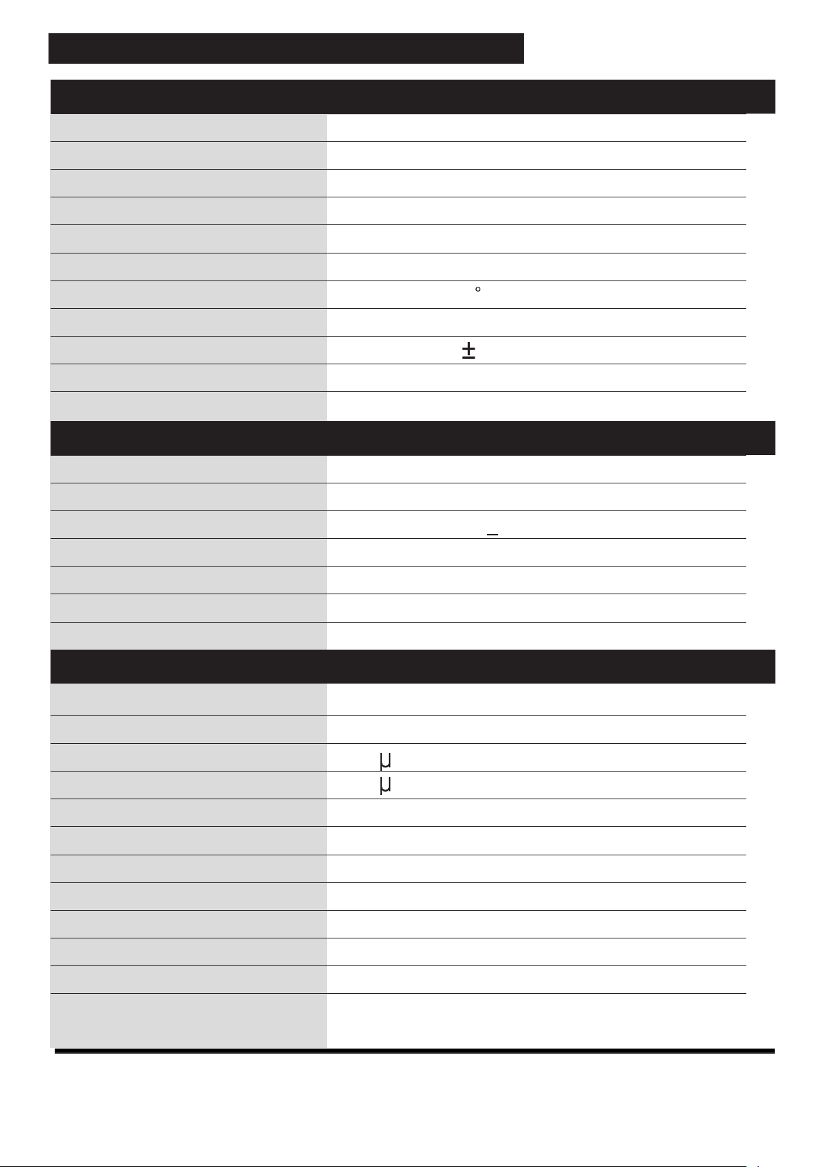
General
Channel
Frequency Range
Operating mode
Frequency Control
Frequency Tolerance
Operating Temperature
Range
Microphone
Input Voltage
Size
Weight
Power Output
Modulation
Frequency Response
Output Impedance
Harmonic Suppression
Current Drain
40 (See the frequency band
chart)
26.96 MHz ~ 27.99125 MHz
F3E (FM), A3E (AM)
PLL Synthesizer
0.002%
-10 to + 55 C
Plug-in Type
13.2V DC 15%
190(W) x 165(L) x 58(H)
978.5 g
Duty cycle 10% 4 Watts @13.8V
DC
AM:from 85% to 95%
FM:1.8KHz to +2.0KHz
300Hz to 3000Hz
50ohms, Unbalanced
Less than -36dBm
Receiving System
IF Frequencies
Sensitivity
Audio Output Power
Audio Distortion
Image Rejection
Adjacent Channel Rejection
Conducted Spurious
Frequency Response
Built-in Speaker
Transmitter
Receiver
Dual conversion superheterodyne
Double Conversion 1st 10.695MHz/2nd 455KHz
0.7 V for 10dB(S+N)/N in AM Mode
0.7 V for 20dB SINAD in FM Mode
2.0W @ 8 Ohm
Less then 8% @ 1KHz
60 dB
60 dB
Less than -57dBm
300 to 2500Hz
8 Ohms, round
Adjustable; Threshold less than 1 microvolt
DSS; Less than 2 microvolt
Transmitter
General
SECTION 1. SPECIFICATIONS
Page 4

SECTION 2. CIRCUIT DESCRIPTION
------------ Contents -------------
1 General
1-1.
Receiver
1.2. Transmitter
2.
Technical Description
2-1.
General
2-2.
Type of emission
2-3.
Frequency Table
2-4. RF Power Output
2-5. DC input Voltage and Current with 13.2V DC Input to Power AMP
2-6. Receiver IF and Local Oscillator Frequencies
3.
Semiconductors and Function
4.
Description of Frequency Determining and Stabilizing Circuit
4-1. Introduction
4-2. Basic Synthesis Scheme
4-3.
Descriptions of Each Block
4-3-1. Introductio
n
4-3-2.
Reference Frequency
4-3-3. VCO
4-3-4. Programmable Divider and Its Control
4-3-5 Phase Detector and VCO Control
4-3-6.
Transmitter / Receiver Buffer AMP
4-3-7.
Transmitter Buffer Amp
4-3-8. Switching of Turning Capacitor in VCO
4-3-9. Receiver Local Oscillator Outputs
4-4. Frequency Stability
4-5. Description of other Circuits
4-5-1.
Transmitter
4-5-2.
Receiver
5.
Test Equipment Setup and Test Procedure with Alignment Instructions
5-1. General Section.
5-1-2 Test Procedure with Alignment
5-2.
T ransmitter Section
5-2-2. Test Procedure and Alignment at TX
5-3. Receiver Section
5-3-2 Test Procedure and Alignment at RX
Page 5

TCB- 1100 Circuit Description Page 2
1. General
1-1. Receiver
① Display : 40 Channels and other functions indication
② Frequency Range : 26.965 to 27.405 [MHz]
③ Frequency Response : 300 to 2,500 [Hz]
④ Power Source : 13.2 [V] DC
⑤ Audio Output Load : 8 [OHM]
⑥ Audio Output : 4.0 [W] (or More)
⑦ Squelch : Adjustable from 0.2[uV] to 100 [uV]
⑧ Sensitivity :
- FM : 20 dB [SINAD] under 1.0 [uV] RF Signal or less
- AM :10 dB [S/N] under 1.0 [uV] RF Signal or less
⑨ Intermediate Frequency :
- 1st IF : 10.695 [MHz]
- 2nd IF : 455 [KHz]
1-2. Transmitter
① Carrier Power(Conducted)
② Current Drain ( 13.2 [V] Supply Voltage)
- No Modulation : 1,100 [mA]
- Max Modulation : 1
③ Modulation Capabilities
- AM : ± 90 [%]
- FM : ± 1.8 [KHz/Dev]
④ Spurious Radiation : Less then -54 [dBm]
⑤ Antenna Impedance : 50 [OHM]
⑥ Frequency Tolerance : 0.002 [%]
: AM 4 [W] / FM 4 [W]
,600 [mA]
TTI 2009-02-20
Page 6

TCB-1100 Circuit Description Page 3
2. Technical Description
2-1. General
2-2. Type of emission : AM(A3E) , FM(F3E)
Model TCB-1100 is an mobile type AM/FM radio transceiver for use of the Citizen Radio Service.
z Front Panel Controls
(1) LCD (Channel and RX/TX
(2) Receiver Audio Control Volume (With Power ON/OFF Control)
(3) Squelch Control Volume (With DSS ON/OFF Control)
(4) Channel UP/Down Rotary Switch
(5) CH9 Select Key / Menu Key
(6)
Scan Key / S.MEM Key
(7) DW Key / Vox Key
(8) Comp Key / Tone Key
(9) Back Light Select Key / Lock Key
(10) AM,FM Key / M Key
z Accessorily Connectors
(1) Antenna Socket
(2) External Speaker Jack (3.5mm)
(3) External S-meter Jack (2.5 mm)
(4) Microphone Connector (6 pin)
).
TTI 2009-02-20
Page 7
TCB-1100 Circuit Description Page 4
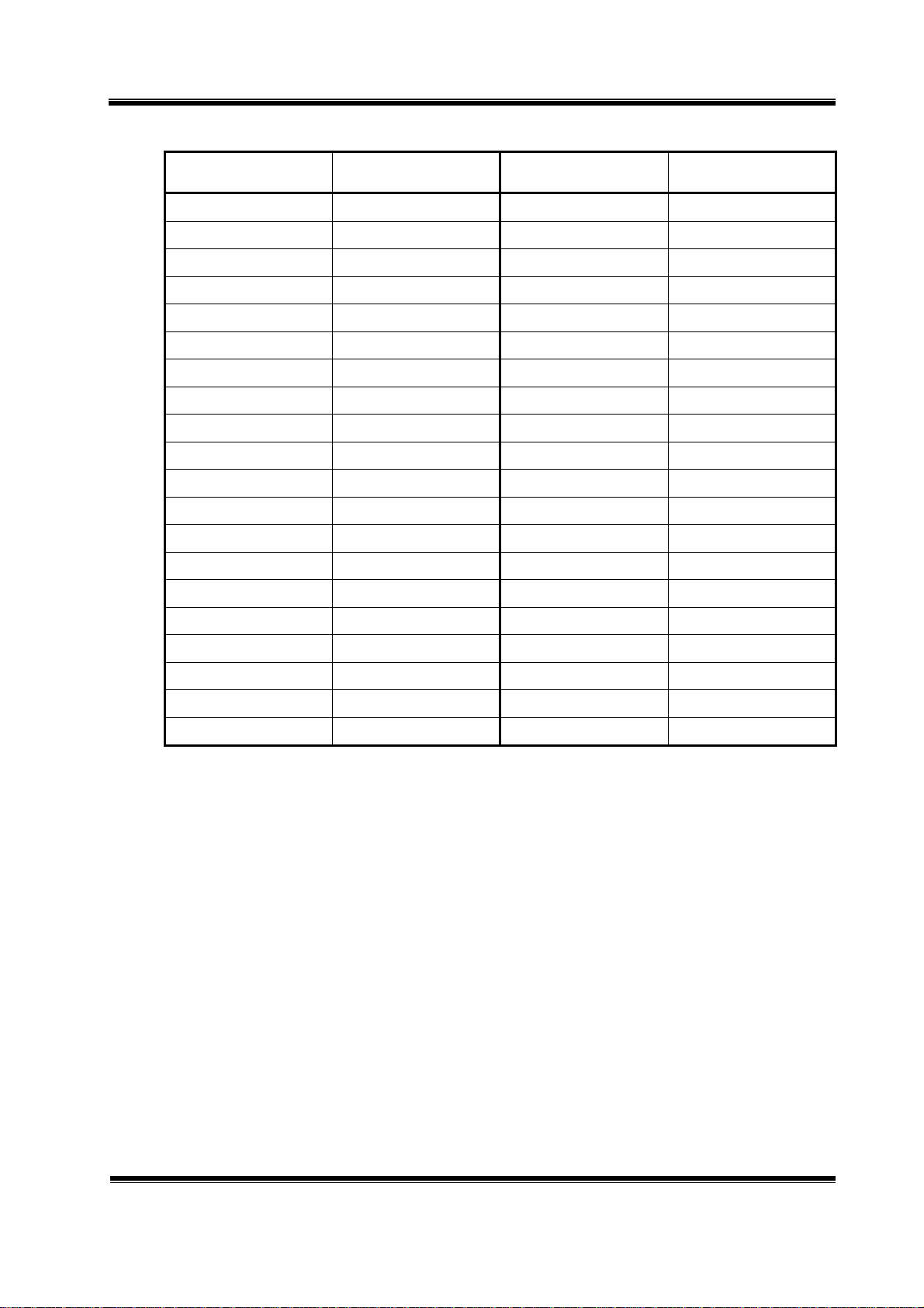
2-3. Frequency Table
Channel Frequency (MHz) Channel Frequency (MHz)
1 26.965 21 27.215
2 26.975 22 27.225
3 26.985 23 27.235
4 27.005 24 27.245
5 27.015 25 27.255
6 27.025 26 27.265
7 27.035 27 27.275
8 27.055 28 27.285
9 27.065 29 27.295
10 27.075 30 27.305
11 27.085 31 27.315
12 27.105 32 27.325
13 27.115 33 27.335
14 27.125 34 27.345
15 27.135 35 27.355
16 27.155 36 27.365
17 27.165 37 27.375
18 27.175 38 27.385
19 27.185 39 27.395
20 27.205 40 27.405
2-4. RF Power Output
z AM : 4.0 [W]
z FM : 4.0 [W]
2-5. DC Iinput Voltage and Current with 13.2V DC Input to Power AMP
z Transmitter Power Amp : Voltage 12.0 V
z Transmitter Driver Amp : Voltage 12.0 V
2-6. Receiver IF and Local Oscillator Frequencies
z First IF : 10.695 [MHz]
z Second IF : 455 [KHz]
z First Local Oscillator : 10.695 [MHz] Upper Receiving Frequency
z Second Local Oscillation : 10.240 [MHz]
Current 900 mA
Current 130 mA
TTI 2009-02-20
Page 8

TCB-1100 Circuit Description Page 5
3. Semiconductors and Function
3-1. Transistor
--------------------------------------------------------------------------------------------------------------------------------------------
Ref No. Description Manufacturer Function
--------------------------------------------------------------------------------------------------------------------------------------------
Q101 2SC4226 NEC RX Amplifier
Q102 KTK211 KEC 1’st Mixer
Q103 KTK211 KEC 1’st Mixer
Q107 KTC3875S KEC RX,RF/Mute,at-TX
Q108 KTC3875S KEC AGC
Q109 KTC3875S KEC AGC
Q110 KRC112S KEC S-Meter Dectector
Q112 KRC112S KEC FM AF Mute at AM Mode
Q118 KRC111S KEC RX AF Mute at TX Mode
Q114 KTC3880S KEC AM IF Amplifier
Q115 KTC3880S KEC AM IF Amplifier
Q113 KRA101S KEC RX AM(B+)switch
Q116 KTA1504S KEC Automatic Noise Level Control
Q111 KTC3875S KEC RX FM AF Amp
Q121 KTC1241 KEC TX,AM/1W-SW
Q132 KRC111S KEC TX,AM-AF,SW
Q201 KRC101S KEC AF Mute
Q117 KRC111S KEC AF Path
Q120 KTA1504S KEC Automatic Level Control
Q119 KTC3875S KEC Automatic Level Control
Q128 2SC4226 NEC VCO
Q129 KTC3880S KEC RX/TX VCO Buffer
Q130 KTC3880S KEC VCO Buffer
Q127 KRC101S KEC TX VCO Control
Q133 KRC111S KEC TX,Call Switching
Q125 KRC101S KEC TX Band2 Switching
Q155 KRC111S KEC TX,Mode Switching
Q146 KTC3875S KEC FM TX AF Mute at AM TX
Q134 KTC3880S KEC TX,Buffer
Q135 KTC3880S KEC TX Pre-Amplifier
Q136 2SC2314F SANYO TX Driver Amplifier
Q138 RD16HHF1 Mitsubishi TX Power Amplifier
Q153 KTA101S KEC TX SW
Q8 KRC404 KEC CPU Reset
Q152 KRC101S KEC RX/TX Control
Q154 KRA101S KEC TX,SW
Q122 KRC101S KEC FM,AM,Switch
Q154 KRA101S KEC TX,Switch
Q151 KRC111S KEC AM/FM,SW
Q145 KRC102S KEC Power Low Control
Q143 KTC3875S KEC 8.2V Regulator
Q142 KTC3875S KEC RX B+
Q141 KRA1504S KEC TX,B+
Q144 KTC3875S KEC
Q147 KRC111S KEC TX,Call-SW
5V.Regulator
TTI 2009-02-20
Page 9

TCB-1100 Circuit Description Page 6
Q1 KTA1505S KEC Back-Light,LED-Control
Q2 KRC101S KEC Back-Light,LED-Control
Q3 KRC101S KEC Back Light LED Control
Q4 KRC101S KEC Back Light LED Control
Q5 KRC110S KEC Back Light,LED Control
3-2. IC
--------------------------------------------------------------------------------------------------------------------------------------------
Ref No. Description Manufacturer Function
--------------------------------------------------------------------------------------------------------------------------------------------
IC1 SL5019 AUK IF IC
IC2 KIA358F KEC AGC, Squelch Control
IC3 TDA2003 ST AF Power Amplifier
IC4 LC7152NM SANYO PLL
IC5 KIA4558F KEC FM TX AF
IC8 CMX138 CML Tone.IC
IC10 4094B Rohm Shift,Resistor
IC11 KIA2576 KEC Switchlng,Power-Supply
IC12 H8/38124 Renesas CPU
IC13 AT24C16 ATMEL EEPROM
IC14 KIA324 KEC Auto-SQ,Amp(DSS)
3-3. Manufacture Information
z KEC ---------------------- KEC Co., LTD.
z SANYO ---------------------- SANYO Semiconductor Co., LTD.
z TOKO ---------------------- TOKO, Inc.
z TOSHIBA ---------------------- Toshiba Semiconductor. Co., LTD.
z ATMEL ----------------------
* NEC ----------------------- NEC Semiconductor
* AUK ----------------------- AUK Semiconductor
* Rohm ----------------------- Rohm Co.,Ltd
* Renesas ----------------------- Renesas Tech Nology Corp.
ATMEL Co., LTD
TTI 2009-02-20
Page 10
TCB-1100 Circuit Description Page 7
4. Description of Frequency Determining and Stabilizing Circuit
4-1. Introduction
The Frequencies for transmitter and receiver first local frequencies are all derived from a signal
4.5MHz crystal by means of a phase locked loop(PLL).
The first local oscillator frequencies are 37.660MHz(CH1) to 38.10MHz(CH40). The second local
frequency is fixed at 10.240MHz to generate second IF 455KHz.
Transmit, the VCO of the PLL operates 26.965MHz(CH1) to 27.405MHz(40CH). The VCO frequency
goes to the Buffer Amp circuit Q134, L701.
Q128
VCO
26.965MHz(CH1)
~
27.405MHz(CH40)
The VCO operating frequency for the receiver is 37.66MHz(CH1) to 38.10MHz(CH40) as the
first local oscillator, injected through the buffer amplifier Q129 into the first FET balanced mixer Q102,
Q103.
4-2. Basic Synthesis Scheme
The crystal frequency(4.5MHz) is divided by 1800 times to make 2.5KHz which is fed to one
side of the phase detector. The VCO output is divided by a programmable divider, and fed to other side of
the phase detector Pin 9, 10 of IC4. Passing the phase detector output closes the feedback loop through
an active low pass filter and using the output to control the VCO frequency through varicap diode D112.
Under locked conditions, both of phase detector input signal must be identical at 2.5KHz.
The VCO frequency is then given by ;
Receiver : Fvco / N = 0.005 [MHz] OR Fvco = 0.005 X N [MHz]
Transmitter : Fvco / N = 0.005 [MHz] OR Fvco = 0.005 X N [MHz]
Since “N” is an integer, the VCO frequency can be stepped up with in receiver mode 5KHz and
transmitter mode 5KHz increments.
By suitable choice of “N” the desired output frequency can be obtained.
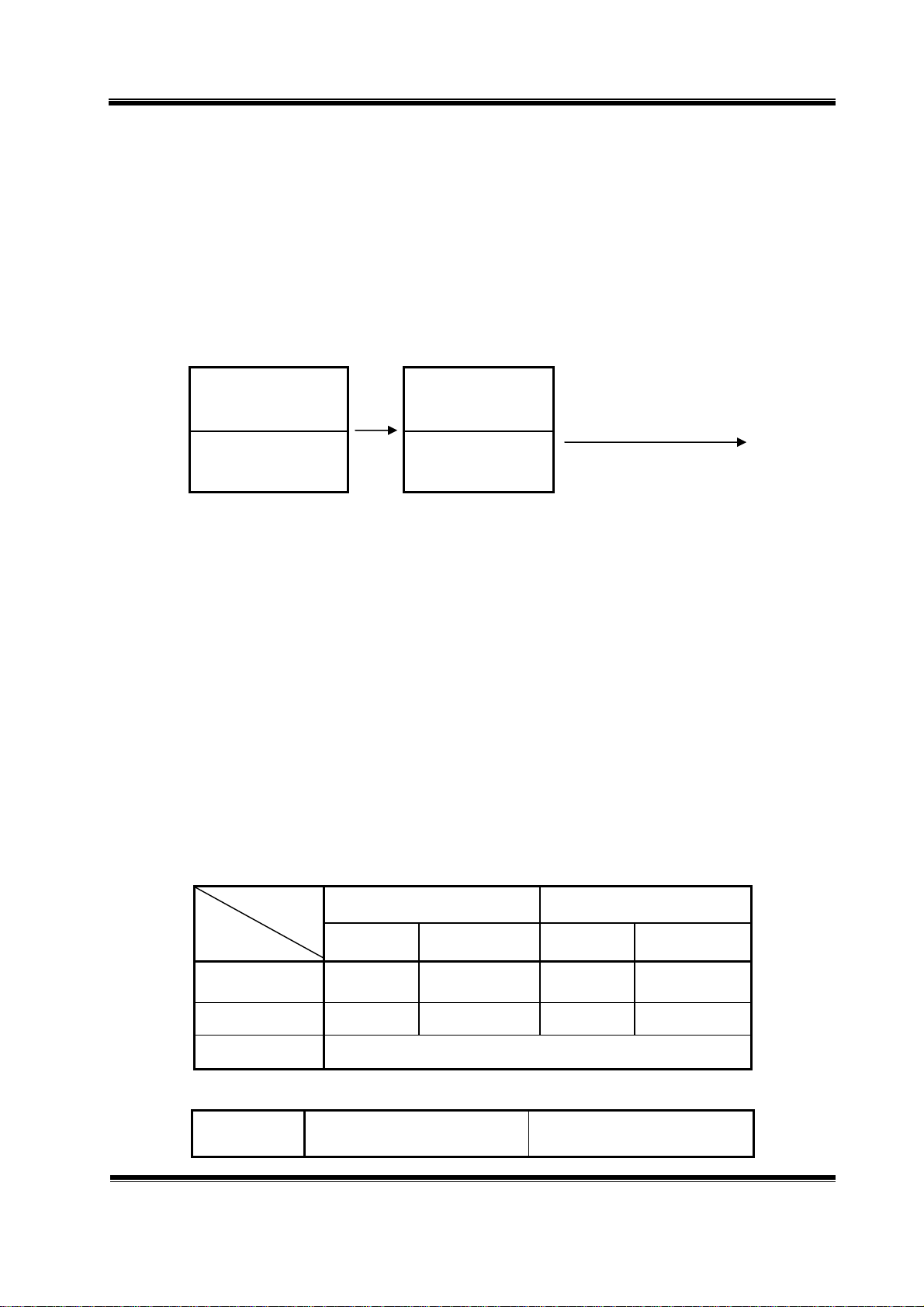
27.405MHz(CH40)
Q134
Buffer
26.965MHz(CH1)
To transmitter
~
Channel 1 Channel 40
N Fvco N Fvco
Transmit 5393 26.965 5481 27.405
Receiver 7532 37.660 7620 38.100
The VCO frequency goes to the Buffer Amp circuit,
VCO Output Frequency Buffer Output Frequency
TTI 2009-02-20
Page 11

TCB-1100 Circuit Description Page 8
Transmit
---
---
---
Transmit
Since all frequencies are obtained from the crystal controlled PLL oscillator, all outputs are
coherent with the crystal oscillator frequency and matching the sample percentage accuracy.
Note that the reference frequency of 5KHz, receiver and transmitter is obtained by
dividing the 4.5MHz by 900 times and 1800 times
CH 1 , 26.965 MHz
CH 40 , 27.405 MHz
26.965 MHz
27.405 MHz
TTI 2009-02-20
Page 12

TCB-1100 Circuit Description Page 9
4-3. Descriptions of Each Block
4-3-1. Introduction
The synthesizer is implemented with the following components;
PLL IC (IC4)
X-TAL (X102)
VCO, VARICAP DIODE (D112)
IC4 is CMOS LSI that includes most of PLL block.
The Q128, L301, C232, C242, C243, C244, varicap diode D112 are clap oscillator circuit to
operate as a VCO of the IC4. Q127 is a switching transistor to connect or disconnect the tuning
capacitor in the VCO oscillator tank circuit for transmitter or receiver.
Q129 works as a buffer amplifier for RX local frequencies (≒37MHz) and TX carrier
generating frequencies(≒26MHz)
4-3-2. Reference Frequency
The crystal X102(4.5MHz) and other components at Pin 1 and 24 of IC4 can make a reference
frequency oscillator with internal amplifier.
4-3-3. VCO
Q128 and surrounding parts are consisting a clap oscillator works as a VCO of IC4. With
appropriate control voltage on D112 the VCO can be oscillate over the required range of 26.965MHz to
38.10MHz.
4-3-4. Programmable Divider and Its Control
The programmable input for each channel are stetted by the PLL Clock(Pin 56), PLL Data(Pin
55), PLL Enable(Pin 58) of IC12. Each input signal to control the PLL ic is done with provide key input
Pin 73, 74, 75. For each key input, an internal code converts EEPROM
appropriate control to the programmable divider for that channel.
Since the change transmit and receive, and additional bit is required at Pin 66 of IC12 to allow
the ROM to recognize the status TX or RX.
During transmit the push to talk switch makes Pin 66 ground, PLL IC works
under transmit status.
The programmable divider output fed to the phase detector for compare with the 5KHz
reference frequency IC4. See table 1 for actual input and divide ratio on all channels.
4-3-5. Phase Detector and VCO Control
The phase detector is a digital phase comparator witch compares the phase of the reference
signal with programmable divider output square waves and develops a series of pulses whose dc level
depends on the phase error of each signal.
The phase detector pulse output is fed to an active low pass filter and RC low pass filter output
signal of IC4 is filtered and fed to varicap D112 control the VCO frequency.
4-3-6. Transmitter / Receiver Buffer AMP
Output signal of Q128 is fed into the buffer amplifier Q129, L3 to generate TX carrier
frequency and 1’st local frequencies.
TTI 2009-02-20
Page 13

TCB-1100 Circuit Description Page 10
4-3-7. Transmitter Buffer
The output signal of Q129, L3 goes to an amplifier with tuning circuit Q134, L701,
which buffer incoming 26MHz signals.
4-3-8. Switching of Turning Capacitor in VCO
The VCO circuit must tune with a wide range of frequencies 26.965MHz ~ 27.405MHz for
transmitter and 37.66MHz ~38.10MHz for receiver.
To comply above range of VCO, the tuning capacitance should switch for transmission. The
tuning circuit consists with L301, C232, C242, C243, and C244. When the VCO is working as a receiver
Q127 becomes turn OFF. So, L301 and C232, D112 makes turning function.
When transmitting, Q127 becomes ON. S the o, L301 an parallel capacitance of C232 and C241
make turning function.
4-3-9. Receiver Local Oscillator Outputs
z FIRST MIXER :
The secondary output signal of L107 is injected to the sources of 1’st mixer Q102, Q103 in the
1’st IF mixer section.
z SECOND MIXER :
The output of 10.24MHz oscillator circuit with X101 is injected into the IF IC(IC1) internally.
Incoming IF signal and 10.24MHz signal are mixed inside the IF IC to extract 2’nd IF signal 455KHz.
FM audio Signals are recovered with the way of quadrature detector.
AM signals are recovered with envelope detector.
4-4. Frequency Stability
Let : Fo = Crystal oscillator frequency
Fr = Phase detector reference frequency
Fvco = VCO frequency
Ft = Transmit frequency
Then : Receiver : Fr = Fo/900
Transmitter : Fr = Fo/900
And under locked conditions : Fr = Fvco / N
Where, “N” is the programmable divider divide ratio.
Then : Fvco = N X Fr)
From which it can be seen, the percentage error in Ft is the same as the percentage error in Fo.
The stability of the crystal oscillator is determined primarily by the crystal itself and having lesser
deviation by the active and passive components of the oscillator. The choice of crystal and components is
such that the required frequency stability is maintained over the required voltage and temperature range.
TTI 2009-02-20
Page 14

TCB-1100 Circuit Description Page 11
4-5. Description of other Circuits
4-5-1. Transmitter
A. RF Amplification
RF carrier frequencies are obtained at the output of buffer amplifier Q134 and turning IFT coil
L701, The input of VCO frequencies 26MHz is selected at the buffer output,
The output of buffer amplifier Q134 is fed through turning IFT coil L701, L703 to the base of pre driver
amplifier Q135. It’s output; 27MHz is coupled to RF driver amplifier Q136, a low-level class C power
amplifier. Driver Q136 supplies the necessary power gain to operate RF final Q138 at
the maximum efficient. The output of Q138 is supplied to the antenna through L-C turning circuit.
B. Circuit for Suppression of Spurious Radiation
The turning circuit between the output of final amplifier Q138 and antenna, 4-stage “π”
network C322, C323, C324, L711, C325, C326, L712, C328, C329, L713, C331, C332, C333, L714,
C334 serves as a spurious radiation suppressor. This network also servers to match the impedance
between TX power amplifier Q138 and the antenna.
C. Circuits for Limiting Power
After finished all alignment, the constant voltage supply circuit limits the available power 4W or
slightly less. RV106 and corresponding three-transistor control supply voltage of RF power amplifier.
When power low switch function Q145 changed the supply voltage. Tune all the trimming parts for
maximum indication of RF power meter and adjust RV104 to make 4W indication of RF power meter.
After finishing the above adjustments check the RF power meter reading is changed 1W under “LOW”
state.
The turning is adjustment so that the actual power is from 3.8W to 4.0W. There are no other
additional controls for adjusting the TX output power.
D. Modulation Control
Modulation of the RF is a process that begins with the audio picked up by the microphone.
<FM>
The microphone input is fed to mic audio amplifier IC5 that drives modulation vricap diode
D113 in the VCO circuit RV107 limits the incoming modulation audio levels to inhibit over modulation.
While reading the modulation factor on the modulation analyzing equipment, adjustment RV107 shall not
exceed 2.0KHz deviation.
<AM>
Modulation signals are filtered with RC network and goes to the audio power amplifier IC3 in
to make normal signal level to achieve wanted modulation. IC3 drives T101, which is a combination
AF output/modulation transformer. During transmit, one of the secondary windings of T101 is tied
between the 13.2V DC supply and the collectors of RF driver Q136 and RF power amplifier Q138. As the
audio passes through T101 it causes the collector supplies of Q136 and Q138 to vary with audio,
producing an AM signal at carrier frequency.
To avoid over modulation of the carrier, a protection of the modulating signal is fed back from
the T101 through the AMC circuit, Q119 and Q120, to control the gain of IC3 and sets the maximum
level of modulation. Form the center tab of RV102 and Q120 the feedback signal is rectified by diode
D109, filtered by C202, and supplied the Q119. The collector of Q119 is tied directly TX audio input to
control gain. That is, when the audio output is higher that the preset level of RV102, the information is
reflected through Q119 and Q120, reducing the gain of IC3
TTI 2009-02-20
Page 15

TCB-1100 Circuit Description Page 12
4-5-2. Receiver
Overload protection is provided to receiver’s semiconductors by diode D101. These diodes have
a little effect on the incoming signal from another CB station; they protect the receiver from stray
transmitter energy.
In the receiver mode of operation, Q142 transistor is turned on. Also bias voltage is applied to
Q101, Q102, Q103, IC1.
Q101 is a 27MHz RF input amplifier, and any excessive input signal is limited by diode D101.
CB receiver is dual conversion super-heterodyne type with the first IF 10.695MHz and the
second IF 455KHz.
Receiver is separated to blocks, 1’st IF section and 2’nd IF section. The PLL synthesizer
supplies 1’st local frequency 37.660MHz ~ 38.10MHz. The amplified 27MHz is mixed. With the
provide 1’st local frequencies Q102, Q103 mixes the incoming RF signal to generate 1’st IF signal. The
resulting first IF is 10.695MHz. Q102 and Q103 is the first converter, and 10.695MHz is sharply filtered
by L108 and crystal filter XF101. The first IF is again mixed with a second local oscillator of 10.24MHz.
With the 10.240MHz signal, IC1 FM IF IC converts the incoming signals to generate 2’nd IF
signal and recovered audio signals. 2’nd IF is filtered by a razor sharp ceramic filter CF101 coupled. The
455KHz signal from the 2’nd IF filter was amplified and limits internally. After amplification the signals
fed to the quardrature detector loop L109. Then could see the recovered signals Pin 8 of IC1.
With the amplitude of recovered signals, Q111 serves as an amplifier.
AM signals from the Pin 5 of IC1 were tapped with C135 and amplified two-stage amplifier
Q114, Q115. Q114 is a first 455KHz amplifier, and the Q114 being the last amplifier. D107 is a detector
diode witch produce audio signal as well as negative DC voltage for AGC action. The negative voltage
also provides forward biasing to the emitter of ANL clipping transistor Q116. The biasing voltage has a
time constant determined R162 and C168. Therefore any sharp negative going pulse from D107 will back
bias Q116 and clipped. The way to recover the AM information audio is envelope detector.
TTI 2009-02-20
Page 16

TCB-1100 Circuit Description Page 13
5. Test Equipment Setup and Test Procedure with Alignment Instructions
5-1 General Section
5-1-1 Test Equipment Required
• DC power supply(13.8V/3A)
• DC Voltmeter or Oscilloscope
• RF attenuator (30dB)
5-1-2 Test Procedure and Alignment
Step Setting Connection Adjuster Adjust for
1
RX VCO voltage Adj.
Channel & Frequency :
1CH, 26.956 MHz
Mic : Receive
Volume : Optional
Squelch : Optional
DC voltmeter to VCO
Test point (Figure 1)
L301 1.9~2.1 V DC
2
TX VCO voltage Adj.
Channel & Frequency :
1CH, 26.956 MHz
Mic : Transmit(No Mod)
Volume : Optional
Squelch : Optional
DC voltmeter to VCO
Test point (Figure 1)
Figure 1
L301 4.8~5.0 V DC
TTI 2009-02-20
Page 17

TCB-1100 Circuit Description Page 14
5-2 Transmitter Section
5-2-1 Test Equipment Required
• RF Power Meter • DC power supply(13.8V/3A)
• 50 ohms load (non-inductive) • Spectrum analyzer
• RF attenuator (30dB) • Frequency counter
• Oscilloscope • Coupler
• Audio generator • Modulation meter
5-2-2 Test Procedure and Alignment
Step Setting Connection Adjuster Adjust for
1
RF Power Adj.
Channel : 19CH
Function : AM or FM Mode
MIC : Transmit
Volume : Optional
Squelch : Optional
Connect dummy load and RF
Power Meter to the EXT–ANT
connector on the set(Figure 3)
L701
L703
Maximum
indication on
the Power
Meter(4.0W).
If indication is
not in 4W
range, ACP
Adjustment(R
V104)
2 Frequency Adj.
Channel & Frequency :
19CH, 27.185 MHz
Function : AM or FM Mode
Mic : Transmit(No Mod)
Volume : Optional
Squelch : Optional
3
AM Modulation Adj.
Channel & Frequency :
19CH, 27.185MHz
MIC: Transmit
Function : AM Mode
Volume : Optional
Squelch : Optional
Connect dummy load and
Frequency Counter through
Coupler to RF Power Meter.
Connect RF Power Meter to
EXT-ANT connector on the
set(Figure 2).
Connection the audio
generator (set to 1 KHz)to the
microphone.
Connect the modulation meter
through the RF attenuator to
the ANT Connector. Adjust
the audio signal level to obtain
by 50% modulation.
When you increase the audio
signal by 20 dB, the
modulation should not exceed
90% Modulation(Figure 3).
CT1 Be sure that
the indication
of the
transmitter
frequency is
27.185MHz
±300 Hz on
the Frequency
Counter
RV102 80% ~ 90%
TTI 2009-02-20
Page 18

TCB-1100 Circuit Description Page 15
4
FM Deviation Adj.
Channel & Frequency :
19CH, 27.185MHz
MIC : Transmit
Function : FM Mode
Volume : Optional
Squelch : Optional
Connection the audio
generator (set to 1 KHz)to the
microphone.
Connect the modulation meter
through the RF attenuator to
the ANT Connector. Adjust
the audio signal level to obtain
by 1KHz deviation.
When you increase the audio
signal by 20 dB, the deviation
should not exceed 2.0KHz
deviation(Figure 3).
RV107 1.8KHz ~
2.0KHz
Figure 3
Figure 2
TTI 2009-02-20
Page 19

TCB-1100 Circuit Description Page 16
5-3 Receiver Section
5-3-1 Test Equipment Required
• Standard Signal Generator(SSG)
• DC power supply(13.8V/3A)
• AC Level Meter
• Distortion Meter
• Oscilloscope
• SINAD Meter
• 8 ohm Dummy Load
5-3-2 Test Procedure with Alignment
Step Setting Connection Adjuster Adjust for
1
AM Audio Output Adj.
Channel & Frequency :
19CH, 27.185MHz
MIC : Receive
Function : AM Mode
Volume : Full clockwise
Squelch : Turn to counter
clockwise
Connect RF Signal Generator
to EXT-ANT Connector.
Connect AC Level Meter and
Distortion Meter and SINAD
Meter across EXT SPK jack
with 8 ohm Dummy
Load(Figure 4)
L101
L103
L104
L105
L107
L108
L110
Maximum
indication on
AC Level
Meter. Reduce
output from
SSG until the
audio output
becomes about
2V.
2
FM Audio Output Adj.
Channel & Frequency :
19CH, 27.185MHz
MIC : Receive
Function : FM Mode
Volume : Full clockwise
Squelch : Turn to counter
clockwise
3
Squelch Adj.
Channel & Frequency :
19CH, 27.185MHz
MIC : Receive
Function : FM Mode
SSG : 27.185MHz, 1KHz,
100uV, 1.2KHz Dev.
Volume : Full clockwise
Squelch : Full clockwise
clockwise
Connect RF Signal Generator
to EXT-ANT Connector.
Connect AC Level Meter and
Distortion Meter and SINAD
Meter across EXT SPK jack
with 8 ohm Dummy
Load(Figure 4)
Connect RF Signal Generator
to EXT-ANT Connector.
Connect AC Level Meter and
Distortion Meter and SINAD
Meter across EXT SPK jack
with 8 ohm Dummy
Load(Figure 5)
L109 Maximum
indication on
AC Level
Meter. Reduce
output from
SSG until the
audio output
becomes about
2V.
RV101 Adjust until
the audio
output
appears.
TTI 2009-02-20
Page 20

TCB-1100 Circuit Description Page 17
TTI 2009-02-20
Page 21

SECTION 3. PART LIST
NO PART NUMBER DESCRIPTION QTY VENDOR LOCATION NO.
1 5A0-1100-000 MAIN PCB ASS′Y - TCB1100 1.00
2 112-100J-S00 METAL OXID RESISTOR 10OHM 2W +-5 ST 1.00 R181
3 142-000J-000 CHIP RES. 0603 0OHM +-5 PHILIPS 2.00 R139A R119
4 142-100J-000 CHIP RES. 0603 10OHM +-5 PHILIPS 1.00 R222
5 142-101J-000 CHIP RES. 0603 100OHM +-5 PHILIPS 10.00
R104 R107 R143 R158 R159 R243 R305 R310 R179
R443
6 142-102J-000 CHIP RES. 0603 1KOHM +-5 PHILIPS 16.00
R121 R154 R170 R182 R202 R204 R205 R225 R226
R234 R236 R242 R313 R354 R434
7 142-103J-000 CHIP RES. 0603 10KOHM +-5 PHILIPS 25.00
R29 R42 R43 R114 R120 R133 R184 R194 R223
R237 R245 R248 R303 R402 R412 R416 R422 R423
R424 R426 R428 R429 R432 R435 R445
8 142-104J-000 CHIP RES. 0603 100KOHM +-5 PHILIPS 15.00
R100 R110 R122 R135 R141 R145 R169 R192 R241
R400 R411 R427 R430 R436 R438 R441
9 142-105J-000 CHIP RES. 0603 1MOHM +-5 PHILIPS 3.00 R186 R198 R408
10 142-123J-000 CHIP RES. 0603 12KOHM +-5 PHILIPS 1.00 R418
11 142-152J-000 CHIP RES. 0603 1.5KOHM +-5 PHILIPS 3.00 R125 R306 R352
12 142-153J-000 CHIP RES. 0603 15KOHM +-5 PHILIPS 3.00 R118 R156 R224
13 142-154J-000 CHIP RES. 0603 150KOHM +-5 PHILIPS 2.00 R185 R301
14 142-184J-000 CHIP RES. 0603 180KOHM +-5 PHILIPS 4.00 R405 R437 R439 R442
15 142-220J-000 CHIP RES. 0603 22OHM +-5 PHILIPS 1.00 R425
16 142-221J-000 CHIP RES. 0603 220OHM +-5 PHILIPS 3.00 R105 R106 R302
17 142-222J-000 CHIP RES. 0603 2.2KOHM +-5 PHILIPS 9.00 R171 R173 R206 R246 R249 R351 R356 R404 R453
18 142-223J-000 CHIP RES. 0603 22KOHM +-5 PHILIPS 14.00
R112 R131 R152 R153 R172 R201 R227 R229 R232
R247 R250 R300 R312 R406 R446 R447
19 142-224J-000 CHIP RES. 0603 220KOHM +-5 PHILIPS 4.00 R165 R199 R200 R395
20 142-225J-000 CHIP RES. 0603 2.2MOHM +-5 PHILIPS 2.00 R116 R363
21 142-229J-000 CHIP RES. 0603 2.2OHM +-5 PHILIPS 3.00 R175 R177 R178
22 142-272J-000 CHIP RES. 0603 2.7KOHM +-5 PHIILIPS 1.00 R157
23 142-273J-000 CHIP RES. 0603 27KOHM +-5 PHILIPS 2.00 R102 R407
24 142-302J-000 CHIP RES. 0603 3KOHM +-5 PHILIPS 2.00 R307 R308
25 142-333J-000 CHIP RES. 0603 33KOHM +-5 PHILIPS 2.00 R164 R417
26 142-334J-000 CHIP RES. 0603 330KOHM +-5 SAMSUNG_PHILIPS 1.00 R413
27 142-335J-000 CHIP RES. 0603 3.3MOHM +-5 PHILIPS 1.00 R139
28 142-391J-000 CHIP RES. 0603 390OHM +-5 PHILIPS 1.00 R362
29 142-470J-000 CHIP RES. 0603 47OHM +-5 PHILIPS 4.00 R132 R183 R309 R311
30 142-471J-000 CHIP RES. 0603 470OHM +-5 PHILIPS 4.00 R101 R108 R109 R134 R155 R203 R415
31 142-472J-000 CHIP RES. 0603 4.7KOHM +-5 PHILIPS 10.00 R111 R126 R176 R208 R304 R365 R401 R403 R433
32 142-473J-000 CHIP RES. 0603 47KOHM +-5 PHILIPS 14.00
R144 R151 R161 R162 R163 R193 R195 R196 R197
R221 R231 R409 R419 R421
33 142-474J-000 CHIP RES. 0603 470KOHM +-5 PHILIPS 6.00 R117 R142 R188 R189 R314 R364
34 142-563J-000 CHIP RES. 0603 56KOHM +-5 PHILIPS 5.00 R103 R136 R233 R235 R239
35 142-682J-000 CHIP RES. 0603 6.8KOHM +-5 PHILIPS 1.00 R115
36 142-683J-000 CHIP RES. 0603 68KOHM +-5 PHILIPS 1.00 R137
37 142-823J-000 CHIP RES. 0603 82KOHM +-5 PHILIPS 1.00 R166
38 142-824J-000 CHIP RES. 0603 820KOHM +-5 PHILIPS 2.00 R397 R414
39 162-102V-000 TRIM. POTENTIOMETER WS0612-B102-000-G36 CTR 1.00 CTR RV106
40 162-103V-000 TRIM. POTENTIOMETER WS0612-B103-000-G36 CTR 1.00 CTR RV101
41 162-104V-001 TRIM. POTENTIOMETER WS0612-B104-000-G36 CTR 3.00 CTR RV100 RV103 RV104
42 162-222V-001 TRIM. POTENTIOMETER WS0612-B222-000-G36 CTR 1.00 CTR RV102
43 162-223V-001 TRIM. POTENTIOMETER WS0612-B223-000-G36 CTR 1.00 CTR RV107
44 172-102J-000 NTC THERMISTOR 0603 1KOHM 18XQ102JOSRB MURATA 1.00 MURATA TH1
45 172-103J-800 NTC THERMISTOR 10KOHM NCP18XH103J03RB MURATA 1.00 MURATA TH2A
46 201-2272-M00 ELECT CAP. 220UF 10V 5x10 KOSHIN 1.00 KOSHIN C425
47 202-1059-M00 ELECT CAP. 1UF KR1-16V010MA 5x11 DONGXIANG 1.00 DON GXIANG C168
48 202-1065-M00 ELECT CAP. 10UF 16V 4x7 +-20 6.00 C147 C182 C203 C354 C372
49 202-1070-M01 ELECT CAP. 100UF 16V 5x11 KOSHIN 9.00 KOSHIN C120 C137 C250 C300 C352 C357 C377 C401 C432
50 202-1080-M00 ELECT CAP. 1000UF 16V 8x16 KOSHIN 5.00 KOSHIN C181 C184 C185 C359 C362
51 202-2249-M00 ELECT CAP. 0.22UF KR1-16VR22MA 5x11 DONGXIANG 1.00 DONGXIANG C138
52 202-4759-M00 ELECT CAP. 4.7UF KR1-16V4R7MA 5x11 DONGXIANG 1.00 DONGXIANG C255
53 202-4769-M00 ELECT CAP. 47UF KR1-16V470MA 5x11 DONGXIANG 4.00 DO NGXIANG C153 C202 C355 C415
Page 22

54 204-4770-M00 ELECT CAP. 470UF 35V 10x16 1.00 C363
55 212-010C-6C0 CHIP CERAMIC CAP. 0603 1PF NP0 50V +-0.25 PHILIPS 1.00 C341
56 212-030C-6C0 CHIP CERAMIC CAP. 0603 3PF NP0 50V +-0.25 PHILIPS 1.00 C251
57 212-050C-6C0 CHIP CERAMIC CAP. 0603 5PF NP0 50V +-0.25 PHILIPS 1.00 C127
58 212-080C-6C0 CHIP CERAMIC CAP. 0603 8PF NP0 50V +-0.25 PHILIPS 1.00 C247
59 212-101C-6J0 CHIP CERAMIC CAP. 0603 100PF NP0 50V +-5 PHILIPS 9 .00 C103 C115 C223 C224 C225 C243 C244 C307 C329
60 212-102B-3K0 CHIP CERAMIC CAP.0603 0.001UF X7R 16V +-10 PHILIPS 8.00 C102 C179 C186 C205 C229 C404 C428 C430
61 212-103B-3K0 CHIP CERAMIC CAP. 0603 0.01UF X7R 16V +-10 PHILIPS 32.00
62 212-104B-3K0 CHIP CERAMIC CAP.0603 0.1UF X7R 16V +-10 PHILIPS 36.00
C116 C121 C123 C124 C125 C126 C129 C135 C143
C152 C163 C171 C204 C234 C239 C245 C301 C302
C306 C351 C353 C356 C358 C364 C416 C417 C422
C110 C130 C133 C134 C136 C139 C142 C144 C151
C154 C155 C156 C162 C169 C206 C231 C235 C240
C248 C252 C342 C343 C402 C405 C407 C408 C410
C411 C412 C413 C414 C421 C424 C426 C427 C433
63 212-105F-3Z0 CHIP CERAMIC CAP. 0603 1UF Y5V 16V -20+80 PHILIPS 5.00 C119 C157 C161 C201 C237
64 212-121C-6J0 CHIP CERAMIC CAP. 0603 120PF NP0 50V +-5 PHILIPS 1 .00 C318
65 212-151C-6J0 CHIP CERAMIC CAP. 0603 150PF NP0 50V +-5 PHILIPS 5 .00 C104 C107 C111 C232 C322
66 212-180C-6J0 CHIP CERAMIC CAP. 0603 18PF NP0 50V +-5 PHILIPS 4.00 C108 C112 C128 C236
67 212-181C-6J0 CHIP CERAMIC CAP. 0603 180PF NP0 50V +-5 PHILIPS 2 .00 C254 C333
68 212-220C-6J0 CHIP CERAMIC CAP. 0603 22PF NP0 50V +-5 PHILIPS 2.00 C222 C242
69 212-221C-6J0 CHIP CERAMIC CAP. 0603 220PF NP0 50V +-5 PHILIPS 4 .00 C249 C309 C319 C332
70 212-223B-3K0 CHIP CERAMIC CAP. 0603 0.022UF X7R 16V +-10 PHILIP 5.00 C146 C167 C173 C178 C403
71 212-224B-3K0 CHIP CERAMIC CAP. 0603 0.22UF X7R 16V +-10 PHILIPS 4.00 C170 C175 C376 C379
72 212-273B-3K0 CHIP CERAMIC CAP.0603 0.027UF X7R 16V +-10 PHILIP 1.00 C439
73 212-331C-6J0 CHIP CERAMIC CAP. 0603 330PF NP0 50V +-5 PHILIPS 4 .00 C314 C315 C328 C373
74 212-390C-6J0 CHIP CERAMIC CAP. 0603 39PF NP0 50V +-5 PHILIPS 2.00 C114 C241
75 212-391C-6J0 CHIP CERAMIC CAP. 0603 390PF NP0 50V +-5 PHILIPS 3 .00 C323 C325 C326
76 212-470C-6J0 CHIP CERAMIC CAP. 0603 47PF NP0 50V +-5 PHILIPS 8.00 C101 C106 C109 C113 C132 C246 C253 C305
77 212-471C-6J0 CHIP CERAMIC CAP. 0603 470PF NP0 50V +-5 PHILIPS 4 .00 C100 C118 C313 C371
78 212-473B-3K0 CHIP CERAMIC CAP. 0603 0.047UF X7R 16V +-10 PHILIP 9.00 C141 C164 C165 C166 C226 C310 C311 C312 C321
79 212-474B-3K0 CHIP CERAMIC CAP. 0603 0.47UF X7R 16V +-10 PHILIPS 1.00 C183
80 212-560C-6J0 CHIP CERAMIC CAP. 0603 56PF NP0 50V +-5 PHILIPS 1.00 C131
81 212-680C-6J0 CHIP CERAMIC CAP. 0603 68PF NP0 50V +-5 PHILIPS 1.00 C105
82 212-681C-6J0 CHIP CERAMIC CAP. 0603 680PF NP0 50V +-5 PHILIPS 1 .00 C419
83 212-683B-6K0 CHIP CERAMIC CAP. 0603 0.068UF X7R 16V +-10 PHILIP 1.00 C418
84 212-820C-6J0 CHIP CERAMIC CAP. 0603 82PF NP0 50V +-5 PHILIPS 5.00 C304 C327 C331 C406 C409
85 212-821C-6J0 CHIP CERAMIC CAP. 0603 820PF NP0 50V +-5 PHILIPS 1 .00 C420
86 221-2243-M00 CHIP TANTAL CAP. 0.22UF 10V A SIZE +-20 1.00 C434
87 221-2254-M00 CHIP TANTAL CAP. 2.2UF 16V A SIZE +-20 1.00 C227
88 22D-101C-J00 DISK CAP. CC1HCH101J(100PF) 50V +-5 1.00 SAMIL C334
89 22D-470C-J00 DISK CAP. 47PF 50V +-5 1.00 C335
90 230-2000-000 DIP TRIMMER CAP. 6DIA 20PF KCVN620 FOKITS 1.00 FOKITS CT1
91 300-0211-000 CHIP TR. KTK211GR KEC 2.00 KEC Q102 Q103
92 300-1504-000 CHIP TR KTA1504S SOT-23 KEC 2.00 KEC Q116 Q120
93 300-1505-100 CHIP TR. SWITCHING (SOT-23) KTA1505S-Y KEC 1.00 KEC Q141
94 300-3875-000 CHIP TR. SWITCHING KTC3875S SOT-23 KEC 7.00 KEC Q107 Q108 Q109 Q111 Q119 Q142 Q144
95 300-3880-000 CHIP TR KTC3880S SOT-23 KEC 6.00 KEC Q114 Q115 Q129 Q130 Q134 Q135
96 301-4226-000 CHIP TR RF 2SC4226 R24 NEC 2.00 NEC Q101 Q128
97 302-1241-000 TRANSISTOR KTA1241 KEC 1.00 KEC Q121
98 302-2314-000 TR 2SC2314F SANYO 1.00 SANYO Q136
99 302-3205-000 TR. DIP TYPE KTC3205 KEC 1.00 KEC Q143
100 305-0101-000 CHIP TR KRC101S SOT-23 KEC 6.00 KEC Q113 Q122 Q125 Q127 Q152 Q154
101 305-0102-000 CHIP TR KRC102S SOT-23 KEC 1.00 KEC Q145
102 305-0110-000 CHIP TR KRC110S SOT-23 KEC 1.00 KEC Q131
103 305-0111-000 CHIP TR KRC111S SOT-23 KEC 7.00 KEC Q117 Q118 Q132 Q133 Q146 Q147 Q151
104 305-0112-000 CHIP TR KRC112S SOT-23 KEC 2.00 KEC Q110 Q112
105 305-9101-000 CHIP TR KRA101S SOT-23 KEC 1.00 KEC Q153
106 311-1610-000 POWER FET RD16HHF1 MITSUBISHI 1.00 MITSUBIS Q138
107 331-0324-A02 IC OP AMP KIA324F KEC 2.00 KEC IC 14 IC5
108 331-0358-A00 IC OP AMP KIA358F KEC 1.00 KEC IC2
109 332-2003-000 IC AUDIO AMP TDA2003 ST 1.00 ST IC3
110 333-2576-A00 IC REGULATOR KIA2576FP00(SMD TYPE) KEC 1.00 KEC IC11
111 335-7152-A00 IC PLL LC7152NM SANYO 1.00 SANYO IC4
112 336-5019-A00 IC IF SL5019 AUK 1.00 DAYTRONICS IC1
113 33C-0138-A00 IC CTCSS CMX138 CML 1.00 CML IC8
Page 23

114 33C-2576-A00 IC DD CONVERTER KIA2576PI00 KEC 1.00 KEC IC11
702-C1100
702-C1100
702-C1100
702-C7700
115 33C-4094-A00 IC BU4094BCFV ROHM 1.00 IC10
116 340-0230-A00 DIODE ZENER Z02W3.0V SOT-23 KEC 2.00 KEC D106 D122
117 340-0256-A00 DIODE ZENER Z02W5.6V SOT-23 KEC 1.00 KEC D118
118 340-0291-A00 DIODE ZENER Z02W9.1V SOT-23 KEC 1.00 KEC D119
119 341-0251-A00 DIODE VARICAP KDV251S SOT-23 KEC 4.00 KEC D100 D102 D112 D113
120 342-0033-A00 SCHOTTOKY DIODE SMAB33 KEC 1.00 KEC D120
121 342-0181-A00 CHIP DIODE SWITCHING KDS181 SOT-23 KEC 1.00 KEC D117
122 342-0184-A00 CHIP DIODE SWITCHING KDS184 SOT-23 KEC 5.00 KEC D24 D111 D114 D105 D115
123 342-0226-A00 CHIP DIODE SWITCHING KDS226 SOT-23 KEC 5.00 KEC D101 D110 D116 D123 D125
124 342-1114-A00 CHIP DIODE SWITCHING KDS114 KEC 1.00 KEC D104
125 343-1060-000 DIODE 1N60 2.00 D107 D109
126 343-4001-000 DIODE 1N4001 VISHAY 2.00 D108 D121
127 343-5402-000 DIODE 1N5402 1.00 D126
128 360-1024-001 CRYSTAL 10.24MHZ 32PF 30PPM HC-49U YOKETAN 1.00 YOKETAN X101
129 363-0045-000 CRYSTAL 4.5MHZ, HC-49S R49SDA-004500-FA-12-30-TA 1.00 YOKETAN X102
130 367-1060-200 CRYSTAL FILTER 10.695MHZ 49T-3L 10L08A DTRON 1.00 DTRON XF101
131 373-0455-100 CERAMIC FILTER LTM455HTW CQ 1.00 CQ CF101
132 400-0019-000 TRANSFORMER CHOCK T1 FINE 1.00 FINE T901
133 400-0028-000 TRANSFORMER EI-28(MOD) T2 FINE 1.00 FINE T101
134 406-0664-000 TROIDAL COIL 13X100UH 0.6X64T 1.00 FINE T902
135 406-2508-000 COIL SPRING 2.5X0.8X7T:R 0.11UH FINE 1.00 FINE L704
136 406-4005-000 COIL SPRING 4X0.5X6T:R FINE 2.00 FINE L712 L713
137 406-4005-300 COIL SPRING 4X0.5X9T : R FINE 1.00 FINE L714
138 406-5006-000 COIL SPRING 5X0.6X13.5T:R 0.5UH FINE 1.00 FINE L707
139 406-6008-000 COIL SPRING 6X0.8X5T:R 0.225UH FINE 1.00 FINE L711
140 410-0273-000 IFT COIL 27MHZ RX1(Wire Diameter : Φ0.1) FINE 1.00 FINE L101
141 410-0280-000 IFT COIL 28MHZ RX22 FINE 1.00 FINE L107
142 410-1070-000 IFT COIL 10.7MHZ RX-B RX3 FINE 1.00 FINE L108
143 410-1650-000 IFT COIL 16.5MHZ VCO VCO1 FINE 1.00 FINE L301
144 410-1651-000 IFT COIL 16.5MHZ VCO11 FINE 1.00 FINE L301
145 410-3011-000 IFT COIL TX 30MHZ TX11 FINE 1.00 FINE L701
146 410-3022-000 IFT COIL TX 30MHZ TX22 FINE 1.00 FINE L703
147 410-4550-000 IFT COIL DETECTOR 455KHZ RX4 FINE 1.00 FINE L109
148 410-4551-000 IFT COIL 455KHZ-B RX5 FINE 1.00 FINE L110
149 425-0150-000 COIL AXIAL 1.5UH AL0305 MATSUTA 2.00 MATSUTA L102 L106
150 425-1R00-001 COIL AXIAL 1UH AL0305 MATSUTA 1.00 MATSUTA L3
151 427-0010-000 COIL RF CHOKE 0.6x5.0x23.5TR 10uH 2.00 FINE L1 L2
152 427-0017-000 CORE SPRING 5.5TX0.45XM5ERX2.3 0.17UH FINE 3.00 FINE L103 L104 L105
153 427-0600-000 COIL CHOCK 6UH BOBBIN CORE 1.00 FINE L111
154 500-1100-000 MAIN PCB FR-4(2 LAYER 1.6T) 1.00 LUCKYVIEW
155 533-519V-000 SWITCH G5V-1 9V RELAY OMRON 2.00 ASUNG RE1 RE2
156 534-2505-000 SMD JACK SKJS-2513S-B SEKWANG 1.00 J201
157 534-3500-000 SMD JACK JY-3560-01-250 JT 1.00 JT J202
158 540-0218-000 WAFER 2PIN PH-2A 180C 1.00 FINE J205
159 540-0618-000 WAFER 6PIN PH-6A 180C 1.00 FINE J503
160 541-0239-002 CONNECTOR FD-ANT-1 NINGBO 1.00 NINGBO
161 547-0825-000 WIRE STRIP D0.8 L25MM 1.00 J701
162
163
164
165
166 5A0-1100-100 LCD PCB ASS′Y - TCB1100 1.00
167 142-000J-000 CHIP RES. 0603 0OHM +-5 PHILIPS 1.00 R23
168 142-102J-000 CHIP RES. 0603 1KOHM +-5 PHILIPS 3.00 R39 R40 R45
169 142-103J-000 CHIP RES. 0603 10KOHM +-5 PHILIPS 12.00 R5 R6 R7 R8 R10 R11 R12 R13 R22 R37 R44 R49
170 142-104J-000 CHIP RES. 0603 100KOHM +-5 PHILIPS 4.00 R1 R2 R3 R25
171 142-105J-000 CHIP RES. 0603 1MOHM +-5 PHILIPS 1.00 R47
172 142-123J-000 CHIP RES. 0603 12KOHM +-5 PHILIPS 1.00 R50
173 142-151J-000 CHIP RES. 0603 150OHM +-5 SAMSUNG_PHILIPS 1.00 R32
174 142-223J-000 CHIP RES. 0603 22KOHM +-5 PHILIPS 6.00 R4 R16 R18 R20 R21 R33
175 142-224J-000 CHIP RES. 0603 220KOHM +-5 PHILIPS 1.00 R24
176 142-331J-000 CHIP RES. 0603 330OHM +-5 SAMSUNG_PHILIPS 1.00 R35
TX TOP BRACKET SPTE 0.4T 1.00 DESHAN
TX BOTTOM PLATE SPTE 0.4T 1.00 DESHAN
TX BOTTOM BRACKET SPTE 0.4T 1.00 DESHAN
VCO SHIELD CAN SPTE 0.3T DESHAN 1.00 DESHAN
Page 24

177 142-471J-000 CHIP RES. 0603 470OHM +-5 PHILIPS 2.00 R31 R36
701-C1100
702-C1100
703-C1100
722-C0000
700-C110C
702-C1100
702-C1100
706-3008T
700-C110E
701-C1100
701-C1100
701-C1100
701-C1100
701-C1100
701-C7700
701-C88B0
703-C1100
706-2605S
715-C417N
719-S000D
700-C110M
178 142-472J-000 CHIP RES. 0603 4.7KOHM +-5 PHILIPS 1.00 R46
179 142-473J-000 CHIP RES. 0603 47KOHM +-5 PHILIPS 7.00 R9 R15 R17 R19 R26 R27 R28
180 142-681J-000 CHIP RES. 0603 680OHM +-5 PHILIPS 1.00 R38
181 142-682J-000 CHIP RES. 0603 6.8KOHM +-5 PHILIPS 1.00 R48
182 142-823J-000 CHIP RES. 0603 82KOHM +-5 PHILIPS 2.00 R30 R34
183 212-100C-6J0 CHIP CERAMIC CAP. 0603 10PF NP0 50V +-5 PHILIPS 1.00 C8
184 212-104B-3K0 CHIP CERAMIC CAP.0603 0.1UF X7R 16V +-10 PHILIPS 7.00 C1 C2 C3 C5 C7 C12 C14
185 212-220C-6J0 CHIP CERAMIC CAP. 0603 22PF NP0 50V +-5 PHILIPS 2.00 C9 C10
186 212-473B-3K0 CHIP CERAMIC CAP. 0603 0.047UF X7R 16V +-10 PHILIP 1.00 C11
187 221-106A-M00 CHIP TANTAL CAP. 10UF 6V A SIZE +-20 2.00 C4 C13
188 300-1505-100 CHIP TR. SWITCHING (SOT-23) KTA1505S-Y KEC 1.00 KECQ1
189 305-0101-000 CHIP TR KRC101S SOT-23 KEC 4.00 KEC Q2 Q3 Q4 Q5
190 305-0404-100 CHIP TR. KRC404 KEC 1.00 KEC Q8
191 322-3812-000 IC CPU (OTP) HD64F38124WV RENESAS 1.00 KOSHIDA IC12
192 338-2416-B00 IC EEPROM AT24C16N-10SI-2.7V ATMEL 1.00 ATMEL IC13
193 340-0230-A00 DIODE ZENER Z02W3.0V SOT-23 KEC 1.00 KEC D21
194 350-0036-000 LED DUAL(GREEN/AMBER) BL-HJCGK36J-TRB BRT LED 10.00 BRT LED D1 D2 D3 D4 D5 D6 D7 D8 D9 D10
195 350-0603-000 CHIP LED BLUE AOT-0603P-B01-V BLUEWIZ 10.00 D11 D12 D13 D14 D15 D16 D17 D18 D19 D20
196 352-4971-100 LCD SDM8A4971B SANTECH 1.00 SANTECH
197 363-3868-000 CRYSTAL 3.6864MHZ HC-49/S DTRON 1.00 DTRON X1
198 500-1100-100 LCD PCB FR-4(2 LAYER 1.6T) 1.00 LUCKYVIEW
199 500-1100-101 LCD BACKLIGHT PCB(L) 1.00 LUCKYVIEW
200 500-1100-102 LCD BACKLIGHT PCB(R) 1.00 LUCKYVIEW
201 539-0127-000 B TO B CONNECTOR F127-F-08DSG(SMD) FINE CONNECTOR 1.00 FINE CONNECTOR CON1
202 564-1109-100 SWITCH TACT KFC-821 GABOU 6.00 GABOU SW4 SW5 SW6 SW7 SW8 SW9
203
204
205
206
207 5A0-1100-200 VOLUME PCB ASS′Y - TCB1100 1.00
208 425-6R80-000 IND. AX 03TYPE LAL03TB6R8K(6.8UH) TAIYO YUDEN 1.00 L501 L502 L504 L506
209 500-1100-200 PCB VOLUME FR-4 (2 LAYER 1.0T) 1.00 LUCKYVIEW
210 540-0607-000 WIRE HARNESS PH-6PIN TO OPEN UL1007 NO.26 L=70mm 1.00 J502
211 541-0166-002 CONNECTOR SOCKET FD-MIC6PIN-F NINGBO 1.00 NINGBO J501
212 547-0415-000 HEAT SINK TUBE DIA4.0MM X 15MM 6.00
213 570-0901-001 VR R09710NS-KQ15A6.0-A103-015 CTR 1.00 CTR VR1
214 5A0-1100-300 SQUELCH PCB ASS′Y - TCB1100 1.00
215 500-1100-300 PCB SQUELCH FR-4 (2 LAYER 1.0T) 1.00 LUCKYVIEW
216 570-0902-001 VR R09710N0-KQ15A6.0-3B103-015 CTR 1.00 CTR VR2
217 5A0-1100-400 CHANNEL PCB ASS′Y - TCB1100 1.00
218 500-1100-400 PCB CHANNEL FR-4 (2 LAYER 1.0T) 1.00 LUCKYVIEW
219 560-9017-000 SW ROTARY TP90N17AE20 15SK TOCOS 1.00 TOCOS SW3
220
221 520-4500-000 SPEAKER 45PHI 4OHM 4W ACE 1.00 ACE
222
223
224
225
226
227
228
229
230
231
232
233
234
235 712-M70NI-001 RING NUT BsBm Ni PLATING 3.00 BONSO
236
237
238
239 543-1600-000 POWER CORD 2PIN PLUG ASS′Y UL1015#16 CABLE 1.00 BSQ
DIFFUSER ACRYL CLEAR 1.00 XINGTAI
LCD BRACKET SPTE 0.4T 1.00 DESHAN
ZEBRA SILICONE 38.2x7.91x1.0T 1.00 ATM
WHITE SHEET 64.20x23.20x0.1T 1.00 ATM
COVER ASS′Y - TCB1100 1.00
UPPER COVER SPC 0.8T BLACK UV COATING 1.00 DESHAN
BOTTOM COVER SPC 0.8T BLACK UV COATING 1.00 DESHAN
SCREW MACH(+) 3X8L-TAPTITE BLACK BH 8.00 BONSO FOR UPPER, BOTTOM COVER MOUNTING
ESCUTCHEON ASSY - TCB1100 1.00
ESCUTCHEON ABS BLACK 1.00 XINGTAI
WINDOW LENS ACRYL CLEAR 1.00 XINGTAI
ILLUMINATOR(VOL) ACRYL, CLEAR 1.00 XINGTAI
ILLUMINATOR(CH) ACRYL, CLEAR 1.00 XINGTAI
ILLUMINATOR(SQ) ACRYL, CLEAR 1.00 XINGTAI
CH KNOB ABS(BLACK COLOR) 1.00 SOLARIUM
SQ KNOB ABS BLACK SPRAY 2.00 SOLARIUM CH:1PCS , SQ:1PCS
KEYPAD SILICONE, NATURAL PU SOFT COATING 1.00 DAXIN
SCREW MACH(+) M2.6X5L Ni PLATED FH 4.00 BONSO FOR MAIN BODY+ESCUTCHEON MOUNTING
SPK FELT MESH BLACK Φ41.7x0.12T 1.00 BONSO
WINDOW TAPE 2X18X0.15T(3M ONESIDE DOUBLE TAPE) 2.00 ATM
MAIN BODY ASSY - TCB1100 1.00
Page 25

240
701-C4100
701-C5500
702-C1100
702-C1101
702-C7701
706-3008T
706-3010S
706-3010S
708-2608S
723-C4100
701-C5500
702-C1101
702-C7701
703-C7700
706-3008T
708-50121
701-C1100
701-C7701
701-C7701
701-C7701
701-C7701
701-C7701
703-C5500
241
242
243
244
245
246
247
248
CORD STOPPER PP BLACK 1.00 BONSO
BUSH NYLON66+GRASS 15% 1.00 SOARIUM
MAIN BODY EGI 1.0T 1.00 DESHAN
HEATSINK ALUMINUM 3.0t 1.00 DESHAN
ANT. TERMINAL SPTE 0.2T 1.00 DESHAN
SCREW MACH(+) 3X8L-TAPTITE BLACK BH 4.00 BONSO Main PCB + Main body mounting
SCREW MACH(+) M3X10L BLACK BH 2.00 BONSO TR MOUNTING
SCREW MACH(+) M3x10L Ni PLATED BH 2.00
SCREW Mach(+) M2.6x8L Ni plating BH 2.00 ATM MAIN BODY+LCD PCB MOUNTING
249 711-M30NI-000 NUT M3 Ni PLATED 4.00 BONSO TR MOUNTING
250 713-M30NI-S01 SPRING WASHER M3 4.00 BONSO TR MOUNTING
251
INSULATION WASHER PAPER Φ3.0 (Red color) 1.00 ATM
252 8A0-C110-000 PACKING ASS′Y - TCB1100 1.00
253 543-1600-100 POWER CORD 2PIN RECEPTACLE ASSY AWG16 10A BSQ 1.00 BSQ
254
255
256
257
258
259
STUD BOLT ABS M6X8L BLACK SOLARIUM 2.00 SOLARIUM
BRACKET SPC T=1.6 UV BLACK COATING 1.00 DESHAN
BRACKET MIC SUS304 1.0T 1.00 DESHAN
PACKING RUBBER 2.00 DAXIN
SCREW MACH(+) 3X8L-TAPTITE BLACK BH 2.00 BONSO
SCREW TAP(+) 5X12L-1S ZN PLATING TH 3.00 BONSO
260 714-M30NI-001 STAR WASHER-S M3 NI PLATING B TYPE 2.00 BONSO
261 714-M50NI-002 STAR WASHER-L M5 NI PLATING B TYPE 3.00 BONSO
262 801-C110-000 GIFTBOX SW1E 2.0T 1.00
263 804-C110-001 INNER BOX A SW1E 2.0T, WHITE 1.00
264 804-C110-002 INNER BOX B SW1E 2.0T, WHITE 1.00
265 809-C110-000 OUTBOX DW1E 7.0T 0.20
266 80A-C110-A00 OUTBOX PAD DW1E 7.0T 0.40
267 817-0520-000 POLYBAG PE 50X200 1.00
268 817-0810-000 POLYBAG PE 80X100 1.00
269 817-0832-000 Bracket POLYBAG PE 80x320mm 1.00
270 817-1090-000 POLYBAG PE 100X900X0.05T 1.00
271 817-2525-000 RADIO POLYBAG PE 250x250 1.00
272 820-C110-000 OWNER′S MANUAL 1.00
273 830-C110-000 Radio NAME LABEL 1.00
274 831-C110-000 AMC-5020 MIC NAME LABEL PE 22*12mm 1.00
275 833-C110-000 CODE 39 SERIAL NO. STICKER 2.00
276 834-0001-000 WARNING LABEL 1.00
277 834-0002-000 ROHS STICKER - TTI 0.20
278 834-C770-MC1 MIC LOGO STICKER PE 34.6*6.6*0.3T(REV.01) 1.00
279 834-CBCH-ST1 CB CHANNEL STICKER COPPER PAPER 100g/201X140mm 1.00
280 834-ROTE-R00 ROSTEST MARK STICKER 1.00
281 837-0001-000 OPP TAPE 50MM TTI LOGO 0.29
282 838-0001-000 YELLOW STRAP 0.26
283 83A-0001-000 SILICA GEL 1g 1.00
284 905-1100-000 MICROPHONE ASS′Y - TCB1100 1.00
285 100-273J-S00 FILM RES. 27KOHM 0.125W +-5 ST 1.00 ST R901
286 212-103B-3K0 CHIP CERAMIC CAP. 0603 0.01UF X7R 16V +-10 PHILIPS 1.00 C951
287 511-7700-000 PCB MIC 1.00 RICHO
288 523-9765-000 MIC CONDENSOR 4.5V 2.2K -44dB +-2dB 1.00
289 526-0051-001 CURL CORD 5CORD 1SHIELD FINE 1.00 FINE
290 541-0600-002 MIC CONNECTOR FD-MIC6PIN-M NINGBO 1.00
291 545-0280-000 LEAD WIRE BLK 3:3 65mm AWG28 1571 2.00
292 545-0281-000 LEAD WIRE RED 3:3 65mm AWG28 1571 2.00
293 545-0283-000 LEAD WIRE YELLOW 2:2 10mm AWG28 1571 1.00
294 562-2210-000 SW PUSH SKPS-2210C 1.00
295 564-1109-100 SWITCH TACT KFC-821 GABOU 3.00 GABOU
296
297
298
299
300
301
302
UPPER COVER ABS, BLACK UP/M/DOWN/SILK 1.00 SOARIUM
BOTTOM COVER ABS BLACK 1.00 SOARIUM
DECO ABS SILVER 1.00 SOARIUM
PUSH LEVER ABS BLACK 1.00 SOARIUM
KNOB ABS BLACK 3.00 SOARIUM
HOLDER PC BLACK 1.00 SOARIUM
SHRINKING TUBE BLACK(ID 6.0XOD7.0X6.0L) 1.00 BONSO
Page 26

303
703-C7700
703-C7700
708-26102
708-26162
718-R000D
718-R000N
723-C7700
304
305
306
307
308
309
310 817-1090-000 POLYBAG PE 100X900X0.05T 1.00 FOR MICROPHONE
311 831-C770-000 NAME LABEL PE 22X12X0.2T 1.00
312 834-C770-MC1 MIC LOGO STICKER PE 34.6*6.6*0.3T(REV.01) 1.00
SPK HOLDER RUBBER BLACK 1.00 LONGSHENDA
MIC BUSHING RUBBER BLACK 1.00 LONGSHENDA
SCREW TAP(+) 2.6X10L-2S BLACK FH 1.00 JLC
SCREW TAP(+) 2.6X16L-2S BLACK PH 4.00
CUSHION SPK20X24X8.0T(1SIDE DOUBLE TAPE)EVA SPONGE 1.00 BONSO
MIC SPONGE 30X7X3T (NO TAPE) EVA SPONGE BLACK 1.00 BONSO
SHRINGKAGE TUBE D3X50MM BLACK 1.00 BONSO
Page 27

SECTION 4. MECHANICAL DISASSEMBLY
Page 28

Page 29

SECTION 5. BOARD LAYOUT
5-1.Main PCB (Top Side)
Page 30

Main PCB (Bottom Side)
Page 31

5-2. LCD PCB (Top Side)
Page 32

LCD PCB (Bottom Side)
Page 33

5-3. LED PCB (Top Side)
Page 34

LED PCB (Bottom Side)
Page 35

5-4. Volume PCB (Top Side)
Page 36

Volume PCB (Bottom Side)
Page 37

5-5. Squelch PCB (Top Side)
Page 38

Squelch PCB (Bottom Side)
Page 39

5-6. Channel PCB (Top Side)
Page 40

Channel PCB (Bottom Side)
Page 41

SECTION 6. BLOCK DIAGRAM
Page 42

SECTION 7. SCHAMETIC
 Loading...