

Page 1

QL Series
Precision Power
Supplies
Service Manual
Book Part Number 48511-0670 - Issue 1
Page 2

Table of Contents
Specification 2
EMC 5
Safety 6
General 7
Circuit Descriptions 8
Calibration 11
Parts List 13
Block Diagram 31
Interconnection Diagram 32
Component Layouts 33
Circuit Diagrams 38
1
Page 3

Specification
General specifications apply for the temperature range 5°C to 40°C. Accuracy specifications
apply for the temperature range 18°C to 28°C after 1 hour warm-up with no load and calibration
at 23°C. Typical specifications are determined by design and are not guaranteed.
MAIN OUTPUTS
Voltage/Current Ranges:
QL355 QL564
0V to 35V/0·001A to 3A 0V to 56V/0·001A to 2A
0V to 35V/0·1mA to 500mA 0V to 56V/0·1mA to 500mA
0V to 15V/0·001A to 5A 0V to 25V/0·001A to 4A
Voltage Setting: Resolution 1mV
Accuracy ± (0·03% + 5mV)
Current Setting: Resolution 1mA; 0·1mA on 500mA range
Accuracy ± (0·2% + 5mA); ± (0·2% + 0·5mA) on 500mA range.
Output Mode: Constant voltage or constant current with automatic cross-over.
CI indicator lit in constant current mode.
Output Switch: Electronic, non isolating. Switch illuminated when Output on.
Preset voltage and current limit displayed when Output off.
Output Terminals: 4mm terminals on 19mm (0·75”) spacing for Output; screwless
terminals for Sense. Duplicate rear panel Output and Sense screw
terminals on remote control model (QL355P/TP & QL564P).
Transient Response:
<50µs to within 15mV of set level for a change in load current from full
load to half load or vice versa.
Voltage Programming
Speed:
Maximum time required for output to settle within 1% of its total
excursion (for resistive load). Excludes command processing time.
QL355 QL564
Full
Load
No
Load
Full
Load
No
Load
Up
Up
Up
15V 5A
35V 3A
35V 500mA
6ms
20ms
200ms
6ms
7ms
40ms
25V/4A
56V/2A
56V/500mA
10ms
40ms
300ms
6ms
15ms
60ms
Down
Down
Down
15V 5A
35V 3A
35V 500mA
6ms
25ms
120ms
250ms
600ms
600ms
25V/4A
56V/2A
56V/500mA
10ms
50ms
200ms
400ms
800ms
800ms
Ripple and Noise
(20MHz bandwidth):
Normal mode voltage: <0·35mVrms and 2mVp-p
Normal mode current: <0·2mArms; <20µArms on 500mA range.
Load Regulation:
For any load change, measured at the output terminals, using
remote sense.
Voltage <0·01% + 2mV.
Current <0·01% + 250µA; <0.01% +50µA on 500mA range.
Add typically 2·5mV for a 0·5V drop in the positive output lead.
Specification applies for sense lead resistance <0·5Ω.
Line Regulation: Voltage <0·01% + 2mV for 10% line change.
Current <0·01% + 250µA; <0.01%+ 50µA on 500mA range.
Temperature Coefficient: Voltage: typically <(50ppm + 0·5mV)/°C
Current: typically <(100ppm + 1mA)/°C;
(100ppm + 0·1mA)/°C on 500mA range.
Output Protection: Output will withstand forward voltages of up to 20V above rated output
voltage. Reverse protection by diode clamp for currents up to 3A.
2
Page 4

Over-voltage Protection:
(OVP)
Range 1V to 40V (QL355), 1V to 62V (QL564)
Resolution 0·1V; accuracy ± (2% + 0·5V)
Response time typically 100µs
Over-current Protection:
(OCP)
Range 0·01A to 5·5A (QL355), 0·01A to 4·4A (QL564)
Resolution 0·01A; accuracy ± (0·2% + 0·01A)
Response time typically 35ms
Protection Functions: Output trips off for OVP, OCP, over-temperature and Sense miswiring.
METER SPECIFICATIONS
Display Type: 5-digit (Volts), 4-digit (Amps), 14mm (0·56") LED.
Voltage (CI mode): Resolution 10mV
Accuracy ± (0·1% of reading + 10mV)
Current (CV mode): Resolution 0·001A; 0·1mA on 500mA range
Accuracy ± (0·2% + 0·005A); ± (0·2% + 0·5mA) on 500mA range
V x A: Resolution 0·01W; 0·001W on 500mA range
Accuracy ± (0·3% + 0·05W); ± (0·3% + 0·005W) on 500mA range
AUXILIARY OUTPUT (QL355T/TP)
Voltage: 2·7V, 3·3V or 5V, selectable by front panel switch.
Voltage Accuracy: ± 5%
Current Limit: 1A minimum
Output Protection: Output will withstand up to 16V forward voltage. Diode clamp reverse
protection for currents up to 3A.
Output Terminals: 4mm terminals on 19mm (0·75") spacing. Duplicate screwless
terminals on rear panel.
Ripple & Noise:
(20MHz bandwidth)
Typically <1mV rms
Load & Line Regulation: <1·0% for a 90% load change; 0·1% for a 10% line change.
Status Indication: Current limit lamp.
ALARM OUTPUT
Isolated rear-panel open-collector output signal. User can select output to be activated for either
OVP, OCP, Overtemperature or Sense miswiring, or for any of those four faults.
KEYBOARD & ROTARY CONTROL
All functions, including the selection and set-up of the remote control interfaces, can be set from
the keyboard. The rotary jog control can be used to adjust output voltage and current settings in
a quasi-analogue mode.
INTERFACES (QL355P/TP & QL564P only)
Full remote control facilities are available through the optional RS232, GPIB and USB interfaces.
Setting and readback resolutions are the same as for the Output and Meter specifications
respectively.
RS232: Variable Baud rate, 19200 Baud maximum. 9-pin D-connector.
Single instrument or Addressable RS232 Chain (ARC) operation.
IEEE-488: Conforming with IEEE488.1 and IEEE488.2
USB: Standard USB hardware connection.
Remote Command
Processing Time:
Typically <80ms between receiving the command terminator for a
step voltage change at the instrument and the output voltage
beginning to change.
3
Page 5

GENERAL
AC Input: 230V AC or 115V AC ± 10%, 50/60Hz. Installation Category II
Power Consumption: Single: 250VA max.
Triple: 500VA max.
Operating Range: +5ºC to +40ºC, 20% to 80% RH
Storage Range:
−40ºC to + 70ºC
Environmental: Indoor use at altitudes up to 2000m, Pollution Degree 2.
Cooling: Intelligent variable-speed fan.
Over-temperature trip shuts down output if internal temperatures
exceed predetermined thresholds.
Store/Recall: Up to 10 set-ups can be saved and recalled via the keyboard or remote
interfaces.
Safety:
Complies with EN61010−1
EMC: Complies with EN61326
Size: Single: 140 x 160 x 290mm (WxHxD), excluding feet and terminals.
Triple: 280 x 160 x 290mm (WxHxD), excluding feet and terminals.
Weight: Single: 5·5kg
Triple: 10·5kg
4
Page 6

EMC
This instrument has been designed to meet the requirements of the EMC Directive 89/336/EEC.
Compliance was demonstrated by meeting the test limits of the following standards:
Emissions
EN61326 (1998) EMC product standard for Electrical Equipment for Measurement, Control and
Laboratory Use. Test limits used were:
a) Radiated: Class B
b) Conducted: Class B
c) Harmonics: EN61000-3-2 (2000) Class A; the instrument is Class A by product category.
Immunity
EN61326 (1998) EMC product standard for Electrical Equipment for Measurement, Control and
Laboratory Use.
Test methods, limits and performance achieved were:
a) EN61000-4-2 (1995) Electrostatic Discharge : 4kV air, 4kV contact, Performance A.
b) EN61000-4-3 (1997) Electromagnetic Field, 3V/m, 80% AM at 1kHz, Performance A.
c) EN61000-4-11 (1994) Voltage Interrupt, 1 cycle, 100%, Performance B.
d) EN61000-4-4 (1995) Fast Transient, 1kV peak (AC line), 0·5kV peak (DC Outputs),
Performance B.
e) EN61000-4-5 (1995) Surge, 0·5kV (line to line), 1kV (line to ground), Performance B.
f) EN61000-4-6 (1996) Conducted RF, 3V, 80% AM at 1kHz (AC line only; DC Output
connections <3m not tested), Performance A.
According to EN61326 the definitions of performance criteria are:
Performance criterion A: ‘During test normal performance within the specification limits.’
Performance criterion B: ‘During test, temporary degradation, or loss of function or
performance which is self-recovering’.
Performance criterion C: ‘During test, temporary degradation, or loss of function or
performance which requires operator intervention or system reset occurs.’
Where Performance B is stated it is because DC Output regulation may deviate beyond
Specification limits under the test conditions. However, the possible deviations are still small and
unlikely to be a problem in practice.
Note that if operation in a high RF field is unavoidable it is good practice to connect the PSU to
the target system using screened leads which have been passed (together) through an absorbing
ferrite sleeve fitted close to the PSU terminals.
Cautions
To ensure continued compliance with the EMC directive observe the following precautions:
a) after opening the case for any reason ensure that all signal and ground connections are
remade correctly and that case screws are correctly refitted and tightened.
b) In the event of part replacement becoming necessary, only use components of an
identical type, see the Service Manual.
5
Page 7

Safety
This power supply is a Safety Class I instrument according to IEC classification and has been
designed to meet the requirements of EN61010-1 (Safety Requirements for Electrical Equipment
for Measurement, Control and Laboratory Use). It is an Installation Category II instrument
intended for operation from a normal single phase supply.
This instrument has been tested in accordance with EN61010-1 and has been supplied in a safe
condition. This instruction manual contains some information and warnings which have to be
followed by the user to ensure safe operation and to retain the instrument in a safe condition.
This instrument has been designed for indoor use in a Pollution Degree 2 environment in the
temperature range 5°C to 40°C, 20% - 80% RH (non-condensing). It may occasionally be
subjected to temperatures between +5°C and –10°C without degradation of its safety. Do not
operate while condensation is present.
Use of this instrument in a manner not specified by these instructions may impair the safety
protection provided. Do not operate the instrument outside its rated supply voltages or
environmental range.
WARNING! THIS INSTRUMENT MUST BE EARTHED
Any interruption of the mains earth conductor inside or outside the instrument will make the
instrument dangerous. Intentional interruption is prohibited. The protective action must not be
negated by the use of an extension cord without a protective conductor.
When the instrument is connected to its supply, terminals may be live and opening the covers or
removal of parts (except those to which access can be gained by hand) is likely to expose live
parts. The apparatus shall be disconnected from all voltage sources before it is opened for any
adjustment, replacement, maintenance or repair.
Capacitors inside the power supply may still be charged even if the power supply has been
disconnected from all voltage sources but will be safely discharged about 10 minutes after
switching off power.
Any adjustment, maintenance and repair of the opened instrument under voltage shall be avoided
as far as possible and, if inevitable, shall be carried out only by a skilled person who is aware of
the hazard involved.
If the instrument is clearly defective, has been subject to mechanical damage, excessive moisture
or chemical corrosion the safety protection may be impaired and the apparatus should be
withdrawn from use and returned for checking and repair.
Make sure that only fuses with the required rated current and of the specified type are used for
replacement. The use of makeshift fuses and the short-circuiting of fuse holders is prohibited.
Do not wet the instrument when cleaning it.
The following symbols are used on the instrument and in this manual:-
Earth (ground) terminal.
mains supply OFF.
l
mains supply ON.
alternating current (ac)
direct current (dc)
6
Page 8

General
Service Handling Precautions
Service work or calibration should only be carried out by skilled engineers using high quality test
equipment. If the user is in any doubt as to his competence to carry out the work, the instrument
should be returned to the manufacturer or their agent overseas for the work to be carried out.
Please note the following points before commencing work.
The tracks on the printed circuit boards are very fine and may lift if subjected to excessive heat.
Most of the integrated circuits are static sensitive and great care should be taken when handling
them to avoid damage due to static discharge. Also, most devices on the Control board are
surface mounted components with very fine leads on small pitches. These components must be
removed and replaced with great care to avoid damage to the PCB. It is essential that only the
proper tools and soldering equipment as recommended for surface mount components are used.
Dismantling the instrument
WARNING!
Disconnect the instrument from all voltage sources before it is opened for adjustment or repair. If
any adjustment or repair of the opened instrument is inevitable it shall be carried out only by a
skilled person who is aware of the hazards involved.
1. Remove the six screws retaining the top cover and lift clear.
2. To remove the pcbs, first improve access by unscrewing the front panel: remove the screw(s)
securing the front panel bracket(s) to the spacer in the centre of the Power pcb(s) and remove
the screws that fix the bottom edge of the front panel to the chassis. The front panel can be
tipped forward to give access to the latching connectors connecting the Keyboard to the Power
pcb; disconnect these, noting orientation.
3. To remove the Power and Control pcbs remove the two screws securing the Power pcb to the
central fan bracket and the two screws fixing the Power pcb bracket to the rear panel. Unplug the
two transformer connectors, the fan connector and any inter-pcb connections (Power to Power on
a triple output supply, and/or Power to Interface on programmable versions) noting their positions
carefully; a diagram is provided at the end of this manual showing how these connections are
made. The Control pcb is plugged into the Power pcb and both can now be lifted clear together.
4. The Display/Keyboard pcb can be removed from the front moulding after pulling off the jog wheel
and removing the fixing screws, two of which also secure the front panel bracket (four on the
triple).
5. To remove the Interface pcb from the rear panel, undo the jackscrews of the GPIB and RS232
sockets and the self-tap screw in the chassis which retains the inner support bracket.
6. When re-assembling the instrument ensure that all fixings use the correct fasteners. Replace cut
cable ties. Do not over tighten the display/keyboard fixing screws in the moulding. Check that the
fan operates.
7
Page 9

Circuit Descriptions
The Power board contains the main power supply and the auxiliary supplies used internally, the
output series regulator transistors, the microcontroller, display drivers and some control logic.
The Control board contains voltage and current control, ADC and DAC and some control logic.
The linear regulator is in series with the positive output but, because of the way in which the
control circuit is referenced to the +ve output, it is convenient to consider the regulated output as
the negative side.
To help reading the circuit diagrams the two connectors between the power and control pcbs join
as follows. PJ14 to PJ18 and PJ20 to PJ19.
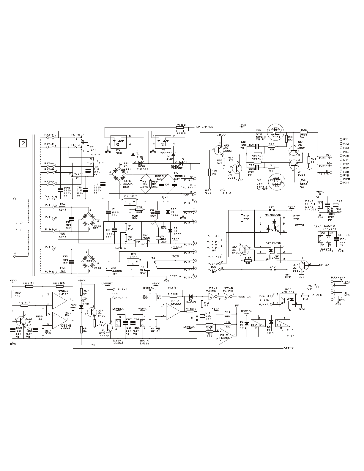
Power Pcb
The main windings are connected either in series (for the high voltage range) or in parallel (for
the low voltage range) by the range relays and an electronic tap change at approximately half
range is used to reduce dissipation. Bridge rectifier BR1 feeds C4 the reservoir capacitor when
tap change is low. When tap change is high, two of the diodes in BR1 are bypassed by SCR1 and
SCR2. Voltages are listed below at nominal mains (230V).
QL355
35V/3A 15V/5A
Secondary – high tap, no-load 39.8VAC 19.9VAC
Secondary – high tap, full-load 37VAC 18.9VAC
C4 – high tap, no-load 51.5VDC 24.5VDC
C4 – high tap, full-load 44.7VDC 21.9VDC
QL564
56V/2A 25V/4A
Secondary – high tap, no-load 60VAC 30.1VAC
Secondary – high tap, full-load 56VAC 28.6VAC
C4 – high tap, no-load 79.5VDC 38.4VDC
C4 – high tap, full-load 69.5VDC 35.2VDC
A 30Vrms centre tapped winding and full wave rectification provide the auxiliary supplies. IC1
generates +10V and IC2 –5V. A 10.4Vrms winding and full wave rectification power the relays
and fan and IC3 provides the +5V for the microcontroller, display and control logic.
Comparator IC6A provides the system reset signal and comparator IC6B provides the power fail
signal to the microcontroller to store the instrument settings at power down.
The fan speed is regulated by a pulse width modulator in the microcontroller; if the heatsink
exceeds a certain temperature measured by Q22, comparator IC50A switches the fan to full
speed. If the heatsink temperature continues to rise IC50B will pull the over-temperature line low
which will turn the output off.
Q15 and Q16 are the series regulator transistors; long-tailed pair Q17 and Q21 ensure current
sharing. The +10V supply to emitter follower Q14 is via switch Q13 which is turned on after a
delay to prevent output glitches when power is turned on.
Microcontroller IC39, which is factory programmed, writes the calibration values and instrument
settings to non-volatile memory IC31, reads the keyboard, spin-wheel and status of the
instrument via shift registers (4021s), reads the ADC, outputs data via shift registers (4094s) and
display drivers IC32, IC33 and IC38, and writes to the DAC.
8
Page 10

Jumpers are fitted to SEL1 to 7 to inform the microcontroller of the model type and to LK1 and
LK2 to power the opto-couplers, see table below.
SEL1 SEL2 SEL3 SEL4 SEL5 SEL6 SEL7 LK1 LK2
QL355
Yes
QL355P
Yes
QL355T
output 1
Yes Yes
QL355T
output 2
Yes
QL355TP
output 1
QL355TP
output 2
Yes
QL564
Yes
QL564P
Yes
The transformer windings are in series for the high voltage range and in parallel for the low
voltage range. D4, R14,C16 and D7,R15,C17 ensure the correct switching sequence of the range
relays.
IC8C and IC8D form an oscillator to drive the buzzer.
TP2 carries a synchronising pulse output which makes it possible to view the DAC sample and
hold outputs and the ADC input selector signals.
TP3 provides an output that toggles at each stage of the range change switching sequence.
Control Pcb
IC2 is a 16-bit DAC and the reference to it is supplied via IC19B which allows fine adjustment for
voltage and current settings. The DAC output is multiplexed into 7 sample and holds. IC14A is for
the voltage control (VC); when the output is off IC42B grounds its input via VR2. IC28B drives the
guard track (GV) round the VC sample and hold. An identical circuit is used for the current control
(IC). IC20B is the voltage control error amplifier and IC21A is a differential amplifier. With the
output at 35.0V VM will be -1.74V and VC will be 1.47V. Comparator IC26B is for over voltage
protection (OVP). A relay selects local or remote voltage sensing; if the voltage between an
output and its sense reaches 2xVbe either Q19 or Q20 will turn on turning the output off.
IC20A is the current control error amplifier and IC22 is a differential amplifier with a gain of 10.
R50 is used for the high current range and R51 is used for the 500mA range selected by IC23.
Q3 shorts out R51 when the high current range is selected. If the current limit is set to 2.0A IC will
be approximately 846mV. With a 2Amp load on the high range IM will be –1V. Over current
protection (OCP) is realised in software. When the power supply is in constant current mode
IC20A has control and comparator IC17B drives the CI line high.
IC37 is a 12-bit ADC; ADREF is adjusted for voltage and current measurements and is
approximately 4V. IC27B has a gain of –2; therefore if, for example, VM was –2V then the output
of IC27B would be +4V. Offsets are trimmed by ADOFST. To achieve 13-bit resolution two
measurements are taken with and without the 13
th
bit subtracted from the input selected by
IC24C.
Any trip condition is latched by IC29 and IC30 and cleared by the microcontroller by pressing
escape. IC18 is used for synchronising the switching of the outputs on triple units.
9
Page 11

Auxiliary Output
Each transformer has a 4Vrms winding and these are connected in series at the Auxiliary Power
pcb. IC3 is an adjustable low drop out regulator. The 3 preset output voltages are achieved by
changing the value of R7, by switching resistors in parallel with it. The regulator is turned on by
pulling pin 2 low. IC3 has internal current limiting and when the limit is reached the output voltage
will start to fall; this is detected by comparator IC5, by comparing against the 2.5V reference IC4,
turning on Q1 which turns on the I-limit led and the opto to signal current limit, which is used only
by the remote interface.
Interface Pcb
The GPIB board is controlled by the Z80 based processor in IC6, which has associated EPROM
IC7 and RAM IC8. IC6 contains two UARTs. UART 0 generates and receives data lines CTRL TX
and CTRL RX which are used to control the power supply hardware. These signals are sent and
received over an RS485 type bus which communicates with the PIC processor(s) residing on the
control board(s). This bus is opto-isolated on the control boards. The internal control bus driver
consists of IC3-D and Q1. The receiver consists of IC3-F and IC3-E.
The second UART in IC6 is used to send/receive over the external RS232 and USB buses. UART
1 I/O signals, COMMS RX and COMMS TX, are selected in IC16-A and IC16-B. When RS232 is
selected as the power supply’s communication bus (USB SEL low), these gates switch COMMS
RX and COMMS TX to RS232RX and RS232TX. The RS232 interface conforms to the
proprietary ARC standard. The drivers and receivers for the RS232 interface consist of IC1 and
IC2. When USB is selected as the communication bus COMMS RX and COMMS TX are
connected to USB RX and USB TX . USB RX is generated by IC17 and USB TX is routed to
IC17.
IC17 translates USB signals to RS232 type signals. It therefore only works when the USB
interface is driven by special USB drivers in the communicating controller (e.g. PC) which encode
RS232 signals onto the USB. IC17 is accompanied by IC15 which is an EEPROM programmed
with product specific data. The controller reads this data when the power supply is connected to
the controller’s USB port. The data is used in the automatic ‘enumeration’ process within the
controller.
IC16-C, R9 and Q2 are used to switch R15 onto the USB data + line. When R15 is connected to
+3.3V, generated by IC17, it identifies the device to the controller as a full speed USB device. It is
disconnected from +3.3V if USB is not selected as the power supply’s communication interface
(USB SEL low) or if there is no voltage present on the USB power line, VBUS.
IC9, IC10 and IC11 form the GPIB interface. IC9 is a GPIB controller IC and performs all the
GPIB hardware handshaking and status reporting. IC10 and IC11 are GPIB specific buffers. The
processor ignores the GPIB interface if GPIB is not selected as the power supply’s
communication interface. Conversely it ignores COMMS RX and COMMS TX signals if GPIB is
selected as the communication interface.
Servicing Note
If IC31 the memory IC located on the power pcb is replaced it is very likely the check sums do not
match resulting in “error 999” being displayed. Pressing OK will get out of this condition and
initialise the EEPROM. This will only work on a single power supply or on output 2 on a triple
power supply. If IC31 has to be replaced on output 1 side of a triple power supply, output 1 and
output 2 power boards will have to be interchanged, also links will have to be changed (see table
under Power Pcb desciption) so that the power supply can initialise.
10
Page 12

Calibration
Refer to the General section for dismantling instructions and safety precautions. Normal
calibration is done without opening the instrument.
Allow 10 minute warm-up before commencing calibration.
Refer to the User Manual for detailed operation of these power supplies.
Equipment Required
A 5.5 digit multimeter with better than 0.02% accuracy on dc volts and better than 0.12%
accuracy on dc current (to 5A); alternatively use a precision shunt for current measurement.
Calibration
To enter calibration press
shift
#, 99. If the instrument is a long way out of calibration or has
been repaired, the default calibration values should be loaded first by pressing shift
#, 91.
Pressing Escape at anytime will abort the calibration procedure and revert to the stored
calibration values.
Having entered calibration mode, follow the table below. To increment to the next step press OK.
The calibration must be done in sequence. At the end of calibration press OK to store the
calibration. The instrument automatically sets the range and settings at each step.
Use the spin-wheel to adjust calibration; holding down the
Jog Off
key will give x100
increments to speed up calibration. Pressing shift
will show the calibration value.
On triple units (QL355T and QL355TP) calibrate both output 1 and output 2.
There are two internal adjustments which are factory set and will normally only require adjustment
if a component has been changed in the associated area. If this is so proceed as follows. VR1
and VR2 are both located near the top of the control pcb. They are accessible from both sides of
the board. Turn them both fully clockwise as viewed from the component side, fully anti-clockwise
as viewed from the solderside. Adjustment is done with the output set to off. Connect an ammeter
across the output terminals and adjust VR1 for +1mA. Remove ammeter and connect voltmeter
and adjust for VR2 –10mV. (minus or negative 10mV).
QL355
Step/Range Settings Adjust for:- Load Detail
1, 35V 3A 0.01V 3A 10mV ± 0.5mV DVM o/p 0V
2, 35V 3A 0.01V 3A 0.010V on display DVM V readback zero
3, 35V 3A 35V 3A 35V ± 0.5mV DVM o/p V span
4, 35V 3A 35V 3A 35.000 on display DVM V readback span
5, 35V 3A 0.01V 3A 10mV ± 0.5mV DVM o/p 0V
6, 35V 3A 35V 3A 35V ± 0.5mV DVM o/p V span
7, 35V 3A 2V 0.001A 1mA ± 0.5mA milli-ammeter o/p A offset
8, 35V 3A 2V 0.001A 0.001 on display milli-ammeter A readback zero
9, 35V 500mA 2V 0.1mA 0.1mA ± 0.05mA milli-ammeter o/p mA offset
10, 35V 500mA 2V 0.1mA flashing 0.0/0.1 on display milli-ammeter mA readback zero
change load
11, 15V 5A 2V 4A 4A ± 0.5mA ammeter o/p A span
12, 15V 5A 2V 4A 4.000 on display ammeter A readback span
13, 15V 5A 2V 4.1A 4.100 on display ammeter A readback 13bit
14, 35V 500mA 2V 400mA 400mA ± 0.05mA ammeter o/p mA span
15, 35V 500mA 2V 400mA 400.0 on display ammeter mA readback span
16, 35V 500mA 2V 410mA 410.0 on display ammeter mA readback 13bit
11
Page 13

QL564
Step/Range Settings Adjust for:- Load Detail
1, 56V 2A 0.01V 2A 10mV ± 0.5mV DVM o/p 0V
2, 56V 2A 0.01V 2A 0.010V on display DVM V readback zero
3, 56V 2A 35V 2A 35V ± 0.5mV DVM o/p V span
4, 56V 2A 35V 2A 35.000 on display DVM V readback span
5, 56V 2A 41V 2A 41.000 on display DVM V readback 13bit
6, 56V 2A 0.01V 2A 10mV ± 0.5mV DVM o/p 0V
7, 56V 2A 35V 2A 35V ± 0.5mV DVM o/p V span
8, 56V 2A 2V 0.001A 1mA ± 0.5mA milli-ammeter o/p A offset
9, 56V 2A 2V 0.001A 0.001 on display milli-ammeter A readback zero
10, 56V 500mA 2V 0.1mA 0.1mA ± 0.05mA milli-ammeter o/p mA offset
11, 56V 500mA 2V 0.1mA flashing 0.0/0.1 on display milli-ammeter mA readback zero
change load
12, 25V 4A 2V 4A 4A ± 0.5mA ammeter o/p A span
13, 25V 4A 2V 4A 4.000 on display ammeter A readback span
14, 56V 500mA 2V 400mA 400mA ± 0.05mA ammeter o/p mA span
15, 56V 500mA 2V 400mA 400.0 on display ammeter mA readback span
16, 56V 500mA 2V 410mA 410.0 on display ammeter mA readback 13bit
12
Page 14

Parts List
PCB ASSEMBLY – POWER – QL355 (44117-0010)
Part Number Description Position
20073-9801 SCREW No.4x1/4in. Plastite HEATSINK FIXING
20613-0026 SIL-PAD 900S 100MM X 25MM FOR SK1,2
20661-0290 SPACER Clr No.4 X 22.2mm Nylon POWER PCB TO COVER
20670-0360 HEATSINK MAXS515 100MM PLAIN SK1, 2
20670-0364 CLIP MAX01H FOR TO220+MAX H/S FOR IC1-3, Q22, SCR1, 2
20670-0365 CLIP MAX03H FOR TO247+MAX H/S FOR BR1,Q15,Q16
22240-0150 RELAY 12V DPDT 8A RL1, 2
22312-0242 FUSE CLIPS PCB MTG FOR FS1
22315-0248 FUSE 10A ANTISURGE (T) HBC CER FS1
22315-0452 FUSE 1.0AT SUBMIN PCB MTG FS4-6
22573-0041 HEADER 2WAY STR SIL TP1, LK1, LK2
22573-0048 HEADER 3WAY STR SIL TP2, 3, 4
22573-0150 HEADER 20 WAY STR LATCHING PJ10,11
22573-0225 HEADER 5 WAY STR F/LOCK .156 PJ1
22573-0226 HEADER 6 WAY STR F/LOCK .156 PJ2
22573-0247 HEADER 2 WAY STR .1P F/LOCK PJ7, PJ9
22573-0251 HEADER 6 WAY STR .1P F/LOCK PJ5,6
22573-0262 HEADER 2 WAY RT ANG F/LOCK .1P PJ4
22575-0038 HEADER 6WAY STR SIL STD PJ3
22575-0068 HEADER 14 WAY (2X7) STR SEL1-7
22575-0103 HEADER 16 WAY (2X8) STR PJ14, 20
23202-0100 RES 10R0F W60 MF 50PPM R93
23202-0330 RES 33R0F W60 MF 50PPM R133
23202-1100 RES 100RF W60 MF 50PPM R12, 23, 24
23202-1180 RES 180RF W60 MF 50PPM R1, 2
23202-1220 RES 220RF W60 MF 50PPM R28
23202-1270 RES 270RF W60 MF 50PPM R110,127,142
23202-1330 RES 330RF W60 MF 50PPM R144
23202-1360 RES 360RF W60 MF 50PPM R60,134
23202-2100 RES 1K00F W60 MF 50PPM R4,111,130
23202-2120 RES 1K20F W60 MF 50PPM R20
23202-2150 RES 1K50F W60 MF 50PPM R29
23202-2220 RES 2K20F W60 MF 50PPM R109
23202-2470 RES 4K70F W60 MF 50PPM R16,17,18,112,121
13
Page 15

PCB ASSEMBLY – POWER – QL355 (44117-0010) continued/…
Part Number Description Position
23202-2510 RES 5K10F W60 MF 50PPM R21, 22,132
23202-2560 RES 5K60F W60 MF 50PPM R52
23202-3100 RES 10K0F W60 MF 50PPM R5, 7-9,13,19, 30,117,120,126,141
23202-3100 RES 10K0F W60 MF 50PPM R3, 96
23202-3200 RES 20K0F W60 MF 50PPM R6, 98, 99
23202-3220 RES 22K0F W60 MF 50PPM R116
23202-3330 RES 33K0F W60 MF 50PPM R25, 75, 92,129,140
23202-4100 RES 100KF W60 MF 50PPM R11, 43
23202-4220 RES 220KF W60 MF 50PPM R14,15,143
23202-5100 RES 1M00F W60 MF 50PPM R10, 31,115,135
23215-3100 RES 10K0B W25 MF 15PPM R136,137
23274-0104 RES 0R22J 3W WW R26, 27
23301-0443 RES NETWK SIL 22K X 8 RP1, 2, 4
23301-0464 RES NETWK SIL 56R X 4S RP5-8
23301-0468 RES NETWK SIL 22K X 5 RP3
23424-0443 CAP 10NZ 1KV CER D10 P5 C12,13
23428-0100 CAP 10PG 100V CER NPO P2.5T C56, 57
23557-0500 CAP 1U0 50V ELEC P1.5 C86, 88
23557-0647 CAP 10U 35V ELEC P2 C6-8, 43
23557-0660 CAP 2200U 16V ELEC P5 C3
23557-0664 CAP 1000U 35V ELEC P5 C1, 2
23557-0672 CAP 470U 10V ELEC P3.5 C71
23557-0673 CAP 22U 35V ELEC P2 C14
23557-0770 CAP 10000U 63V ELEC P10 C4,5
23620-0246 CAP 100NK 63V P/E P5 C15,18-20, 55, 61, 64, 67-70, 95, 96
23620-0247 CAP 220NK 63V P/E P5 C16,17
23620-0257 CAP 2U2K 100V P/E P22.5 C9,10
23620-0263 CAP 220NK 250V P/E P15 C11, 23
23620-9007 CAP 10NK 100V P/E P5 C87
25021-0901 DIO 1N4148 B/R D1-7, 24
25115-0907 DIO 1N4002 B/R D20, 21
25210-0060 THYRISTOR 2N6507 TO-220 SCR1, 2
25211-0303 RECTIFIER BRIDGE 8A 200V SIL BR1
25211-9302 RECTIFIER BRIDGE W02G BR2, 3
25336-5590 TRAN PNP BC559C Q5-9, 26
25341-0218 TRAN PNP 2N3906 Q13,14
14
Page 16

PCB ASSEMBLY – POWER – QL355 (44117-0010) continued/…
Part Number Description Position
25377-5490 TRAN NPN BC549C Q1, 2, 10-12,18, 24
25381-0404 TRAN NPN 2N3904 Q17,21
25383-0505 TRAN NPN BC338 Q23
25386-9300 TRAN NPN TIP31A Q22
25601-0590 TRAN MOSFET N CHAN HUF75639G3 Q15,16
27001-0020 OPTO-COUPLER CNY17-3 IC44, 52
27001-0050 OPTO-COUPLER 6N136 IC48, 49
27001-0110 OPTO-COUPLED TRIAC 3011 IC4, 5
27103-0003 IC LM393 IC6, 50
27160-0009 IC V/REG 7805 IC3
27160-0014 IC V/REG 7905 IC2
27160-0200 IC V/REG LM317 IC1
27164-0507 IC ULN-2003A IC38
27226-0210 IC 4021B IC34, 35, 41
27226-0940 IC 4094B IC28
27231-0000 IC 74HC00 IC8
27231-0140 IC 74HC14 IC7
27231-5740 IC 74HC574 IC32, 33
27250-1970 IC MCU PIC16F76 IC39
27401-0060 IC 24LC04BP (512x8) EEPROM IC31
28151-0010 BUZZER BUZZ1
28500-1160 XTAL – 9.8304MHz – MICRPROCSR XTL1
35555-3290 PCB – POWER
PCB ASSEMBLY – POWER – QL564 (44117-0100)
Part Number Description Position
20073-9801 SCREW No.4x1/4in. Plastite HEATSINK FIXING
20613-0026 SIL-PAD 900S 100MM X 25MM FOR SK1, 2
20661-0290 SPACER Clr No.4 X 22.2mm Nylon POWER PCB TO COVER
20670-0360 HEATSINK MAXS515 100MM PLAIN SK1, 2
20670-0364 CLIP MAX01H FOR TO220+MAX H/S FOR IC1-3, Q22, SCR1, 2
20670-0365 CLIP MAX03H FOR TO247+MAX H/S FOR BR1, Q15, Q16
22240-0150 RELAY 12V DPDT 8A RL1, 2
22312-0242 FUSE CLIPS PCB MTG FS1
22315-0248 FUSE 10A ANTISURGE (T) HBC CER FS1
22315-0452 FUSE 1.0AT SUBMIN PCB MTG FS4-6
22573-0041 HEADER2WAY STR SIL TP1, LK1, LK2
15
Page 17

PCB ASSEMBLY – POWER – QL564 (44117-0100) continued/…
Part Number Description Position
22573-0048 HEADER3WAY STR SIL TP2,3,4
22573-0150 HEADER 20 WAY STR LATCHING PJ10,11
22573-0225 HEADER 5 WAY STR F/LOCK .156 PJ1
22573-0226 HEADER 6 WAY STR F/LOCK .156 PJ2
22573-0247 HEADER 2 WAY STR .1P F/LOCK PJ7
22573-0251 HEADER 6 WAY STR .1P F/LOCK PJ5, 6
22573-0262 HEADER 2 WAY RT ANG F/LOCK .1P PJ4
22575-0038 HEADER 6 WAY STR SIL PJ3
22575-0068 HEADER 14 WAY (2X7) STR SEL1-7
22575-0103 HEADER 16 WAY (2X8) STR PJ14, 20
23202-0100 RES 10R0F W60 MF 50PPM R93
23202-0330 RES 33R0F W60 MF 50PPM R133
23202-1100 RES 100RF W60 MF 50PPM R12, 23, 24
23202-1180 RES 180RF W60 MF 50PPM R1, 2
23202-1220 RES 220RF W60 MF 50PPM R28
23202-1270 RES 270RF W60 MF 50PPM R110,127,142
23202-1330 RES 330RF W60 MF 50PPM R144
23202-1360 RES 360RF W60 MF 50PPM R60,134
23202-2100 RES 1K00F W60 MF 50PPM R4,111,130
23202-2120 RES 1K20F W60 MF 50PPM R20
23202-2150 RES 1K50F W60 MF 50PPM R29
23202-2220 RES 2K20F W60 MF 50PPM R109
23202-2470 RES 4K70F W60 MF 50PPM R16,17,18,112,121
23202-2510 RES 5K10F W60 MF 50PPM R21, 22,132
23202-2560 RES 5K60F W60 MF 50PPM R52
23202-3100 RES 10K0F W60 MF 50PPM R5, 7-9,13,19, 30,117,120,126,141
23202-3200 RES 20K0F W60 MF 50PPM R6,98, 99
23202-3220 RES 22K0F W60 MF 50PPM R3, 96,116
23202-3330 RES 33K0F W60 MF 50PPM R25, 75, 92,129,140
23202-4100 RES 100KF W60 MF 50PPM R11,43
23202-4220 RES 220KF W60 MF 50PPM R14,15,143
23202-5100 RES 1M00F W60 MF 50PPM R10, 31,115,135
23215-3100 RES 10K0B W25 MF 15PPM R136,137
23274-0105 RES 0R33J 3W WW R26, 27
23301-0443 RES NETWK SIL 22K X 8 RP1, 2, 4
23301-0464 RES NETWK SIL 56R X 4S RP5-8
16
Page 18

PCB ASSEMBLY – POWER – QL564 (44117-0100) continued/…
Part Number Description Position
23301-0468 RES NETWK SIL 22K X 5 RP3
23424-0443 CAP10NZ 1KV CER D10 P5 C12,13
23428-0100 CAP10PG 100V CER NPO P2.5T C56, 57
23557-0500 CAP 1U0 50V ELEC P1.5 C86, 88
23557-0647 CAP 10U 35V ELEC P2 C6-8, 43
23557-0660 CAP 2200U 16V ELEC P5 C3
23557-0664 CAP 1000U 35V ELEC P5 C1,2
23557-0672 CAP 470U 10V ELEC P3.5 C71
23557-0673 CAP 22U 35V ELEC P2 C14
23557-0775 CAP 4700U 100V ELEC P10 C4,5
23620-0246 CAP 100NK 63V P/E P5 C15,18-20, 55, 61, 64, 67-70, 95,96
23620-0247 CAP 220NK 63V P/E P5 C16,17
23620-0257 CAP 2U2K 100V P/E P22.5 C9,10
23620-0263 CAP 220NK 250V P/E P15 C11, 23
23620-9007 CAP 10NK 100V P/E P5 C87
25021-0901 DIO 1N4148 B/R D1-7, 24
25115-0907 DIO 1N4002 B/R D20, 21
25210-0060 THYRISTOR 2N6507 SCR1, 2
25211-0303 RECTIFIER BRIDGE 8A 200V SIL BR1
25211-9302 RECTIFIER BRIDGE W02G BR2, 3
25336-5590 TRAN PNP BC559C Q5-9, 26
25341-0218 TRAN PNP 2N3906 T Q13,14
25377-5490 TRAN NPN BC549C Q1, 2,10-12,18, 24
25381-0404 TRAN NPN 2N3904 T Q17,21
25383-0505 TRAN NPN BC338 Q23
25386-9300 TRAN NPN TIP31A Q22
25601-0710 TRAN MOSFET N CHAN STW60NE10 Q15,16
27001-0020 OPTO-COUPLER CNY17-3 IC44, 52
27001-0050 OPTO-COUPLER 6N136 IC48, 49
27001-0110 OPTO-COUPLED TRIAC 3011 IC4,5
27103-0003 IC LM393 IC6, 50
27160-0009 IC V/REG 7805 IC3
27160-0014 IC V/REG 7905 IC2
27160-0200 IC V/REG LM317 IC1
27164-0507 IC ULN-2003A IC38
27226-0210 IC 4021B IC34, 35, 41
17
Page 19

PCB ASSEMBLY – POWER – QL564 (44117-0100) continued/…
Part Number Description Position
27226-0940 IC 4094B IC28
27231-0000 IC 74HC00 IC8
27231-0140 IC 74HC14 IC7
27231-5740 IC 74HC574 IC32, 33
27250-1970 IC MCU PIC16F76 IC39
27401-0060 IC 24LC04BP (512x8) SER EEPROM IC31
28151-0010 BUZZER BUZZ1
28500-1160 XTAL - 9.8304MHZ - MICROPROCSR XTL1
35555-3290 PCB - POWER
PCB ASSEMBLY – CONTROL (44117-0020)
Part Number Description Position
10300-0313 PAD P/E S/AD 12 X 15MM FOR R50
22240-0070 RELAY TYPE 47 (12VDC) RL3
22455-0040 TAB 4.8MAX 0.8MM STR PCB MTG FAS1, 2
22573-0251 HEADER 6 WAY STR .1P F/LOCK PJ3
22574-0316 SKT 16 WAY (2x8) PJ18,19
23105-1100 RES SM0805 100RF W1 R109
23105-1330 RES SM0805 330RF W1 R44-49,122
23105-2100 RES SM0805 1K00F W1 R38, 56, 78-81, 95,106,107,114
23105-2470 RES SM0805 4K70F W1 R28,91
23105-3100 RES SM0805 10K0F W1 R29,31,32,43,52,53,72,73,118,123,124,128
23105-3200 RES SM0805 20K0F W1 R67, 68,102,105
23105-3205 RES SM0805 20K5F W1 R35
23105-3470 RES SM0805 47K0F W1 R76
23105-4100 RES SM0805 100KF W1 R97, 98,108
23105-4220 RES SM0805 220KF W1 R77,103,104,113,131
23105-4270 RES SM0805 270KF W1 R66, 69
23105-4330 RES SM0805 330KF W1 R55, 62, 94
23106-2200 RES SM0805 2K00D W1 25PPM R83, 84
23106-3100 RES SM0805 10K0D W1 25PPM R99,100,120,121
23106-3110 RES SM0805 11K0D W1 25PPM R87
23106-3130 RES SM0805 13K0D W1 25PPM R88
23106-3200 RES SM0805 20K0D W1 25PPM R39, 82, 85,101
23202-1150 RES 150RF W60 MF 50PPM R54,125
23215-2845 RES 8K45B W25 MF 15PPM R63, 74
23215-3110 RES 11K0B W25 MF 15PPM R57
18
Page 20

PCB ASSEMBLY – CONTROL (44117-0020) continued/…
Part Number Description Position
23215-3130 RES 13K0B W25 MF 15PPM R61
23215-4150 RES 150KB W25 MF 15PPM R64, 65
23284-0110 RES 0R51J 2W5 WW R51
23286-0040 RES 0R05J 15W WW ALUM HSD R50
23385-2220 RES PS/H 2K2 CF 6MM VR1, 2
23427-0388 CAP 220PK 100V CER P2.5 C81
23427-0388 CAP 220PK 100V CER P2.5 C49
23427-9205 CAP 47PJ 100V CER NPO P2.5 C44-48, 62, 72, 74-78
23428-0100 CAP 10PG 100V CER NPO P2.5T C37
23557-0500 CAP 1U0 50V ELEC P1.5 C42
23557-0647 CAP 10U 35V ELEC P2 C24, 25, 27, 53, 58, 60
23557-0694 CAP 220U 100V ELEC P5 C40,41
23620-0246 CAP 100NK 63V P/E P5 C22, 23, 26, 28, 30, 33, 35, 36, 39, 54, 59,
65, 66, 79, 80, 82
23620-0247 CAP 220NK 63V P/E P5 C63
23620-0249 CAP 330NK 63V P/E P5 C31, 32, 34
23620-0252 CAP 2N2K 63V P/E P5 C50, 56, 61
23620-0286 CAP 470NF 100V P/E P5 C92, 93
23620-9007 CAP 10NK 100V P/E P5 C51, 52, 55, 57, 84
25021-0901 DIO 1N4148 B/R D9, 10, 15-19
25031-0040 DIO BAX16 D13, 14
25334-0011 TRAN PNP TIP30 Q18
25336-5590 TRAN PNP BC559C Q9
25341-0218 TRAN PNP 2N3906 Q25
25377-5490 TRAN NPN BC549C Q4, 5
25383-0610 TRAN NPN ZTX653 Q19, 20
25601-0620 TRAN MOSFET N CHAN LL Q3
27103-1040 IC SM LM393 IC17, 26
27106-0644 IC SM TL074CD BI-FET OP AMP IC15
27106-0645 IC SM TO072CD DUAL BIFET OP AMP IC31, 32
27106-1080 IC SM OP07CS IC22
27106-1240 IC SM MCP602 IC28
27106-1250 IC SM MCP602 OP AMP IC28
27153-1120 IC SM MCP3201B 12 BIT ADC IC37
27161-0061 IC V/REF AD680 T092 IC16
27162-1030 IC SM MAX5441 ACUA 16 BIT DAC IC1
19
Page 21

PCB ASSEMBLY – CONTROL (44117-0020) continued/…
Part Number Description Position
27226-0510 IC 4051B 16 PIN IC13
27227-0210 IC SM 4021 IC36
27227-0510 IC SM 4051 IC25
27227-0750 IC SM 4075 IC18
27227-0940 IC SM 4094 IC11,IC43
27236-0530 IC SM 74HC4053 IC23-24, IC42, IC44
27239-1320 IC SM 74HC132 IC29-30
35555-3300 PCB - CONTROL
PCB ASSSEMBLY - GPIB INTERFACE (44117-0030)
Part Number Description Position
10300-0324 PAD P/E S/AD 6 X 3MM FOR C5-7, 20, 21
20030-0263 WASHER M3 ZPST FOR IC4
20038-9501 WASHER M3 Spring FOR IC4
20210-0101 NUT M3 ZPST FOR IC4
20234-0011 SCREW M3 X 10 PNHDPZ ZPST FOR IC4 & PJ4
20611-0003 BUSH POLYESTER TO220 FOR IC4
20613-0006 SIL-PAD TO220 FOR IC4
20670-0060 HEATSINK - REDPOINT TV1505 SK1
22315-0450 FUSE 500mAT SUBMIN PCB MNT
22573-0041 HEADER 2WAY STR SIL LK1
22573-0232 HEADER 2W RT ANG F/LOCK .156 PJ3
22574-0430 SKT 24W RA IEEE PJ4
22574-0450 SKT 9W R/A D-TYPE (CLIP IN) PJ1
22574-0495 SKT - USB TYPE B - PCB MTG PJ5
22575-0078 SKT 3 WAY IDT .1P
23105-0100 RES SM0805 10R0F W1 R10-11
23105-1220 RES SM0805 220RF W1 R5
23105-1470 RES SM0805 470RF W1 R16
23105-2100 RES SM0805 1K00F W1 R20
23105-2150 RES SM0805 1K50F W1 R15
23105-2220 RES SM0805 2K20F W1 R1, R22
23105-3100 RES SM0805 10K0F W1 R2-4, R9, R12, R17-19
23105-4100 RES SM0805 100KF W1 R7-8, R13-14, R21
23105-4470 RES SM0805 470KF W1 R6
23461-0020 CAP SM0805 100NZ 50V CER Y5V C1-3,C8, C11-13, C15-19,C23-26,C29, C31
23461-0060 CAP SM0805 33NK 50V CER X7R C22
23461-0100 CAP SM0805 22PJ 50V CER COG C9-10
20
Page 22

PCB ASSSEMBLY - GPIB INTERFACE (44117-0030) continued/…
Part Number Description Position
23557-0657 CAP 100U 10V ELEC RE2 P2 C5-7
23557-0689 CAP 3300U 16V ELEC RE3 P5 C20-21
23595-0010 CAP SM-A 1U0M 16V TANT C14
25211-9302 RECTIFIER BRIDGE W02G BR1
25377-1000 TRAN SM NPN BC849C Q1-2
27160-0440 IC V/REG LM2940CT5 IC4
27161-2020 IC SM ZSM560 SUPPLY VOLTS MON IC14
27162-0010 IC 7660 IC5
27163-1600 IC 75160 IC11
27163-1610 IC 75161 IC10
27236-0530 IC SM 74HC4053 IC16
27239-0000 IC SM 74HC00 IC12
27239-0140 IC SM 74HC14 IC3
27239-0320 IC SM 74HC32 IC13
27250-0410 IC UPD7210C GPIB CONT IC9
27250-0510 IC SM FT8U232AM IC17
27253-0020 IC SM 64180 IC6
27253-0050 IC SM 14C88 IC1
27253-0060 IC SM 14C89 IC2
27400-0100 IC 27C512 64Kx8 EPRM 200ns IC7
27403-0010 IC SM 93C46 1K(64x16) EEPROM IC15
27413-0420 IC SM 32Kx8 CMOS RAM 70-120ns IC8
28502-0020 RESONATOR CERAMIC 12MHz XTL1
35555-3470 PCB-GPIB/RS232 INTERFACE
PCB ASSEMBLY – KEYBOARD ( 44117-0060)
Part Number Description Position
20612-0012 WASHER FIBRE 15.88MM OD FIT BETWEEN REAR OF PCB AND ENC1.
ENC1 TO HAVE TAB BENT FLAT.
22224-0020 ENCODER ROT 24 POSITION ENC1
25061-0300 LED - SM - RED 3.2 X 2.8MM LED1, LED3-8, LED11, LED15,LED20, LED24
25061-0301 LED - SM - YELLOW 3.2 X 2.8MM LK17,18,19, 21, 22, 23
25061-1000 DISPLAY SET QL .56 LED 9MM LEG
35555-3350 PCB - KEYBOARD
43171-1310 CONN ASSY 20 WAY - 135MM
21
Page 23

PCB ASSEMBLY – TERMINAL (44117-0070)
Part Number Description Position
22467-0120 TERMINAL BLOCK 2W - LIGHT GREY TB1
22575-0081 SKT 6 WAY IDT .1P W1-6
23424-0443 CAP 10NZ 1KV CER D10 P5 C2
23557-0695 CAP 10U 100V ELEC P2.5 C93
23620-9007 CAP 10NK 100V P/E P5 C1
25061-0200 LED – T1 ROUND (3mm) - RED LED25
25117-0020 DIO 1N5401 D22
35515-1960 PCB - TERMINAL
PCB ASSY – IEC INLET – QL355 (44117-0080)
Part Number Description Position
23424-0459 CAP 4N7 250V AC CER C85,C88
23684-0008 CAP 100NM 250VAC X2 P/E P15 C89
35555-3860 PCB - IEC SKT
PCB ASSY – KEYBOARD – QL355 (44117-0090)
Part Number Description Position
20612-0012 WASHER FIBRE 15.88MM OD
22224-0020 ENCODER ROT 24 POSITION ENC1
25061-0300 LED - SM - RED 3.2 X 2.8MM LED1-11, 13-15, 20, 24, 25, 27-30
25061-0301 LED - SM - YELLOW 3.2 X 2.8MM LED17-19, LED21-23, LED31-33, LED35-37
25061-0302 LED - SM - GREEN 3.2 X 2.8MM LED34
25061-1000 DISPLAY SET QL .56 LED 9MM LEG DISP1-6
35555-3520 PCB - KEYBOARD
43171-1310 CONN ASSY 20 WAY - 135MM PJ12-15
PCB ASSY - AUX TERM/POWER – QL355 (44117-0110)
Part Number Description Position
20613-0007 SIL-PAD TO220 PLAIN FOR IC3
20670-0135 CLIP GP02 FOR PCB MTG H/SINKS FOR IC3
20670-0310 HEATSINK PCB MTG 38MM PLAIN SK1
22218-0215 SWITCH SLIDE 2P3W SW1
22315-0457 FUSE 3.0AT SUBMIN PCB MTG F1
22467-0130 TERMINAL BLOCK 2W R/A TB1
22573-0207 HEADER 7 WAY STRAIGHT .156P PJ4
22573-0224 HEADER 4 WAY STR F/LOCK .156 PJ2/3
22573-0249 HEADER 4 WAY STR .1P F/LOCK PJ1
22575-0207 SKT 7W .156 20AWG (Yellow) IDT
22
Page 24

PCB ASSY - AUX TERM/POWER – QL355 (44117-0110) continued/…
Part Number Description Position
23202-1240 RES 240RF W60 MF 50PPM R4, R11
23202-1249 RES 249RF W60 MF 50PPM R16
23202-1430 RES 430RF W60 MF 50PPM R15
23202-1470 RES 470RF W60 MF 50PPM R13-14
23202-1487 RES 487RF W60 MF 50PPM R1
23202-1649 RES 649RF W60 MF 50PPM R2
23202-1750 RES 750RF W60 MF 50PPM R7-10
23202-2180 RES 1K80F W60 MF 50PPM R5
23202-2270 RES 2K70F W60 MF 50PPM R6
23202-2560 RES 5K60F W60 MF 50PPM R12
23202-3220 RES 22K0F W60 MF 50PPM R3
23424-0443 CAP10NZ 1KV CER D10 P5 C3, C6
23557-0530 CAP 100U 16V ELEC P2.5 C4
23557-0647 CAP 10U 35V ELEC P2 C9
23557-9122 CAP 4700U 16V ELEC P7.5 C1-2
23620-0246 CAP 100NK 63V P/E P5 C5, C8
25061-0200 LED - T1 ROUND (3mm) - RED LED1
25115-0907 DIO 1N4002 B/R D1-5
25117-0020 DIO 1N5401 D6
25336-5590 TRAN PNP BC559C Q1
27001-0020 OPTO-COUPLER CNY17-3. IC1-2
27103-0003 IC LM393 IC5
27160-0044 IC V/REG MIC2941ABT IC3
27160-0900 IC V/REG 431TO-92 IC4
35555-3730 PCB - AUX TERM/POWER
MECHANICAL ITEMS - QL355 & QL355P
Part Number Description Position
20010-0254 RIVET SNAP-LOCK 4.1D X 5.5T FAN
20030-0240 WASHER 4BA ZPST TERMINAL
20030-0263 WASHER M3 ZPST REMOTE SENSE TO TERMINAL,
POWER PCB, TERMINAL PCB,
F/PANEL BRACKET TO POWER PCB,
BARRIER BLOCK, BRACKET GPIB PCB
20030-0264 WASHER M2.5 ZPST F/PANEL SUPPORT BRACKET
20037-0301 WASHER M3 SHK/PROOF I/T ZPST F/PANEL TO CHASSIS, FAN TO CHASSIS,
BRACKET TO CHASSIS.
20037-0304 WASHER M4 SHK/PROOF I/T ZPST FRONT FEET
20037-0401 SOLDER TAG SHAKEPROOF - M4 EARTH
23
Page 25

MECHANICAL ITEMS - QL355 & QL355P continued/…
Part Number Description Position
20038-9501 WASHER M3 SPRING REMOTE SENSE TO TERMINAL,
POWER PCB, TERMINAL PCB,
F/PANEL BRACKET TO POWER PCB,
BARRIER BLOCK, BRACKET GPIB PCB
20038-9502 WASHER M4 SPRING EARTH
20038-9503 WASHER M3.5 SPRING TERMINAL
20062-9301 SCREW No.4x3/8in. POZI PAN FOR GPIB BRACKET
20063-0010 SCREW NO6 x 3/8in. NIB HDPZ ST/AB TRANSFORMER, COVER
20065-0020 SCREW 2-28 x 5/16 PLAS PNHDPZ KEYBOARD PCB, BRACKET
20134-9005 SCREW 4BA x 1/4in. POZI PAN TERMINAL
20210-0101 NUT M3 ZPST REMOTE SENSE TO TERMINAL,
BARRIER BLOCK
20210-0102 NUT M4 ZPST EARTH
20213-0040 CAPTIVE NUT SPIRE No.6 CHASSIS, TRANSFORMER, GPIB BRKT
20234-0012 SCREW M3 x 8 PNHDPZ ZPST F/PANEL TO CHASSIS, FAN TO CHASSIS,
REAR BRACKET TO CHASSIS,
F/PANEL BRACKET TO POWER PCB,
BRACKET GPIB PCB
20234-0016 SCREW M4 X 16 PNHDPZ ZPST FEET
20234-0024 SCREW M3 X 16 PNHDPZ ZPST TERMINAL PCB , REMOTE SENSE
20234-0025 SCREW M3 X 12 PNHDPZ ZPST BARRIER BLOCK
20234-0027 SCREW M3 X 6 PNHDPZ ZPST POWER PCB
20234-0028 SCREW M4 X 10 PNHDPZ ZPST FRONT FEET
20236-0010 SCREW M4 X 12 TAMPERPROOF EARTH
20611-0050 WASHER NYLON M2.5 KEYBOARD TO FRONT PANEL
20620-0010 CLIP - ENCODER KNOB
20651-0016 CLIP CABLE RICHCO MWSEA2-2-01 MTG TO FAN BRKT
20661-0222 SPACER Hex M3 x 10 NPBR FRONT PANEL SUPPORT BRACKET
20661-0225 SPACER Hex M3 x 12 NPBR GPIB PCB TO GPIB SUPPORT
20661-0278 SPACER HEX 4BA x 9.53 NPBR FRONT PANEL
20661-0282 SPACER Rnd 3.7 ID x 3.2 L NYLON TERMINALS
20661-0290 SPACER Clr No.4 X 22.2mm NYLON POWER TOP
20661-9111 SPACER Hex M3 x 6 NPBR REMOTE SENSE PCB
20662-0570 FOOT SELF ADHESIVE GREY FEET FRONT
20662-9101 INSTRUMENT FOOT FEET BACK
22040-0030 FERRITE SLEEVE APPROX 8/16/14L FOR OUTPUT LEADS, FOR
6 SENSE WIRES FOR
REAR TERMINAL LEADS
24
Page 26

MECHANICAL ITEMS - QL355 & QL355P continued/…
Part Number Description Position
22115-0490 TRANSFORMER
22219-0090 SWITCH ROCKER DPST GREY
22315-9502 FUSE 2A ANTISURGE HBC
22467-0010 TERMINAL BARRIER BLOCK 4W 5A REAR PANEL TERMINALS
22520-0200 AC RECEP 10AMP FUSED SNAP-IN
22571-0675 TERMINAL TP/2 RED/GREY 12
22571-0685 TERMINAL TP/2 BLACK/GREY 12
22571-0691 WASHER ALUMINIUM FOR TP2E TERM
22571-0696 TERMINAL TP/2 GREY/GREY
22575-0009 SHORTING BLOCK FIT TO SEL 4
22575-0077 SKT 2 WAY IDT .1P FAN
22575-0205 SKT 5W .156 20AWG (Yellow)IDT TX TO PWR PCB
22575-0206 SKT 6W .156 20AWG (Yellow)IDT TX TO PWR PCB
23557-0506 CAP 10U 63V ELEC P2 FIT ACROSS R/PANEL TERMINALS
28522-0050 FAN 80MM 12VDC
31512-0830 BRACKET R/PANEL TO PCB
31512-0840 BRACKET FAN SUPPORT
31512-0880 BRACKET F/PANEL TO CHASS
33111-0250 BRACKET F/PANEL SUPPORT
33143-0290 FOOT - TILT - HOUSING FRONT FEET
33143-0300 FOOT - TILT - SUPPORT FRONT FEET
33147-0290 FRONT MOULDING PTD
33331-8010 OVERLAY TERM/NAME/LOGO
33533-0430 LENS - DISPLAY
33533-0440 WINDOW - DISPLAY
33536-4350 CHASSIS PRINTED QL
33536-4310 CHASSIS PRINTED QL-P
33536-4320 COVER - PAINTED
37151-0530 KNOB 32MM (QL) D-SHAFT L/GREY
48511-0500 INSTRUCTION BOOK
25
Page 27

MECHANICAL ITEMS - QL355T & QL355TP
Part Number Description Position
20010-0254 RIVET SNAP-LOCK 4.1D X 5.5T FAN
20030-0240 WASHER 4BA ZPST TERMINAL
20030-0263 WASHER M3 ZPST REMOTE SENSE TO TERMINAL,
POWER PCB, TERMINAL PCB,
F/PANEL BRACKET TO POWER PCB,
BARRIER BLOCK, BRACKET GPIB PCB
20030-0264 WASHER M2.5 ZPST F/PANEL SUPPORT BRACKET
20030-0266 WASHER M4 ZPST FAN BRACKET
20037-0301 WASHER M3 SHK/PROOF I/T ZPST F/PANEL TO CHASSIS, FAN TO CHASSIS,
BRACKET TO CHASSIS
20037-0304 WASHER M4 SHK/PROOF I/T ZPST FRONT FEET
20037-0401 SOLDER TAG SHAKEPROOF - M4 EARTH
20038-9501 WASHER M3 SPRING REMOTE SENSE TO TERMINAL,
POWER PCB, TERMINAL PCB,
F/PANEL BRACKET TO POWER PCB,
BARRIER BLOCK, BRACKET GPIB PCB
20038-9502 WASHER M4 SPRING EARTH, FAN BRACKET
20038-9503 WASHER M3.5 SPRING TERMINAL
20062-9301 SCREW No.4 x 3/8in. POZI PAN FOR GPIB BRACKET
20063-0010 SCREW No.6 x 3/8in. NIB HDPZ ST/AB TRANSFORMER, COVER
20065-0020 SCREW 2-28 x 5/16 PLAS PNHDPZ KEYBOARD PCB, BRKT
20134-9005 SCREW 4BA x 1/4in. POZI PAN TERMINAL
20210-0101 NUT M3 ZPST REMOTE SENSE TO TERMINAL,
BARRIER BLOCK
20210-0102 NUT M4 ZPST EARTH, FAN BRACKET
20213-0040 CAPTIVE NUT SPIRE NO.6 CHASSIS, TRANSFORMER, GPIB BRKT
20234-0012 SCREW M3 x 8 PNHDPZ ZPST F/PANEL TO CHASSIS,
FAN TO CHASSIS,
REAR BRACKET TO CHASSIS,
F/PANEL BRACKET TO POWER PCB,
BRACKET GPIB PCB
20234-0016 SCREW M4 x 16 PNHDPZ ZPST FEET
20234-0024 SCREW M3 x 16 PNHDPZ ZPST TERMINAL PCB, REMOTE SENSE
20234-0025 SCREW M3 x 12 PNHDPZ ZPST BARRIER BLOCK
20234-0027 SCREW M3 x 6 PNHDPZ ZPST POWER PCB
20234-0028 SCREW M4 x 10 PNHDPZ ZPST FRONT FEET
20234-0029 SCREW M4 x 12 PNHDPZ ZPST FAN BRACKET
20236-0010 SCREW M4 x 12 TAMPERPROOF EARTH
20611-0050 WASHER NYLON M2.5 KEYBOARD TO FRONT PANEL
20620-0010 CLIP - ENCODER KNOB
26
Page 28

MECHANICAL ITEMS - QL355T & QL355TP continued/…
Part Number Description Position
20651-0016 CLIP CABLE RICHCO MWSEA2-2-01 MTG TO FAN BRKT
20661-0222 SPACER Hex M3 x 10 NPBR FRONT PANEL SUPPORT BRACKET
20661-0250 SPACER Rnd M4 Cl x 5 NPBR FAN BRACKET
20661-0278 SPACER HEX 4BA X 9.53 NPBR FRONT PANEL
20661-0282 SPACER Rnd 3.7 ID x 3.2 L Nyl TERMINALS
20661-0290 SPACER Clr No.4 X 22.2mm Nylon POWER TOP
20661-9111 SPACER Hex M3 x 6 NPBR REMOTE SENSE PCB
20662-0570 FOOT SELF ADHESIVE GREY FRONT FEET
20662-9101 INSTRUMENT FOOT BACK FEET
22040-0030 FERRITE SLEEVE APPROX 8/16/14L FOR OUTPUT LEADS,
FOR 6 SENSE WIRES,
FOR REAR TERMINAL LEADS
22115-0490 TRANSFORMER - QL355
22219-0090 SWITCH ROCKER DPST GREY
22315-9503 FUSE 4A ANTISURGE HBC 230V
22315-0250 FUSE 8A ANTISURGE HBC 115V
22467-0010 TERMINAL BARRIER BLOCK 4W 5A REAR PANEL TERMINALS
22491-0120 MAINS LD 2M ST IEC/UK PLUG 5A
22491-0270 MAINS LD 2M ST IEC/EUR PLUG
22491-0040 MAINS LD 2M ST IEC/USA PLUG
22520-0200 AC RECEP 10AMP FUSED SNAP-IN
22571-0675 TERMINAL TP/2 RED/GREY 12
22571-0685 TERMINAL TP/2 BLACK/GREY 12
22571-0691 WASHER ALUMINIUM FOR TP2E TERM
22571-0696 TERMINAL TP/2 GREY/GREY
22575-0009 SHORTING BLOCK FIT TO MASTER SEL 3
22575-0077 SKT 2 WAY IDT .1P FAN, POWER TO POWER
22575-0078 SKT 3 WAY IDT .1P POWER TO POWER
22575-0079 SKT 4 WAY IDT .1P SLAVE POWER TO AUX POWER
22575-0205 SKT 5W .156 20AWG (Yellow)IDT TX TO PWR PCB
22575-0206 SKT 6W .156 20AWG (Yellow)IDT TX TO PWR PCB
23557-0506 CAP 10U 63V ELEC P2 FIT ACROSS REAR TERMINALS
28522-0050 FAN 80MM 12VDC
31512-0820 BRACKET F.PNL/CHASS QL TRIPLE
31512-0830 BRACKET R/PANEL TO PCB QL
31512-0840 BRACKET FAN SUPPORT QL
33111-0250 BRACKET F/PANEL SUPPORT QL
27
Page 29

MECHANICAL ITEMS - QL355T & QL355TP continued/…
Part Number Description Position
33143-0290 FOOT - TILT - HOUSING FEET FRONT
33143-0300 FOOT - TILT - SUPPORT FEET FRONT
33147-0270 FRONT MOULDING PTD
33331-8110 OVERLAY TERM/NAM/LOG
33533-0430 LENS - DISPLAY
33533-0440 WINDOW - DISPLAY
33536-4360 CHASSIS - PRINTED QLT
33536-4290 CHASSIS - PRINTED QLT-P
33536-4300 COVER PAINTED
37151-0530 KNOB 32MM D-SHAFT L/GREY
47511-0010-L KEYPAD - LEFT
47511-0010-R KEYPAD - RIGHT
48511-0560 INSTRUCTION BOOK
MECHANICAL ITEMS - QL564/564P
Part Number Description Position
20010-0254 RIVET SNAP-LOCK 4.1D X 5.5T FAN
20030-0240 WASHER 4BA ZPST TERMINAL
20030-0263 WASHER M3 ZPST REMOTE SENSE TO TERMINAL,
POWER PCB, TERMINAL PCB,
F/PANEL BRACKET TO POWER PCB,
BARRIER BLOCK, BRACKET GPIB PCB
20030-0264 WASHER M2.5 ZPST F/PANEL SUPPORT BRACKET
20037-0301 WASHER M3 SHK/PROOF I/T ZPST F/PANEL TO CHASSIS (2),
FAN TO CHASSIS (2),
BRACKET TO CHASSIS (2)
20037-0304 WASHER M4 SHK/PROOF I/T ZPST FRONT FEET
20037-0401 SOLDER TAG SHAKEPROOF - M4 EARTH
20038-9501 WASHER M3 Spring REMOTE SENSE TO TERMINAL,
POWER PCB, TERMINAL PCB,
F/PANEL BRACKET TO POWER PCB,
BARRIER BLOCK, BRACKET GPIB PCB
20038-9502 WASHER M4 Spring EARTH
20038-9503 WASHER M3.5 SPRING TERMINAL
20062-9301 SCREW No.4 x 3/8in. Pozi. Pan FOR GPIB BRACKET
20063-0010 SCREW No.6 x 3/8 NIB HDPZ ST/AB TRANSFORMER, COVER
20065-0020 SCREW 2-28 x 5/16 PLAS PNHDPZ KEYBOARD PCB, BRKT
20134-9005 SCREW 4BA x 1/4in. Pozi Pan TERMINAL
20210-0101 NUT M3 ZPST REMOTE SENSE TO TERMINAL,
BARRIER BLOCK
20210-0102 NUT M4 ZPST EARTH
20213-0040 CAPTIVE NUT SPIRE NO.6 CHASSIS, TRANSFORMER, GPIB BRKT
28
Page 30

MECHANICAL ITEMS - QL564/564P continued/…
Part Number Description Position
20234-0012 SCREW M3 X 8 PNHDPZ ZPST F/PANEL TO CHASSIS,
FAN TO CHASSIS,
REAR BRACKET TO CHASSIS
F/PANEL BRACKET TO POWER PCB,
BRACKET GPIB PCB
20234-0016 SCREW M4 X 16 PNHDPZ ZPST FEET
20234-0024 SCREW M3 X 16 PNHDPZ ZPST TERMINAL PCB, REMOTE SENSE
20234-0025 SCREW M3 X 12 PNHDPZ ZPST BARRIER BLOCK
20234-0027 SCREW M3 X 6 PNHDPZ ZPST POWER PCB
20234-0028 SCREW M4 X 10 PNHDPZ ZPST FRONT FEET
20236-0010 SCREW M4 X 12 TAMPERPROOF EARTH
20611-0050 WASHER NYLON M2.5 KEYBOARD TO FRONT PANEL
20620-0010 CLIP - ENCODER KNOB
20651-0016 CLIP CABLE RICHCO MWSEA2-2-01 MTG TO FAN BRKT
20653-0204 CABLE TIE 100 X 2.5MM MAINS TO CHASSIS, TERMINAL PCB
20661-0222 SPACER Hex M3 x 10 NPBR FRONT PANEL SUPPORT BRACKET
20661-0278 SPACER HEX 4BA X 9.53 NPBR FRONT PANEL
20661-0282 SPACER Rnd 3.7 ID x 3.2 L Nyl TERMINALS
20661-0290 SPACER Clr No.4 X 22.2mm Nyl POWER TOP
20661-9111 SPACER Hex M3 x 6 NPBR REMOTE SENSE PCB
20662-0570 FOOT SELF ADHESIVE GREY FRONT FEET
20662-9101 INSTRUMENT FOOT BACK FEET
22040-0030 FERRITE SLEEVE APPROX 8/16/14L FOR OUTPUT LEADS FOR
6 SENSE WIRES
FOR REAR TERMINAL LEADS
22115-0670 TRANSFORMER - QL564
22219-0090 SWITCH ROCKER DPST GREY
22315-9502 FUSE 2A ANTI SURGE HBC 230V
22315-9503 FUSE 4A ANTI SURGE HBC 115V
22467-0010 TERMINAL BARRIER BLOCK 4W 5A REAR PANEL TERMINALS
22491-0120 MAINS LD 2M ST IEC/UK PLUG 5A
22491-0270 MAINS LD 2M ST IEC/EUR PLUG
22491-0040 MAINS LD 2M ST IEC/USA PLUG
22520-0200 AC RECEP 10AMP FUSED SNAP-IN
22571-0675 TERMINAL TP/2 RED/GREY 12
22571-0685 TERMINAL TP/2 BLACK/GREY 12
22571-0691 WASHER ALUMINIUM FOR TP2E TERM
22571-0696 TERMINAL TP/2 GREY/GREY
29
Page 31

MECHANICAL ITEMS - QL564/564P continued/…
Part Number Description Position
22575-0009 SHORTING BLOCK FIT TO SEL 4 & 6
22575-0077 SKT 2 WAY IDT .1P FAN
22575-0205 SKT 5W .156 20AWG (Yellow)IDT TX TO PWR PCB
22575-0206 SKT 6W .156 20AWG (Yellow)IDT TX TO PWR PCB
23557-0506 CAP 10U 63V ELEC P2 FIT ACROSS R/PANEL TERMINALS
28522-0050 FAN 80MM 12VDC (QL)
31512-0830 BRACKET R/PANEL TO PCB
31512-0840 BRACKET FAN SUPPORT
31512-0880 BRACKET F/PANEL TO CHASS
33111-0250 BRACKET F/PANEL SUPPORT
33143-0290 FOOT - TILT - HOUSING FRONT FEET
33143-0300 FOOT - TILT - SUPPORT FRONT FEET
33147-0290 FRONT MOULDING PTD
33331-8130 O/L TERMINAL/NAME/LOGO
33533-0430 LENS - DISPLAY
33533-0440 WINDOW - DISPLAY
33536-4350 CHASSIS PRINTED QL
33536-4310 CHASSIS PRINTED QL-P
33536-4320 COVER - PAINTED
37151-0530 KNOB 32MM (QL) D-SHAFT L/GREY
47511-0020 KEYPAD - QL SINGLE
48511-0500 INSTRUCTION BOOK
30
Page 32
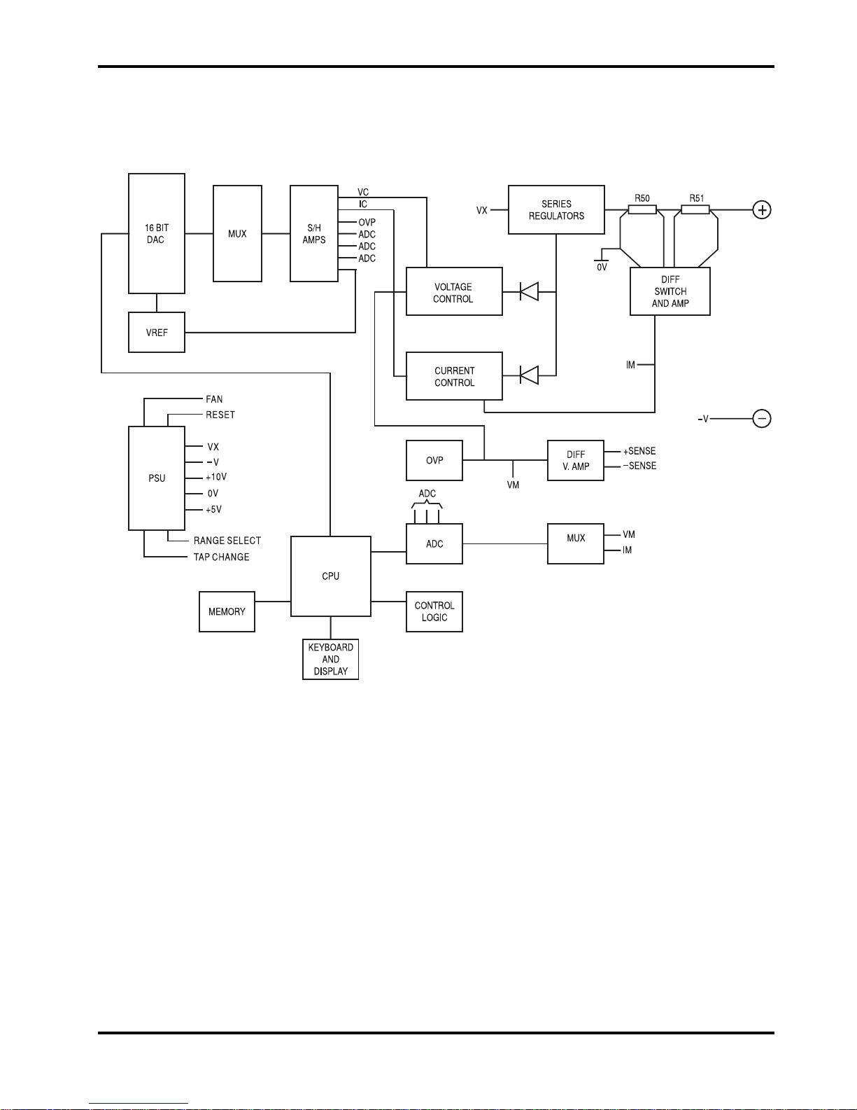
Block Diagram
31
Page 33

Interconnection Diagram
Single PSU
Triple PSU
32
Page 34

Component Layouts
Control Pcb
33
Page 35

Power Pcb
34
Page 36

Main Terminal Pcb
Auxiliary Power Pcb (Triple only)
Auxiliary Terminal Pcb (Triple only)
35
Page 37

Interface Pcb
Keyboard/Display Pcb (Single)
36
Page 38

Keyboard/Display Pcb (Triple)
37
Page 39

Circuit Diagrams
AC Supply Connection Pcb
Main Output Front Panel
Terminal Pcb
38
Page 40

DAC, ADC Sample & Hold ccts,
error logic.
Control Pcb Sheet 1of 2
Page 41

Voltage & Current Control,
OVP & Sense fault trip.
Control Pcb - Sheet 2of 2
Page 42

Power Output, Internal Supplies,
Fan Control, System reset.
Power Pcb (35V/3A) - Sheet 1of 2
Page 43

Microcontroller, Keyboard
and Display interfaces.
Power Pcb (35V/3A) - Sheet 2of 2
Page 44
Power Output, Internal Supplies,
Fan Control, System reset.
Power Pcb (56V/2A) - Sheet 1of 2
Page 45

Microcontroller, Keyboard
and Display interfaces.
Power Pcb (56V/2A) - Sheet 2of 2
Page 46

Interface Pcb
Page 47

Keyboard & Display Pcb - Single
Auxillary Power - Front panel terminal Pcb
(Triple only)
(Triple only)
Auxillary Power - Power Pcb
Page 48

Keyboard & Display Pcb - Triple
Output 2Output 1
 Loading...