

Page 1

CPX200
Dual 35V 10A
Power Supply
Service Manual
Book Part Number 48511-0270 - Issue 1
Page 2

Table of Contents
Specifications 2
Safety 4
EMC 5
General 6
Circuit Descriptions 7
Calibration 12
Parts List 14
Component Layouts 22
Circuit Diagrams 25
1
Page 3
Specifications
OUTPUT SPECIFICATIONS
Voltage Range: 0V to 35V
Current Range: 0A to 10A
Power Range: Up to 175W
Output Voltage Setting: By coarse and fine controls.
Output Current Setting: By single logarithmic control.
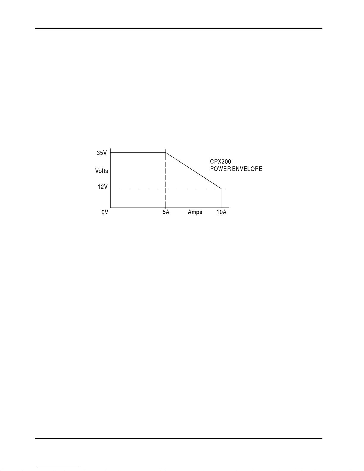
Operating Mode: Constant voltage or constant current with automatic cross-over
provided that the power demanded stays within the power
envelope, see graph. Outside of this envelope the output becomes
unregulated.
Output Switch: Electronic. Preset voltage and current displayed when off.
Output Terminals: 4mm terminals on 19mm (0·75”) pitch. 15A max.
Sensing: Remote via 4mm terminals or direct via shorting links (provided).
Output Impedance:
Typically <5mΩ in constant voltage mode.
Typically >5kΩ in constant current mode (voltage limit at max).
Output Protection: Forward protection by Over-Voltage Protection (OVP) trip;
maximum voltage that should be applied to the terminals is 50V.
Reverse protection by diode clamp for reverse currents up to 3A.
OVP Range: 10% to 110% of maximum output voltage set by front panel
screwdriver adjustment.
Load & Line Regulation: <0.01% of maximum output for a 90% load change or 10% line
change.
Ripple & Noise
(20MHz bandwidth):
5mVrms max; typically <2mVrms, <20mV pk-pk, both outputs fully
loaded (7A @ 25V), CV mode.
Transient Load Response: <2ms to within 100mV of set level for 90% load change.
Temperature Coefficient: Typically <100ppm/°C
Status Indication: Output on lamp.
Constant voltage mode lamp.
Constant current mode lamp.
Unregulated (power limit) lamp
Trip message on display.
2
Page 4

METER SPECIFICATIONS
Meter Types: Dual 4 digit meters with 12.5mm (0.5") LEDs. Reading rate 4 Hz.
Meter Resolutions: 10mV, 10mA
Meter Accuracies: Voltage 0.2% of reading +/-1 digit,
Current 0.5% of reading +/-1 digit
GENERAL
AC Input: 230V AC ± 14%, 50/60Hz. Installation Category II.
Power Consumption: 600VA max.
Operating Range: +5ºc TO +40ºC, 20% TO 80% RH.
Storage Range: -40ºC to + 70ºC.
Environmental: Indoor use at altitudes up to 2000m, Pollution Degree 1.
Safety: Complies with EN61010-1.
EMC: Complies with EN50081-1 and EN50082-1.
Size: 210 x 130 x 350mm (WxHxD) half rack width x 3U height
(optional rack mounting kit available).
Weight: 5kg
3
Page 5

Safety
This power supply is a Safety Class I instrument according to IEC classification and has been
designed to meet the requirements of EN61010-1 (Safety Requirements for Electrical Equipment
for Measurement, Control and Laboratory Use). It is an Installation Category II instrument
intended for operation from a normal single phase supply.
This instrument has been tested in accordance with EN61010-1 and has been supplied in a safe
condition. This instruction manual contains some information and warnings which have to be
followed by the user to ensure safe operation and to retain the instrument in a safe condition.
This instrument has been designed for indoor use in a Pollution Degree 1 environment (no
pollution, or only dry non-conductive pollution) in the temperature range 5°C to 40°C, 20% - 80%
RH (non-condensing). It may occasionally be subjected to temperatures between +5° and -10°C
without degradation of its safety.
Use of this instrument in a manner not specified by these instructions may impair the safety
protection provided. Do not operate the instrument outside its rated supply voltages or
environmental range. In particular excessive moisture may impair safety.
WARNING! THIS INSTRUMENT MUST BE EARTHED
Any interruption of the mains earth conductor inside or outside the instrument will make the
instrument dangerous. Intentional interruption is prohibited. The protective action must not be
negated by the use of an extension cord without a protective conductor.
When the instrument is connected to its supply, terminals may be live and opening the covers or
removal of parts (except those to which access can be gained by hand) is likely to expose live
parts. The apparatus shall be disconnected from all voltage sources before it is opened for any
adjustment, replacement, maintenance or repair. Capacitors inside the power supply may still be
charged even if the power supply has been disconnected from all voltage sources but will be
safely discharged about 10 minutes after switching off power.
Any adjustment, maintenance and repair of the opened instrument under voltage shall be avoided
as far as possible and, if inevitable, shall be carried out only by a skilled person who is aware of
the hazard involved.
If the instrument is clearly defective, has been subject to mechanical damage, excessive moisture
or chemical corrosion the safety protection may be impaired and the apparatus should be
withdrawn from use and returned for checking and repair.
Make sure that only fuses with the required rated current and of the specified type are used for
replacement. The use of makeshift fuses and the short-circuiting of fuse holders is prohibited.
Do not wet the instrument when cleaning it.
The following symbols are used on the instrument and in this manual:-
Earth (ground) terminal.
mains supply OFF.
l
mains supply ON.
alternating current (ac)
direct current (dc)
4
Page 6

EMC
This power supply has been designed to meet the requirements of the EMC Directive
89/336/EEC.
Compliance was demonstrated by meeting the test limits of the following standards:
Emissions
EN50081-1 (1992) Generic emission standard for residential commercial and light
industry. Test methods and limits used were:
a) EN55022 Conducted, Class B
b) EN55022 Radiated, Class B
Immunity
EN50082-1 (1992) Generic immunity standard for residential, commercial and light
industry. Test methods and limits used were:
a) EN60801-2 (1993) Electrostatic Discharge, 8 kV air discharge.
b) IEC801-3 (1984) RF Field, 3 V/m.
c) IEC801-4 (1988) Fast Transient, 1 kV peak (AC line) and 0.5kV peak (DC outputs).
Note that electrostatic discharge direct to the output terminals will not damage the instrument but
may trip the Overvoltage Protection (OVP), turning the output off, see Protection section.
Note also that if the power supply is operated in a high RF field, the RF signal will be picked up
on unscreened leads between the supply and the load. If the load is likely to be sensitive to such
signals, connect it to the supply using screened leads.
Cautions
To ensure continued compliance with the EMC directive the following precautions
should be observed:
a) after opening the case for any reason ensure that all signal and ground connections
are remade correctly before replacing the cover. Always ensure all case screws are
correctly refitted and tightened.
b) In the event of part replacement becoming necessary, only use components of an
identical type, see the Service Manual.
5
Page 7

General
Service Handling Precautions
Service work or calibration should only be carried out by skilled engineers using high quality test
equipment. If the user is in any doubt as to his competence to carry out the work, the instrument
should be returned to the manufacturer or their agent overseas for the work to be carried out.
The tracks on the printed circuit boards are very fine and may lift if subjected to excessive heat.
Use only a miniature temperature-controlled soldering iron and remove all solder with solder wick
or suction before attempting to remove a component.
Dismantling the instrument
WARNING
Disconnect the power supply from all voltage sources before it is opened for adjustment or repair.
Capacitors inside the supply may still be charged even if the supply has been disconnected from
all voltage sources but will be safety discharged about 10 minutes after removing power.
If any adjustment or repair of the opened supply under voltage is inevitable it shall be carried out
only be a skilled person who is aware of the hazard involved. The incoming AC supply to the unit
under test should be isolated for safety by means of a 1:1 isolation transformer of at least 700VA.
High voltages (up to 400V) are always present in the primary-side circuitry which lies in a clearly
defined area at the rear of both the upper (control) and lower (main) printed circuit boards.
Removing the link at PJ10 only disconnects HV from the power FETs Q1/Q2 (Q101/Q102).
1. Remove the six screws retaining the top cover.
2. To remove the upper (control) pcb proceed as follows.
Unplug the 26-way flat cables to the front panel pcb and the 16-way flat cables to the
lower (main) pcb noting their orientation (red stripe to pin 1 corner markers on pcb).
Unplug the harnesses from the 50Hz transformer (PJ7, PJ107) and the control
connections to the main board (PJ5, PJ105) noting the orientation of the sockets (pin 1 on
the socket housing to pin 1 corner markers on pcb).
Remove the 4 self-tap screws and lift off the pcb.
3. To remove the lower (main) pcb proceed as follows. Remove the power (M3 nuts) and
sense (2-way header) connections to the front panel for both channels noting orientation;
inner (insulated) power lead is positive, red sense lead to corner marker on pcb.
Unplug the two harness connections from the 50Hz transformer (PJ1 and PJ8) and the
connection from the front panel switch (PJ6), noting orientation (pin 1 on the socket
housing to pin 1 corner markers on pcb). Remove the safety earth connection to the rear
panel; remove the rear panel (3 screws). Remove the 9 screws which secure the main pcb
support pillars to the case lower (i.e. the screws accessible underneath the case lower)
and lift the pcb clear with its mounting pillars attached.
4. To remove the front panel pcb, first remove the six push-on control knobs then undo the 5
screws securing the pcb to the front panel and lift free.
5. Reassemble in the reverse order taking great care to ensure that all connections are
exactly as before dismantling and that no insulation creepage and clearance distances
have been compromised. Ensure that only the correct fastenings are used otherwise
earthing, and hence EMC and safety performance, may be impaired.
6
Page 8

Circuit Descriptions
The two outputs are identical with the exception of slight layout variations; only one output
(Channel A) is therefore described. Component positions on the other output (Channel B) are
numbered from 101 upwards, e.g. C22 on Channel A described is C122 on Channel B.
Power Section
The power section is contained entirely on the main (lower) board; refer to the main pcb
schematic.
Each output is configured as a double-ended half-bridge operating in continuous flyback mode to
reduce switching currents in the power FETs and output diodes; both converters operate from a
common high voltage (rectified mains) supply.
The secondary power limit is determined by the primary current limit which gives rise to a linear
characteristic (between maximum current and maximum voltage) rather than a parabolic
characteristic associated with a true ‘constant power’ limit, see Specification section.
Mains Input, Filtering and Rectification
The AC input to the supply is direct via a pcb-mounted IEC inlet connector. Components C9, L3,
L4, and C5-C8 comprise an input filter which ensures that the supply meets both conducted
emission and conducted immunity EMC requirements. VDR1 ‘clips’ mains spikes for component
protection; R3 provides safety discharge for C9, C5 and C8.
Pcb-mounted fuse FS1 limits damage on switchmode failure; the front panel mains switch is
connected via PJ6; RT1 reduces the mains inrush current when the unit is turned on from cold.
BRI is a bridge rectifier and C1, C2 the reservoir capacitors for the high voltage rail which is
linked at PJ10 to VBULKA and VBULKB of Channel A and Channel B respectively. L1 and L2
reduce current spikes caused by the switching of the FETs. BR1 and C1, C2 can also be
configured as a voltage doubler for 115VAC operation by fitting the header into PJ1B instead of
PJ1A; however, for operation up to full power (350W) L3 and L4 must be changed to 8Amp
components. PJ1 is also the point from which mains power is fed to the auxiliary mains
transformer.
Operation of the Double-ended Half-bridge
A simplified version of the power switching stage is shown below.
When FETs Q1 and Q2 are turned on, current flows in the primary winding of power transformer
T1, storing energy in the primary inductance; D3 and D4 are reverse-biased so no current flows in
7
Page 9

the secondary. When Q1 and Q2 are turned off the voltage across the primary will reverse and
generally bring diodes D1 and D2 into conduction; D1, D2 provide clamp protection against
overvoltage caused by leakage inductance in the transformer, so protecting the FETs. At the
same time the secondary e.m.f. generated will cause current to flow through D3, D4 into C14 and
the load; as soon as this starts to happen current will cease to flow through D1 and D2 and the
energy stored in the primary is transferred to the secondary.
Zener diodes D7 and D8 protect the FETs in the event of a voltage surge and protect the drive
circuit in the event of a FET failure.
FET Drive Circuit
IC1 is an IR2110 drive IC which has the necessary on-chip isolation (500V) to be able to drive
both FETs. The FETs need 15V gate drive. The 15V supply for Q2 is generated from the auxiliary
mains transformer via BR2 and IC16; this rail also powers all the ground-referenced control
circuitry on the primary side, including the UC3846. Q1 needs an isolated supply which is
generated from an extra winding on the power transformer in phase with the secondary; D5 and
C23 rectify and smooth the transformer output, dropper resistor R15 and 15V zener D9 regulate
the rail.
Until the FETs start switching no 15V supply for Q1 is generated. To overcome this R21 is used to
charge C23 at start-up; when VBULKA reaches about 150V there is enough voltage on C23 to
turn on the high rail of IC1 and maintain the FET in an oscillating mode independent of output
loading. If for any reason this rail should drop below 8V, IC1 will switch off, thus maintaining a
good enhancement voltage across the gate at all times.
R8, C10 and R9, C11 are snubber networks for Q1 and Q2 respectively.
Output Filtering
Large switching spikes caused by the switching of FETS Q1, Q2 and rectifying diodes D3, D4 are
filtered by the output stage to bring both differential noise and common mode noise into
specification.
Snubber network R10, C13 reduces noise generated by the output diodes.
L5 and C16 comprise the main differential filter; R16 damps any ringing in the filter. R13, R17 and
R20 are a small pre-load, ensuring voltage loop control with no external load and providing some
load for the L5, C16 filter. The common mode filter L7, C15/C27 further reduces differential noise.
Common-mode noise is minimised by the low capacitance design of power transformer and is
attenuated by C17, C18; R19 provides a discharge path for these capacitors when the output
terminals are floated from ground. Solid ground connections at E1 and E2 are essential for good
common-mode noise performance.
The front panel mounted components LLA, CAA and CAB provide both differential and commonmode attenuation at high frequencies (>2MHz); HF differential noise is attenuated by the leakage
inductance of LLA with CAB and HF common-mode noise is attenuated by LLA and CAA.
8
Page 10

Control Section
The control circuitry is contained entirely on the control (upper) board with the exception of the
current transformer (T2) which is fitted on the main board and the user controls themselves which
are on the front panel board.
Voltage Control Loop
The feedback voltage for the voltage control loop is fed from the main board via PJ4 pin 5
(+SENSE A) and PJ4 pin 8 (-SENSE A); R12/C21 and R11/C19 (all on the main board) ensure
stability when long leads are used with remote sense. Usual operation is with the sense
connections made directly at the output terminals but up to 1V drop in the connecting leads can
be corrected for by sensing remotely. PTC1 and PTC2 (on the main board) provide an alternative
permanent sense connection if no other sense connection is made. If, during remote sense
operation, the output terminals become disconnected from the load, PTC1 and PTC2 also provide
current limiting protection when the load attempts to draw current from the sense terminals.
IC2 buffers and inverts the front panel voltage controls VR1, VR2 to give approximately –2·62V at
maximum output (35V). IC1 is a differential amplifier with a voltage gain of 13·3 set by R18, R20
and R19, R21, VR4. VR4 trims the differential gain which ensures voltage regulation is
maintained during remote sense operation when there is a voltage difference between –SENSE
and –OUTPUT, see Calibration section. The output of the op. amp. IC1 drives the input diode of
the opto coupler OPT1. This is a low noise device and helps to prevent switching noise and pickup from getting into the control loop. The output of the opto-coupler drives current through R13;
the voltage developed across R13 is fed to IC5 pin 5 the input of the error amplifier of the PWM
controller, IC5. This amplifier is configured as a voltage follower with a gain of one. IC5 then
converts this input signal into a pulse width modulated squarewave which is used to drive the two
power FETs Q1 and Q2, via IC1 (all on the main board).
Current Control Loop
The current control loop uses the voltage across the current sense resistor R14 (main board)
which is fed to the control board via PJ4 pin 7 (ISENSE+A) and PJ4 pin 2 (ISENSE-A). IC6
provides a gain of 10 and its output is fed to the high gain amplifier IC17, the other input of which
(ISETA) is derived from the front panel current limit control, VR4, via PJ8 pin 2. When the current
sensed through R14 is below the set level, the output of IC17 is high, driving the maximum
current into opto OPT3 via R6 which in turn develops the maximum voltage across R11 at pin 1 of
IC5. When the output current approaches the set level the output of IC17 falls and the voltage
across R11 drops. This voltage is fed to IC4 pin 1, the current limit adjust input of the PWM
controller, and acts to reduce the peak current in the primary as the voltage across R11 falls,
irrespective of the voltage control loop.
Overvoltage Protection (OVP)
The overvoltage trip point is set by preset VR3 on the front panel board (it is a screwdriver
adjustment through the front panel). This voltage (OVPSETA) is fed via PJ8 pins 4 and 8 to the
inverting input of comparator IC4-C; the output voltage (OVPDETECT+A) is sensed at the
common-mode choke L7 (main board) and fed to the other input of IC4-C via PJ4 pin 6. When the
output voltage exceeds the set OVP the output of IC4-C goes high, turning on Q4 and Q3 which
latches the comparator in the high state. When the comparator output goes high, current is driven
into the opto OPT2 via D9; the output of the opto goes to 5V, pulling pin 16 of IC5 high which
shuts it down. The power supply needs to be switched off to allow the OVP circuit to reset.
9
Page 11

Primary Current Control and Primary Current Limit
The primary current is sensed by transformer T2 on the main board; the primary is in series with
T1 and the secondary is fed to D2/R2 on the control board via PJ5 pins 1 and 2. D2 rectifies the
signal which appears as a voltage across R2 in parallel with VR5/R22; R1 and D1 allow the
current transformer to be reset on each cycle. The ramp voltage developed across R22,
corresponding to the ramp current in the primary of T1/T2, is fed to IC5 pin 4, the +current sense
input of the PWM controller, via VR5/R22. This arrangement provides pulse-by-pulse primary
current control, giving better overall voltage loop control by improving line regulation and load
response.
In normal operation the pulse is terminated at a point determined by the voltage on IC5 pin 5, the
error amplifier input; the greater the demand from the voltage control loop via the error amplifier,
the higher the primary current will ramp before the pulse is terminated. There is, additionally, an
overriding limit mechanism in IC5 which terminates the pulse when the ramp at pin 4 reaches a
certain level, regardless of a demand for more power by the signal on pin 5. Since VR5 ‘scales’
the voltage applied to IC5 pin 4, VR5 effectively sets the primary current limit which in turn sets
the secondary power limit, see Calibration section.
Front Edge Blanking
Front edge blanking is provided by Q1, C2, R4, D24 and C3. Front edge blanking prevents the
switching spikes caused by main board FETs Q1 and Q2 being fed into pin 4 of IC5 via the
primary current limit circuit (T2, D2, R2, VR5, R22 and R3).
Measurement and Display
The measurement system and display are controlled by a microcontroller IC11. The measurement
of output and preset values of voltage, current and OVP is performed by the 12 bit analog to
digital converter IC12. The measurement rate is controlled by the 4·0MHz ceramic resonator XL1
connected between pins 22 and 23 and the buffered version of this 4MHz signal at pin 25 is used
as the clock to the microcontroller IC1. The ADC, IC12, is a dual slope converter and provides
just over 8 readings per second when clocked at 4MHz. The ADC is run in continuous mode and
the status signal on pin 2 is read by the microcontroller every 6ms. When a reading is ready the
microcontroller reads the 12 bit binary value and then converts it to 7 segment BCD and stores it
ready to be sent to the display. After each reading the microcontroller switches the input
multiplexers IC13 and IC14 to the next required input. In this way it is possible to read and display
any of the following:
Preset Volts
Preset Current
OVP
Output Volts
Output Current
The multiplexers are controlled by the latch, IC6, on the front panel board which also drives the
additional indicator LEDs; this latch is driven by the microcontroller, IC11.
The decision on what to measure and display at any time is taken by the microcontroller and in
order to do this correctly a number of status signals and switches are monitored on a regular
basis. These are:
VLIMDA from IC4-B
ILIMDA from IC4-A
OVPTRIPA the OVP trip signal
OVPKEYA the OVP key signal
OUTPUTA the output on/off switch signal
All these signals may be read by the microcontroller as required.
10
Page 12

The +2·45V reference line VREF+A is derived from reference diode D23 attenuated to about
188mV by divider R83, R82 at the reference input of analogue to digital converter IC12, yielding a
sensitivity of about 92uV per digit.
The set current signal ISETA is taken from the VR4 wiper on the front panel board via PJ8 pin 2
and on to the ADC as IPROGA, via adjustable attenuating chain R92, VR3, R93, for display of the
preset current level.
The voltage control signal VSETA is derived from the wipers of the coarse and fine voltage
controls VR1 and VR2 on the front panel board via PJ8 pin 3 and on to the ADC as VPROGA via
adjustable attenuating chain R88, VR7, R89, for display of preset voltage level.
The OVP front panel preset potentiometer VR3 is fed from the reference voltage defined by zener
D4. The OVP set from VR3 wiper, OVPSETA, is fed via PJ8 pin 4 and on to the ADC input via
divider R90, R91 for display of preset over voltage trip level.
Actual output volts are fed from the main board, via PJ4 pin 9 (+VESENSEA) and PJ4 pin 10 (–
VESENSEA), to attenuating chain R78, VR8 and R80 and on to the ADC.
The voltage across the current sense resistor, attenuated by R18 and VR1 (main board) is fed via
PJ4 pin 1 (O/P CURRENT SENSE +A) and PJ4 pin 2 (O/P CURRENT SENSE –A) to the ADC.
11
Page 13

Calibration
Refer to the General section for dismantling instructions and safety precautions. Component
numbers are given for Channel A/Channel B, e.g. VR1/VR101, where VR1 refers to Channel A
and VR101 to Channel B. Channel A is marked as Output 1 on the front panel, Channel B as
Output 2. All adjustments are on the control board unless otherwise stated.
Equipment Required
5½ digit multimeter with better than 0·05% DC Volts accuracy and better than 0·1% DC Amps
accuracy (to 10A); alternatively use a precision shunt for current measurement.
Rheostat or other high power load arrangement to provide up to 5A load at 35V and 10A and 12V.
A small switch, 15kΩ resistor and diode.
Voltage Calibration
Connect DMM, set to Volts, across output. Set voltage controls to minimum and current control to
maximum. Switch output ON and check for a reading of 00·00V ± 0·01V on display and DMM.
Set voltage controls to maximum. Adjust VR16/VR116 (maximum output volts) for a reading of
35·30V ± 0·02V on the DMM. Adjust VR2/VR102 (preset volts) until display matches DMM.
Connect rheostat to output and adjust for nominally 4A at maximum output voltage. Reduce
current limit (current control anticlockwise) until output just enters CI mode. Adjust VR8/VR108
(measured volts) until display matches DMM reading.
Current Calibration
Connect DMM, set to 20A range, in series with rheostat set to about 1Ω. With output OFF set
voltage controls to maximum and current control to 0·10A. Switch output ON and adjust
VR1/VR101 for 0·10A ± ·01A on DMM.
Set voltage controls to 12V, current control to maximum; supply should be in CI mode. Adjust
VR6/VR106 (maximum output current) for 10·20A ± ·02A on DMM.
Switch output OFF. Adjust VR3/VR103 (preset current) until display matches maximum output set
by VR6/VR106 above.
Increase rheostat resistance until unit enters CV mode. Adjust VR1/VR101 (measured current) on
main board until display matches DMM reading.
Set Power Limit
Switch output OFF, set voltage control to 12·1V, current control to maximum. Switch output ON,
set rheostat so that current is 10·0A (ensure CV mode is maintained). Adjust VR5/VR105 (power
limit) until the UNREG l.e.d. just lights; back off VR5/VR105 until CV is lit and UNREG is off.
Set voltage controls to maximum and check unit enters UNREG mode. Increase rheostat
resistance until unit enters CV mode again; check meter reads between 5A and 6·2A.
Remove load.
OVP Calibration
Set voltage controls to minimum, current control to maximum. Set VR7/VR107 fully anticlockwise. Switch output ON. Press OVP button and set front panel OVP control (screwdriver
adjustment) for a display of 20·00V; release OVP button.
Set output voltage to 20·00V and adjust VR7/VR107 (OVP calibrate) slowly anticlockwise until
OVP is tripped (display reads TRIP). Turn output OFF and reset front panel OVP control fully
clockwise.
12
Page 14

Differential Gain Adjustment
Remove the link between the –OUTPUT and –SENSE terminals and fit a diode, anode to
–SENSE and cathode to –OUTPUT; connect a small switch across the diode. Leave the link in
place between +OUTPUT and +SENSE and connect a 15kΩ resistor between +OUTPUT and
–SENSE. Connect the DMM, set to Volts, between the sense terminals.
Close the switch, switch the output ON and set the output to approximately 17V; note the exact
reading. Open the switch and adjust VR4/VR104 for exactly the same reading; close the switch
again and check the reading is unchanged.
Remove the diode, resistor and switch and refit the sense link.
Noise Measurements
Differential and common-mode noise checks can be made using the arrangement below. Keep all
unscreened connections as short as possible.
Make measurements with the output fully loaded (e.g. 25V @ 7A). Measure differential and
common-mode noise one at a time on a 20MHz TRMS voltmeter or use a 20MHz bandwidthlimited scope for peak-to-peak measurements.
13
Page 15

Parts List
PCB ASSY FRONT PANEL - (44115-0820)
Part Number Description Position
22226-0140 KEYSWITCH DARK GREY K1,2,101,102
22573-0056 HEADER 16 WAY STR SIL FOR DISPLAYS
23202-0270 RES 27R0F W25 MF 50PPM R1-8,101-108
23202-1910 RES 910RF W25 MF 50PPM R21,121
23202-2150 RES 1K50F W25 MF 50PPM R17,18,38,39,117,118,138,139
23202-3100 RES 10K0F W25 MF 50PPM R19,31,40,119,131,140
23202-3470 RES 47K0F W25 MF 50PPM R9,12,109,112
23202-4470 RES 470KF W25 MF 50PPM R20,120
23347-0140 POT 10K LIN VR1,2,101,102
23347-0150 POT 10K LOG VR4,104
23382-3100 RES PS/H10K CERMET MIN VR3,103
23557-0658 CAP 100U 25V ELEC P2.5 C1,101
23620-0246 CAP 100NK 63V P/E P5 C2,15-19,102,115-119
25061-0200 LED - T1 ROUND (3MM) - RED LED1-4,101-104
25061-9503 DISPLAY - 4 DIGIT LED DISP1,2,101,102
27164-0506 IC ULN-2803A IC8,108
27231-2730 IC 74HC273 IC6,7,106,107
27234-5730 IC 74AC573 IC5,10,105,110
35555-2260 PCB - FRONT PANEL
PCB ASSY CNTL - (44115-0810)
Part Number Description Position
20030-0263 WASHER M3 ZPST FOR IC8/9,108/109
20038-9501 WASHER M3 SPRING FOR IC8/9,108/109
20210-0101 NUT M3 ZPST FOR IC8/9,108/109
20234-0011 SCREW M3 X 10 PNHDPZ NPST FOR IC8/9,108/109
20611-0003 BUSH POLYESTER TO220 J22-5006 FOR IC8,108
20613-0006 WASHER (SIL-PAD) TO220 FOR IC8/108
20661-0800 SPACER TRANSISTOR MTG TO18 FOR IC3,103
20670-0130 HEATSINK PCB MTG 25MM HIGH HS1,101
20670-9002 T0220 CLIP ON HEATSINK FOR IC10,110
22315-0440 FUSE 375mAT SUBMIN PCB MTG FS3,4,103,104
22315-0452 FUSE 1.0AT SUBMIN PCB MTG FS1,2,101,102
22573-0205 HEADER 5 WAY STRAIGHT .156P PJ5,7,105,107
22574-0122 SKT DIL 28 PIN FOR IC11,111
14
Page 16

PCB ASSY CNTL – (44115-0810) continued/.....
Part No. Position Description
22575-0062 HEADER 10 WAY (2X5) STR PJ4,104
22575-0064 HEADER 26 WAY (2X13) STR PJ8,108
23185-0000 RES ZERO OHM LK2,7,8,102,107,108
23189-0560 RES 56RJ 1W6 500PPM TYPE PR37 R2,102
23190-1100 RES 100RJ 2W5 500PPM TYPE PR52 R15,115
23202-0220 RES 22R0F W25 MF 50PPM R84,184
23202-1470 RES 470RF W25 MF 50PPM R55,155
23202-1750 RES 750RF W25 MF 50PPM R12,22,112,122
23202-2100 RES 1K00F W25 MF 50PPM R3,17,39,57,61,68,95,96,103,117,139,
157,161,168,195,196
23202-2150 RES 1K50F W25 MF 50PPM R6,94,106,194
23202-2200 RES 2K00F W25 MF 50PPM R13,72,113,172
23202-2240 RES 2K40F W25 MF 50PPM R10,110
23202-2300 RES 3K00F W25 MF 50PPM R97,197
23202-2360 RES 3K60F W25 MF 50PPM R91,191
23202-2390 RES 3K90F W25 MF 50PPM R44,144
23202-2430 RES 4K30F W25 MF 50PPM R46,146
23202-2470 RES 4K70F W25 MF 50PPM R5,23,28,29,33,36,37,48,73,105,123,128,
129,133,136,137,148,173
23202-2560 RES 5K60F W25 MF 50PPM R11,111
23202-2680 RES 6K80F W25 MF 50PPM R21,121
23202-2750 RES 7K50F W25 MF 50PPM R20,120
23202-2820 RES 8K20F W25 MF 50PPM R80,180
23202-3100 RES 10K0F W25 MF 50PPM R7,38,40,41,43,49,59,60,64,71,79,82,85,
107,138,140,141,143,149,159,160,164,
171,179,182,185
23202-3120 RES 12K0F W25 MF 50PPM R9,109
23202-3180 RES 18K0F W25 MF 50PPM R30,130
23202-3200 RES 20K0F W25 MF 50PPM R16,54,116,154
23202-3220 RES 22K0F W25 MF 50PPM R66,166
23202-3270 RES 27K0F W25 MF 50PPM R8,108
23202-3300 RES 30K0F W25 MF 50PPM R74,174
23202-3330 RES 33K0F W25 MF 50PPM R75,76,175,176
23202-3360 RES 36K0F W25 MF 50PPM R89,93,189,193
23202-3430 RES 43K0F W25 MF 50PPM R26,126
23202-3470 RES 47K0F W25 MF 50PPM R42,47,77,81,90,142,147,177,181,190
23202-3560 RES 56K0F W25 MF 50PPM R27,127
15
Page 17

PCB ASSY CNTL - (44115-0810) continued/...
Part No. Position Description
23202-4100 RES 100KF W25 MF R18,19,86,87,118,119,186,187
23202-4120 RES 120KF W25 MF 50PPM R83,183
23202-4160 RES 160KF W25 MF 50PPM R53,153
23202-4200 RES 200KF W25 MF 50PPM R34,88,134,188
23202-4750 RES 750KF W25 MF 50PPM R14,114
23202-4820 RES 820KF W25 MF 50PPM R92,192
23202-5100 RES 1M00F W25 MF 50PPM R78,178
23206-1470 RES 470RF W6 MF 50PPM R4,104
23210-3100 RES 10K0J 2W MF 250PPM R1,101
23301-0457 RES NETWK SIL 47K X 4S RP4,104
23377-1470 RES PS/H 470R CF 10MM VR5,105
23377-2100 RES PS/H1K0 CF 10MM VR4,104
23377-2220 RES PS/H2K2 CF 10MM VR6,106
23377-2470 RES PS/H4K7 CF 10MM VR7,107
23377-3100 RES PS/H10K CF 10MM VR16,116
23377-3220 RES PS/H22K CF 10MM VR1,101
23379-2220 RES PS/H2K2 Cermet 10MM VR8,108
23379-3100 RES PS/H10K Cermet 10MM VR2,3,102,103
23427-0331 CAP1N0K 63V CER HI K P5 C16,116
23427-0374 CAP 100PJ 100V CER N150 P2.5 C3,18,103,118
23427-0384 CAP 220PK 100V CER MED K P2.5 C2,102
23557-0611 CAP 47U 10V ELEC P2 C48,50,148,150
23557-0612 CAP 1U0 50V ELEC P2 C10,21,42,110,121,142
23557-0658 CAP 100U 25V ELEC P2.5 C25,26,36,125,126,136
23557-0660 CAP 2200U 16V ELEC P5 C13,113
23557-0664 CAP 1000U 35V ELEC P5 C27,29,127,129
23620-0245 CAP 4N7K 63V P/E P5 C8,108
23620-0246 CAP 100NK 63V P/E P5 C1,6,11,12,14,15,17,19,20,23,28,
30-33,35, 38-40,47,49,54,101,106,111,
112,114,115, 117,119,120,123,128,
130-133, 135,138-140,147,149,154
23620-0247 CAP 220NK 63V P/E P5 C22,122
23620-0249 CAP 330NK 63V P/E P5 C46,146
23620-0252 CAP 2N2K 63V P/E P5 C7,107
23620-0256 CAP 1U0K 63V P/E P5 C43,51,52,143,151,152
23620-9007 CAP 10NK 100V P/E P5 C5,9,34,105,109,134
23621-0310 CAP10NJ 400V P/E P7.5 C44,144
PCB ASSY CNTL - (44115-0810) continued/...
16
Page 18

Part No. Position Description
23685-0002 CAP 1N0J 100V P/P C4,104
23685-0007 CAP 100NK 160V P/P P10 C45,145
25021-0901 DIO 1N4148 B/R D1,2,3,5,6,8,9,11-17,24,101,102,103,105,
106,108,109, 111-117,124
25115-0907 DIO 1N4002 B/R D7,10,107,110
25130-0903 DIO ZEN 5V1 W4 D4,104
25211-9302 RECTIFIER BRIDGE W02G BR1,101
25336-5590 TRAN PNP BC559C Q3,103
25380-0229 TRAN NPN BC549 Q2,4,5,102,104,105
25601-0470 TRAN MOSFET N CHAN 2N7000 Q1,101
27001-0020 OPTO-COUPLER CNY17-3 OPT2,102
27001-0030 OPTO-COUPLER HCPL-4503 OPT3,4,103,104
27103-0020 IC LM339 IC4,104
27106-0520 IC OP-07 IC1,2,6,17,101,102,106,117
27153-0030 IC 7109 IC12,112
27160-0014 IC V/REG 7905 IC10,110
27160-0017 IC V/REG 7812 IC8,108
27160-0440 IC V/REG LM2940CT5 IC9,109
27161-0120 IC V/REF ZN404/ZRA245 2.45V D23,123
27168-0020 IC UC3846N IC5,105
27226-0510 IC 4051B IC13,14,113,114
27250-2000 IC MCU8 PIC16C55XT-P IC11,111
28502-0010 RESONATOR CER 4MHZ CSA4.00MG XL1,101
35555-2250 PCB - CONTROL
PCB ASSY - MAIN (44115-0800)
Part Number Description Position
20030-0263 WASHER M3 ZPST FOR D3,4,103,104, PCB, IEC
20037-0301 WASHER M3 SHK/PROOF I/T ZPST E,E1,E2
20038-9501 WASHER M3 Spring FOR D3,4,103,104, PCB, IEC
20062-9303 SCREW NO 6x0.5in. PNHDPZ ST/AB FOR SK1,101
20062-9305 SCREW No.6x3/4in. Pozi. Pan MAIN/CONTROL PCB PILLARS
20205-0610 STUD M3 X 10 KFH-M3-10ET W3,4,103,104, IEC INLET
20210-0101 NUT M3 ZPST FOR D3,4,103,104, IEC INLET
20234-0025 SCREW M3 X 12 PNHDPZ ZPST FOR D3,4,103,104
20234-0027 SCREW M3 X 6 PNHDPZ ZPST FOR PCB SPACERS
17
Page 19

PCB ASSY - MAIN (44115-0800) continued/...
Part No. Position Description
20611-0003 BUSH POLYESTER TO220 J22-5006 FOR D3,4,103,104
20613-0012 WASHER NON-INSULATING FOR Q1,2,101,102
20613-9401 WASHER TO220 ADHESIVE FOR D3,4,103,104
20661-0225 SPACER Hex M3 x 12ZPST FOR PCB
20661-0408 SPACER Rnd/Hex/ST 2.5 L MAIN/CONTROL PCBS
20670-0135 CLIP GP02 FOR PCB MTG H/SINKS FOR Q1,2,101,102
20670-0200 HEATSINK PCB MTG 50MM HIGH SK2,3,102,103
20670-0260 HEATSINK DRILLED M/F -0261 SK1,101
22109-0050 TRANSFORMER HF POWER - CPX T1,101
22109-0070 TRANSFORMER CURRENT SENSE CPX T2,102
22154-0120 CHOKE 10uH AXIAL 35 MILLIOHMS L1,2
22154-0110 CHOKE 130uH/4A L3
22154-0090 CHOKE 10UH/12A - CPX L5,105
22154-0200 CHOKE 1mH/10A COMMON MODE CPX L7,107
22154-0220 CHOKE 3.3mH/4A COMMON MODE L4
22300-0211 FUSEHOLDER PCB MOUNTING FOR FS1
22315-0248 FUSE 10A ANTISURGE (T) HBC CER FS1
22315-0402 FUSE 100mAT TL PCB MTG FS2,102
22520-0160 AC MAINS RECEP 10AMP R/ANG MTG PJ3
22573-0202 HEADER 2 WAY STRAIGHT .156P PJ2,102
22573-0204 HEADER 4 WAY STRAIGHT .156P PJ9
22573-0205 HEADER 5 WAY STRAIGHT .156P PJ5,105
22573-0206 HEADER 6 WAY STRAIGHT .156P PJ10
22573-0207 HEADER 7 WAY STRAIGHT .156P PJ1A,6
22575-0062 HEADER 10 WAY (2X5) STR PJ4,104
23183-3470 RES 47KJ 1W CF R21,121
23183-4100 RES 100KJ 1W CF R1,2
23184-0047 RES 4R7J 2W CF R16,116
23184-2120 RES 1K2J 2W CF R13,17,20,113,117,120
23190-1100 RES 100RJ 2W5 500PPM TYPE PR52 R8,9,10,108,109,110
23202-0270 RES 27R0F W25 MF 50PPM R4,6,104,106
23202-1220 RES 220RF W25 MF 50PPM R11,12,111,112
23202-1330 RES 330RF W25 MF 50PPM R18,118
23202-2100 RES 1K00F W25 MF 50PPM R5,7,105,107
23206-0470 RES 47R0F W60 MF 50PPM R15,115
23206-5680 RES 6M80F W6 MF 50PPM R19,119
PCB ASSY - MAIN (44115-0800) continued/...
18
Page 20

Part No. Position Description
23209-5100 RES 1M00F W75 MF 100PPM R3
23296-0020 RES 0R01D 4 TERM 30PPM PBV R14,114
23379-1100 RES PS/H 100R Cermet 10MM VR1,101
23386-0010 VARISTOR V275LA20A VDR1
23386-0030 THERMISTOR - INRUSH LIMITER 4A RT1
23388-0030 THERMISTOR PTC 2322.661.15693 PTC1,2,101,102
23424-0459 CAP 4N7 250V AC CER Y RATED C6,7
23556-0230 CAP 1000UM 200V ELEC C1,2
23556-0222 CAP 100U 385/400V ELEC C12,112
23556-0225 CAP 2200U 50V ELEC LOW ESR C14,114
23557-0612 CAP 1U0 50V ELEC P2 C22,23,25,122,123,125
23557-0655 CAP 470U 35V ELEC P5 C61,161
23557-0659 CAP 47U 25V ELEC P2 C63,163
23557-0676 CAP 470U 63V ELEC P5 C15,16,115,116
23620-0246 CAP 100NK 63V P/E P5 C19,21,24,26,27,62,119,121,124,126,
127,162
23620-0261 CAP 100NK 400V P/E C17,18,117,118
23620-9007 CAP 10NK 100V P/E P5 C13,113
23684-0010 CAP 470NK 250VAC X2 P/P P27.5 C5,8,9
23687-0010 CAP 1N0F 400V P/P AXIAL C10,11,110,111
25031-0060 DIO BYV27 D5,105
25031-0070 DIO BYV29-400 D1,2,101,102
25031-0080 DIO BYV32E D3, 4,103,104
25117-0020 DIO 1N5401 D6,106
25130-0207 DIO ZEN 15V W4 D9,109
25131-0224 DIO ZEN 18V 1W3 D7, 8,107,108
25211-0302 BRIDGE RECTIFIER D5SB60 BR1
25211-9302 RECTIFIER BRIDGE W02G BR2,102
25601-0440 TRAN MOSFET N CHAN 500V 10A Q1, 2,101,102
27160-0015 IC V/REG 78L15 TO92 (NS) IC16,116
27168-0100 IC IR2110 MOSFET DRIVER IC1,101
35555-2270 PCB - MAIN
19
Page 21

REAR PANEL ASSY - (46912-0520)
Part No. Description Position
20030-0266 WASHER M4 ZPST TRANSFORMER, EARTH
20037-0401 SOLDER TAG SHAKEPROOF - 4BA EARTH
20038-9502 WASHER M4 Spring TRANSFORMER, EARTH
20210-0102 NUT M4 ZPST TRANSFORMER, EARTH
20213-0010 CAPTIVE NUT SNU-1219-17-00
20234-0029 SCREW M4 X 12 PNHDPZ ZPST TRANSFORMER
20236-0010 SCREW M4 X 12 TAMPERPROOF EARTH
22115-0260 TRANSFORMER - CPX200
22575-0204 SKT4W .156 20AWG IDT PJ9
22575-0205 SKT5W .156 20AWG IDT PJ7,107
22575-0207 SKT7W .156 20AWG IDT PJ1A
33331-3540 REAR PANEL PRINTED
FRONT PANEL ASSY - (46912-0510)
Part No. Description Position
20030-0263 WASHER M3 ZPST PCB FIXING
20037-0247 WASHER 4BA SHK/PROOF I/T ZPST GREEN TERMINAL
20037-0305 WASHER 5/16in.SHK/PRF I/T ZPST GREEN TERMINAL
20038-9501 WASHER M3 Spring PCB FIXING
20038-9503 WASHER M3.5 SPRING TERMINALS
20234-0027 SCREW M3 X 6 PNHDPZ ZPST PCB FIXING
20657-0110 KNOB 15MM DA150 006 GREY/99
20657-0111 CAP BLK LINE C157/132 GREY 99
22040-0030 FERRITE SLEEVE APPROX 7/14/15L LLA,LLB
22219-0050 SWITCH ROCKER DPST SOLDER LUGS MAINS SWITCH
22450-0020 EYELET M3.5 (4BA) SHRD BLUE SENSE LEADS
22451-0200 SOLDER TAG 4BA TERMINAL
22571-0670 TERMINAL INSULATED RED TP2
22571-0680 TERMINAL INSULATED BLACK TP2
22571-0690 TERMINAL INSULATED GREEN TP2
22571-0691 WASHER ALUMINIUM FOR TP2E TERM EARTH TERMINAL
22575-0202 SKT2W .156 20AWG IDT PJ2,102
22575-0207 SKT7W .156 20AWG IDT PJ6
23424-0454 CAP 10NZ 1KV CER P10 CAA,CAB
23620-0232 CAP 47NK 63V P/E P5 CBA,CBB
33331-3520 FRONT PANEL
33331-3530 OVERLAY FRONT PANEL
35331-0080 SHORTING BAR - PLATED
CASE PARTS - (51153-0901)
20
Page 22

Part Number Description Position
20030-0266 WASHER M4 ZPST RUBBER FEET
20037-0301 WASHER M3 SHK/PROOF I/T ZPST FRONT PANEL, EARTH
20038-9501 WASHER M3 Spring PCB PILLARS, STUDS
20062-0700 SCREW NO 6 X 3/8 RFLNGPZ ST/AB R.PANEL/CHASSIS
20062-9303 SCREW NO 6x0.5in. PNHDPZ ST/AB CONTROL TO MAIN PILLARS
20063-0010 SCREW NO6 X 3/8 NIB HDPZ ST/AB CASE UPPER
20210-0101 NUT M3 ZPST FRONT PANEL, STUDS
20213-0010 CAPTIVE NUT SNU-1219-17-00 CASE UPPER/LOWER
20234-0027 SCREW M3 X 6 PNHDPZ ZPST PCB SPACERS
20234-0028 SCREW M4 X 10 PNHDPZ ZPST FEET
20662-0201 BRACKET PLAS FOOT 3786-7001
20662-0530 FOOT POLY/E BLACK P2629
22491-0010 MAINS LEAD 2M IEC SKT/STRIPPED END
OR
22491-0020 MAINS LEAD 2M IEC SKT/EURO PLUG
22575-0204 SKT4W .156 20AWG IDT PJ9,10
22575-0205 SKT5W .156 20AWG IDT PJ5,105
31711-0080 BEZEL HALF RACK - 3U CASE
33171-0130 SPRING FOOT
33537-0640 CASE UPPER
33537-0690 CASE LOWER
37522-0160 LABEL SER NO - THURLBY-THANDAR
37541-1040 LABEL - CE
43171-1340 CONN ASSY 10W MAIN/CNTL CPX PJ4,104
43171-1490 CONN ASSY 26W KB/CNTL CPX PJ8,108
48511-0260 INSTRUCTION MANUAL
21
Page 23

Component Layouts
FRONT PANEL PCB
22
Page 24

CONTROL PCB
23
Page 25

MAIN PCB
24
Page 26

Circuit Diagrams
25
Page 27

CONTROL PCB (PART) - CHANNEL A
(CHANNEL B IDENTICAL)
Page 28

CONTROL PCB (PART) - CHANNEL A
(CHANNEL B IDENTICAL)
Page 29

MAIN(POWER) PCB
Page 30

Thurlby Thandar Instruments Ltd
Glebe Road, Huntingdon, Cambridgeshire PE29 7DR, England
Telephone: (44) 01480 412451 Fax: (44) 01480 450409
e mail: sales@tti-test.com web site: www.tti-test.com
 Loading...