

2007/08 EDITION MAGNETIC COMPONENTS SELECTOR GUIDE
We reserve the right to change specif ications without prior notice
www.bitechnologies.com
51
HM67-B5R0LF 1-4, 2-3 5.0 ±30% 0.08 1000 0.12 A 1
HM67-B110
LF 1-4, 2-3 11.0 ±30% 0.10 500 0.15 B 1
HM67-S250LF 1-4, 2-3 25.0 ±30% 1.60 500 0.18 C 1
HM67-B510LF 1-4, 2-3 51.0 ±30% 1.90 500 0.10 D 1
HM67-S510LF 1-4, 2-3 51.0 ±30% 2.80 500 0.25 E 1
HM67-B471LF 1-4, 2-3 470.0 ±30% 0.80 500 0.28 F 1
HM67-B102
(3)
LF 1-4, 2-3 1000.0 +50%, -30% 0.16 500 0.30 G 1
HM67-B222
(3)
LF 1-4, 2-3 2200.0 +50%, -30% 0.16 400 0.42 H 1
HM67-B472
(3)
LF 1-4, 2-3 4700.0 +50%, -30% 0.24 200 0.67 I 1
HM67-10510LF 1-4, 2-3 51.0 ±30%
(4)
2.40
(4)
200 0.403 0510 2
Packaging
Ordering Information
Inductance Code:
First 2 digits are significant.
Last digit denotes the number of trailing zeros.
For values below 10µH, “R” denotes the decimal point.
Winding Type:
B = Bifilar
S /10= Sector
Model Series
TR - Tape & Reel Packing
13 - 13” reel
Lead-Free
Standard: Embossed Tape & Reel
Reel: Diameter: Figure 1 & 2 = 13” (330.2mm)
Capacity:
Figure 1 = 400 Units
Figure 2 = 2000 Units
HM67 B 110 LF TR13
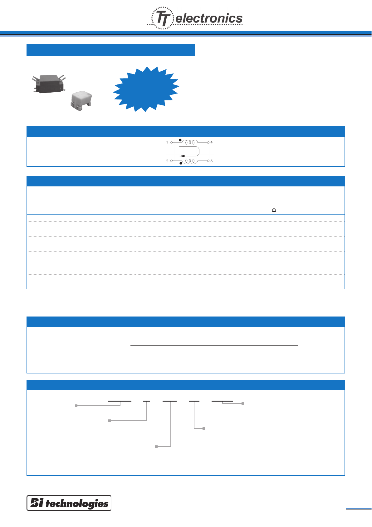
Schematic
• Operating Temperature Range -40°C to +125°C
• Ambient Temperature, Maximum 85°C
• Temperature Rise, Maximum 40°C
• Dielectric Withstanding Voltage 300Vdc
Electrical / Environmental
Surface Mount Common Mode Chokes
Specifications
Notes: (1) Leakage inductance is measured with pin 2 & 3 shorted.
(2) DC resistance is measured at 25°C.
(3) Maximum operating temperature is +85°C.
(4) Common mode inductance & leakage inductance of HM67-10510LF are measured at 100 kHz, 0.05V
Common Mode Inductance Inductance Leakage
@100 kHz - 0.1 V @100 kHz - 0.1 Vrms Rated DCR
(2)
Part (1-4 or 2-3) (1-4)
(1)
Typ. Current Max. Marking Figure
Number Terminals µH µH mA Ω Code
RoHS
Compliant
www.bitechnologies.com
MAGNETIC COMPONENTS SELEC TOR GUIDE 2007/08 EDITION
We reser ve the right to change specif ications without prior notice.
52
Outline Dimensions (Inch / mm)
Figure 1
Outline Dimensions (Inch/mm)
1
2
4
3
Marking Location
Top View
.140
3.55
Max.
Side View
.138
3.5
Max.
Recommended Solder Pad Layout
.40
10.2
.177
4.5
.098
2.5
.047
1.2
Recommended Solder Pad Layout
.067
1.7
.090
2.3
.232
5.9
.087
2.2
Marking
(Refer to Specifications Table)
.37
9.4
Max.
.236
6.0
Max.
Top View
.10±.004
2.5±0.1
Figure 2
Seating Plane
.155
3.9
Max.
Side View
.004/0.10MAX
Bottom View
.138
3.50
Max.
.197
5.00
Max.
.024
0.60
Typ
.

2007/08 EDITION MAGNETIC COMPONENTS SELECTOR GUIDE
We reserve the right to change specif ications without prior notice
www.bitechnologies.com
53
Electrical Characteristies @ 25°C
(A) Attenuation vs. Frequency Graphs
HM67-B110
HM67-S250LF
HM67-B510LF
HM67-B5R0LF
HM67-B110LF

www.bitechnologies.com
MAGNETIC COMPONENTS SELEC TOR GUIDE 2007/08 EDITION
We reser ve the right to change specif ications without prior notice.
54
Electrical Characteristies @ 25°C (Cont’d)
HM67-B222
HM67-S510LF
HM67-B471LF
HM67-B102LF
HM67-B472LF
HM67-B222LF

2007/08 EDITION MAGNETIC COMPONENTS SELECTOR GUIDE
We reserve the right to change specif ications without prior notice
www.bitechnologies.com
55
Electrical Characteristies @ 25°C (Cont’d)
(B) Insertion Loss vs. Frequency Graph
HM67-10510LF
Common Mode
Differential Mode
Insertion Loss (dB)
Frequency (MHz)
Common Mode
Differential Mode
Ambient Temperature (0C)
I
o/p /
I
Rated
(C) Current Derating Curve
HM67-10510LF
 Loading...