


2ch NIM V/F CONVERTER
N2VF-01
(2348 Ver.3)
SER №
APPLICATION OF ELECTRONIC DEVICES
TSUJI ELECTRONICS CO.,LTD
3739 Kandatsu-machi Tsuchiura-city
Ibaraki-Pref 300-0013 Japan
Phone +81-(0)29-832-3031
fax +81-(0)29-832-2662
URL http://www.tsujicon.jp
E-mail info2@tsuji-denshi.co.jp
NIM V-F CONVERTER USER'S MANUAL
Type N2VF-01
A V-F Converter constructed in a NIM-1 UNIT case has two channels outputs and include a four stage
amplification factor switch and a polarity selector switch. In addition, with over range and polarity displayed, V-F
conversion is always performed at the optimum conditions. The over range signal is output as a transistor
open-collector signal which can be used as a warning.
The DC amplifier can be used under isolated floated condition from the NIM power source, providing higher( )
noise tolerance.
1. Specification
1 Gain 1MHz/10V 1MHz/1V 1MHz/100mV, 1MHz/10mV) , ,
) ~ ( ± )2 Input Voltage 0 10V Acceptable input 100V Max
3 Input Resistance 1M or more) Ω
4 Output TTL level or out to 50 by jumper pin positive logic 0 1MHz) ( Ω ) ~
5 Conversion Accuracy 0.02%/FS) <±
) ( )6 Power Supply +6V about 1300mA From NIM Connector
7 Case NIM-1)
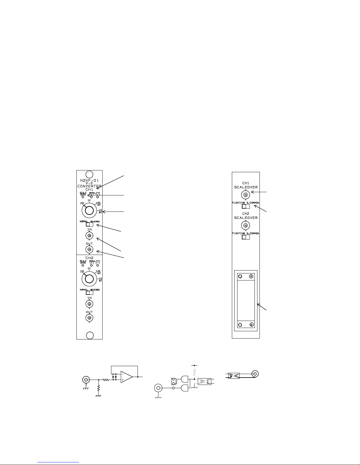
2. Panel lay out
1 Front panel layout 2 Rear panel layout) )
Input polarity lamp
indicate polarity of input voltage
+ lamp on is correct conversion( )
Scale over lamp Scale over output
Lamp on when the input level transistor on when
exceeds conversion level scale over
Input range select SW Floating/Non floating
0~1MHz/0~10V,0~1V,0~100mV, select SW
0~10mV, FLOATING:
Polarity select slide SW input is isolated
If input polarity - , then select G.COMMON:( )
"REVERSE" side input has
Input isolated BNC common GND( )
( )TTL pulse output BNC
GND is common with NIM PWR
NIM connector
NIM BIN Power
Supply
( )+6V 10p
( )0V 34p
3. Circuit of input/output
1 Voltage input 2 Pulse out * 3 Scale over out) ) ( ) )
* Output level exchange TTL 50 is enable by opening( ) ( ←→ Ω)
( )the left side panel and moving jumper pins JP3 for ch1, JP4 for ch2
those are located on the front panel side of the board.
They are set to TTL level side as defaults.
1.5M
Ω
100
kΩ
INPUT
SCALE OVER
+5V
OUTPUT
TTL
50
Ω
JUMPER
 Loading...