

TS9011
250mA CMOS Low Dropout Voltage Regulator
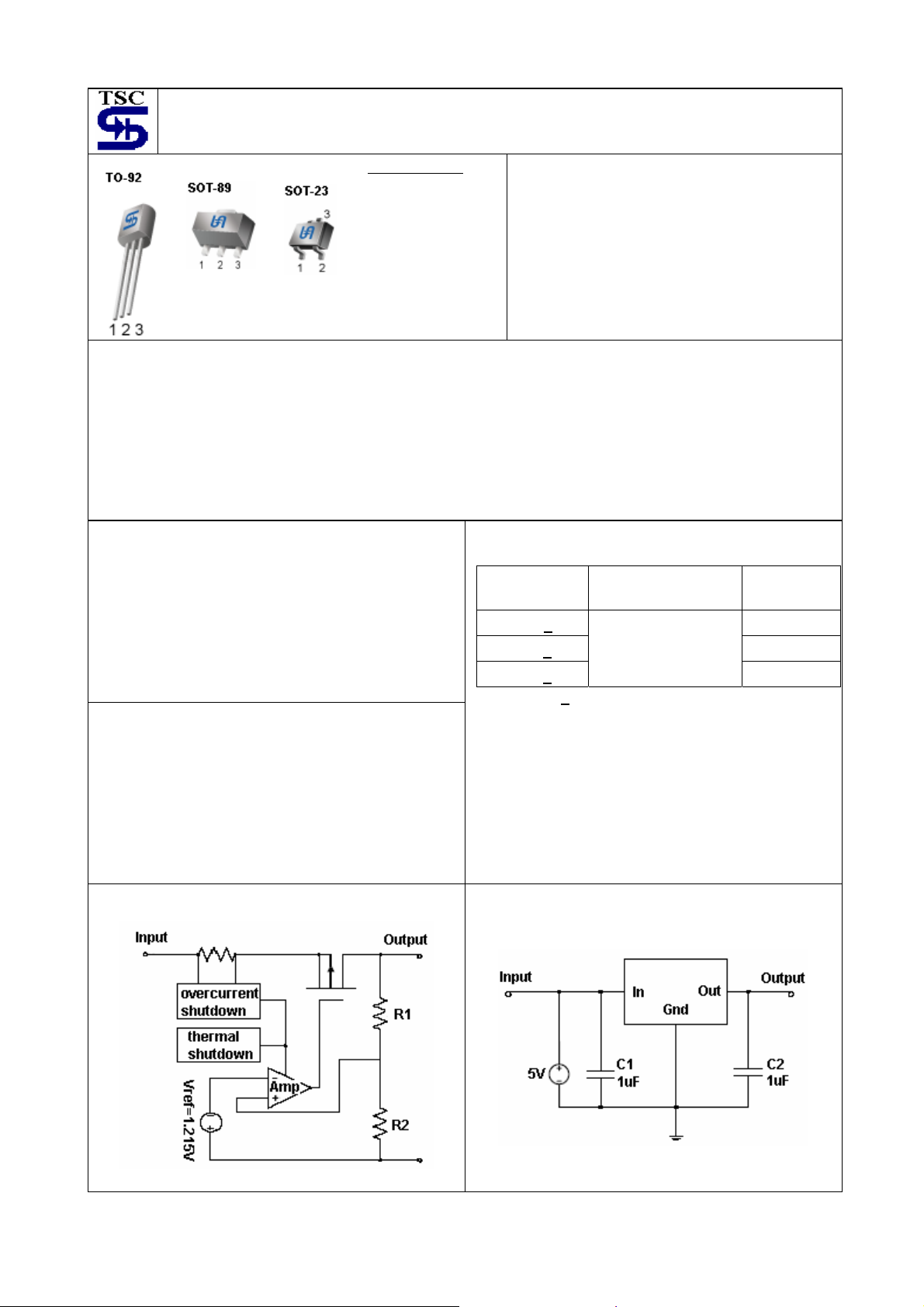
Pin assignment
TO-92 & SOT-89
1. Gnd
2. Input
3. Output
SOT-23
1. Gnd
2. Out
3. Input
Low Power Consumption 2uA
Low Drop Out Voltage 0.4V
General Description
The TS9011 series is a positive voltage regulator developed utilizing CMOS technology featured very low power
consumption, low dropout voltage and high output voltage accuracy. Built in low on-resistor provides low dropout voltage
and large output current. A 1uF or greater can be used as an output capacitor.
The TS9011 series are prevented device failure under the worst operation condition with both thermal shutdown and
current fold-back. These series are recommended for configuring portable devices and large current application,
respectively.
This series are offered in 3-pin TO-92, SOT-89 and SOT-23 package.
Features
Dropout voltage typically 0.38V @Io=200mA (Vo=5V)
Output current up to 250mA
Low power consumption, 2uA(typ) @Vo=5V
Output voltage +/-2%
Internal current limit
Ordering Information
Thermal shutdown protection
Applications
Palmtops
Video recorders
Battery powered equipment
PC peripherals
CD-ROM
Part No.
TS9011xCT TO-92
TS9011xCX SOT-23
TS9011xCY
Note: Where x denotes voltage option, available are
A = 1.5V, D=1.8V, K=2.5V, S=3.3V, 5=5.0V.
Contact factory for additional voltage options.
Operating Temp.
(Ambient)
-20 ~ +85 oC
Package
SOT-89
Digital signal camera
Block Diagram
Typical Application Circuit
TS9011 series 1-4 2003/12 rev. D
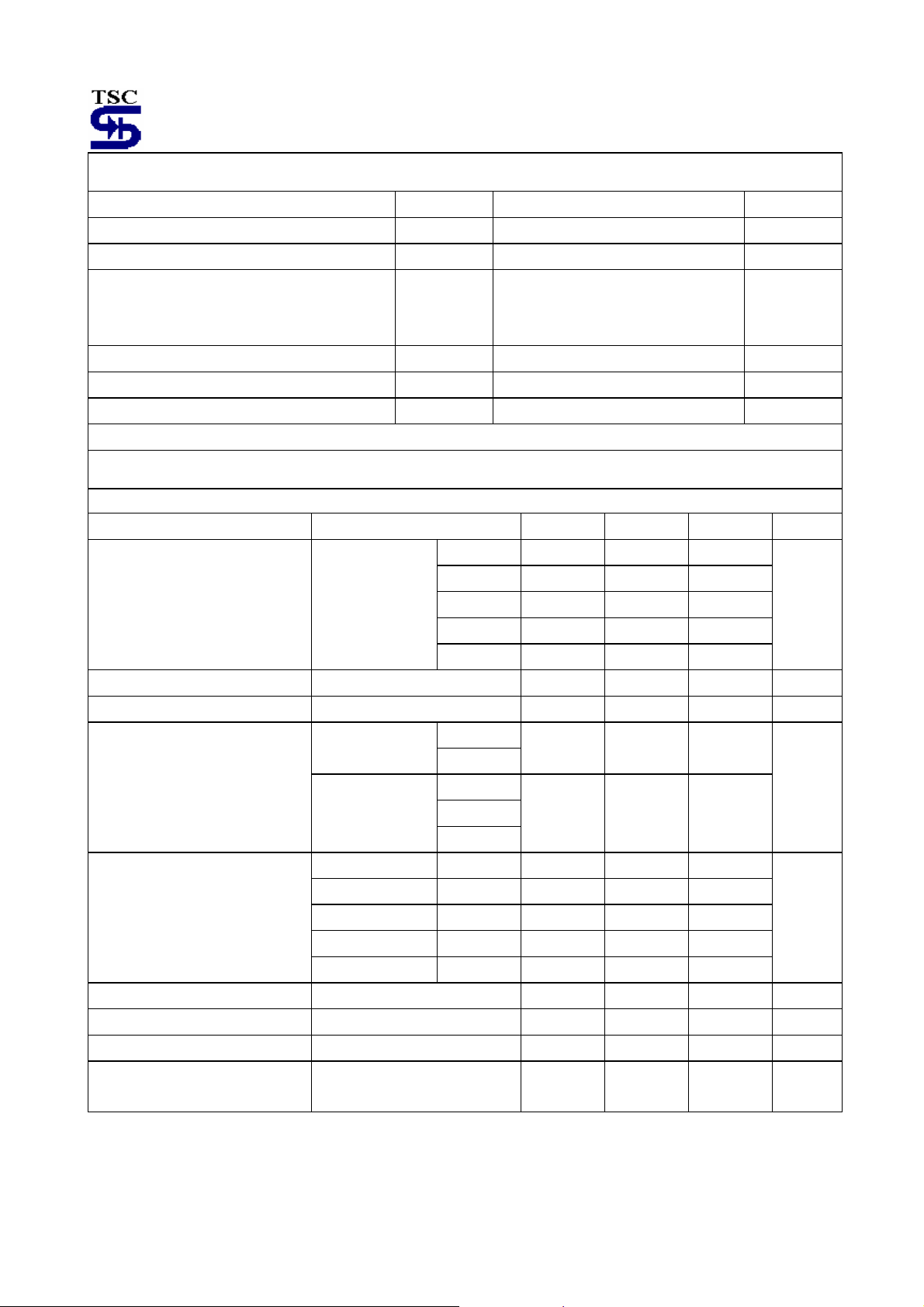
Absolute Maximum Rating
Input Supply Voltage Vin(max.) +12 V
Input Operating Voltage Vin(opr.) +10
Output Current Io PD / (Vin – Vo) V
Power Dissipation SOT-23
SOT-89
TO-92
Operating Junction Temperature Range Tj -40 ~ +125
Storage Temperature Range T
PD 0.15
0.50
0.65
-65 ~ +150
STG
W
o
C
o
C
Lead Soldering Temperature (260 oC) 10 S
Caution: Stress above the listed absolute rating may cause permanent damage to the device.
Electrical Characteristics
Ta = 25 oC unless otherwise specified.
Parameter Conditions Min Typ Max Unit
TS90115 4.900 5.0 5.100
Output Voltage
=40mA,
Maximum Output Current Vin=Vo+1V, 250 -- -- mA
Input Stability Vo+1V ≤ Vin ≤ Vo+2V, Io=1mA -- 0.2 0.3 %
Vin=Vo + 1V, Io
≤100mA
1mA≤I
L
Load Regulation (Note1)
Vin=Vo+1V,
1mA≤IL≤80mA
Io=250mA TS90115 -- 400 600
Io=200mA TS9011S -- 400 650
Dropout Voltage (Note 2)
Io=160mA TS9011K -- 400 700
Io=120mA TS9011D -- 400 750
Io=100mA
Quiescent Current Vin=Vo+1V, Io=0A -- 2 5 uA
Output Current Limit Vout < 0.4V -- 400 -- mA
Power Supply Rejection Ratio At f=100KHz, Io=10mA, -- 30 -- dB
Output Voltage Temperature
Coefficient (Note 3)
Note: 1. Regulation is measured at constant junction temperature, using pulsed ON time.
2. Dropout is measured at constant junction temperature, using pulsed ON time, and the criterion is Vout inside
target value +/-2%.
3. Guaranteed by design.
TS9011S 3.234 3.3 3.366
TS9011K 2.450 2.5 2.550
TS9011D 1.764 1.8 1.836
TS9011A 1.47 1.5 1.53
TS90115 Vin=Vo+1V,
-- 40 80
TS9011S
TS9011K
TS9011D
-- 40 90
TS9011A
TS9011A
-- 850 1000
-- 100 --
V
mV
mV
ppm/ oC
TS9011 series 2-4 2003/12 rev. D
H
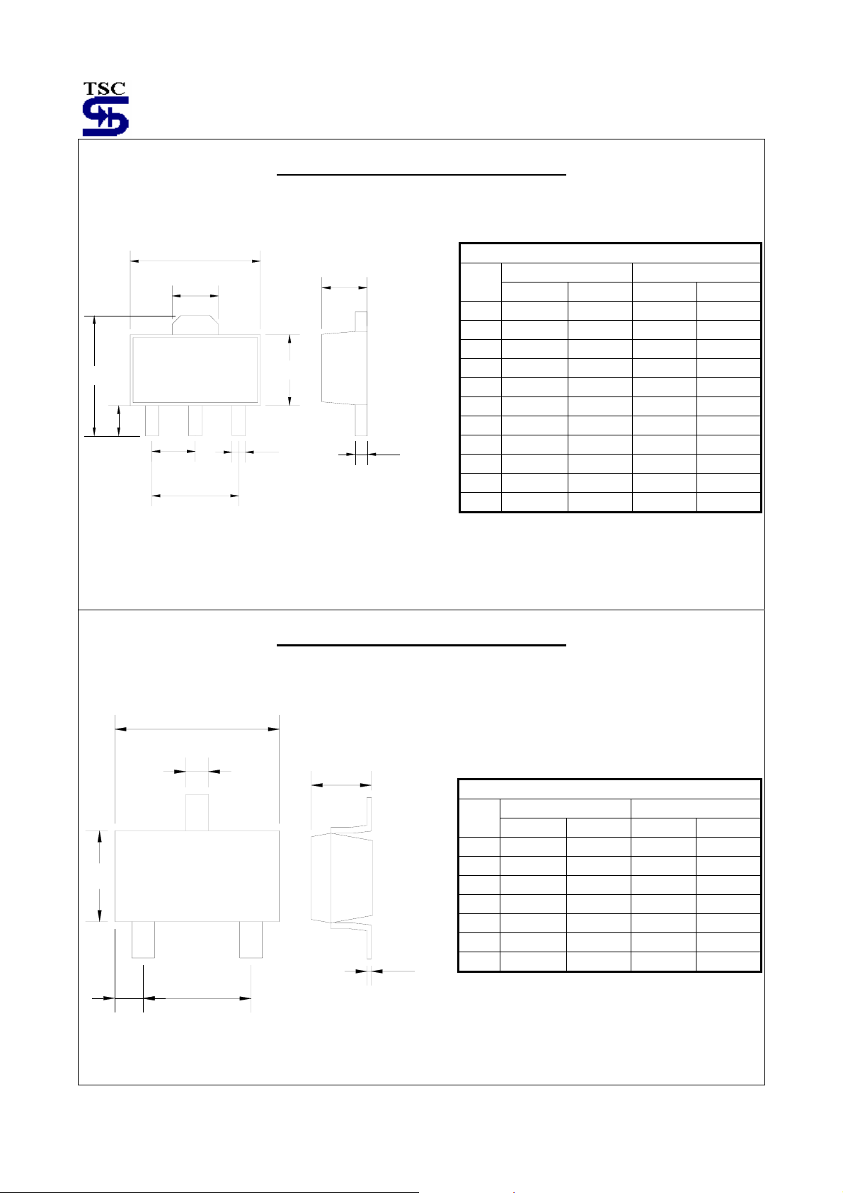
SOT-89 Mechanical Drawing
A
B
G
E
F
D
I
C
J
DIM
A 4.40 4.60 0.173 0.181
B 1.50 1.7 0.059 0.070
C 2.30 2.60 0.090 0.102
D 0.40 0.52 0.016 0.020
E 1.50 1.50 0.059 0.059
F 3.00 3.00 0.118 0.118
G 0.89 1.20 0.035 0.047
H 4.05 4.25 0.159 0.167
I 1.4 1.6 0.055 0.068
J 0.35 0.44 0.014 0.017
SOT-89 DIMENSION
MILLIMETERS INCHES
MIN MAX MIN MAX
SOT-23 Mechanical Drawing
A
B
E
D
C
F
SOT-23 DIMENSION
MILLIMETERS INCHES
MIN MAX MIN MAX
G
DIM
A 2.88 2.91 0.113 0.115
B 0.39 0.42 0.015 0.017
C 1.78 2.03 0.070 0.080
D 0.51 0.61 0.020 0.024
E 1.59 1.66 0.063 0.065
F 1.04 1.08 0.041 0.043
G 0.07 0.09 0.003 0.004
TS9011 series 3-4 2003/12 rev. D
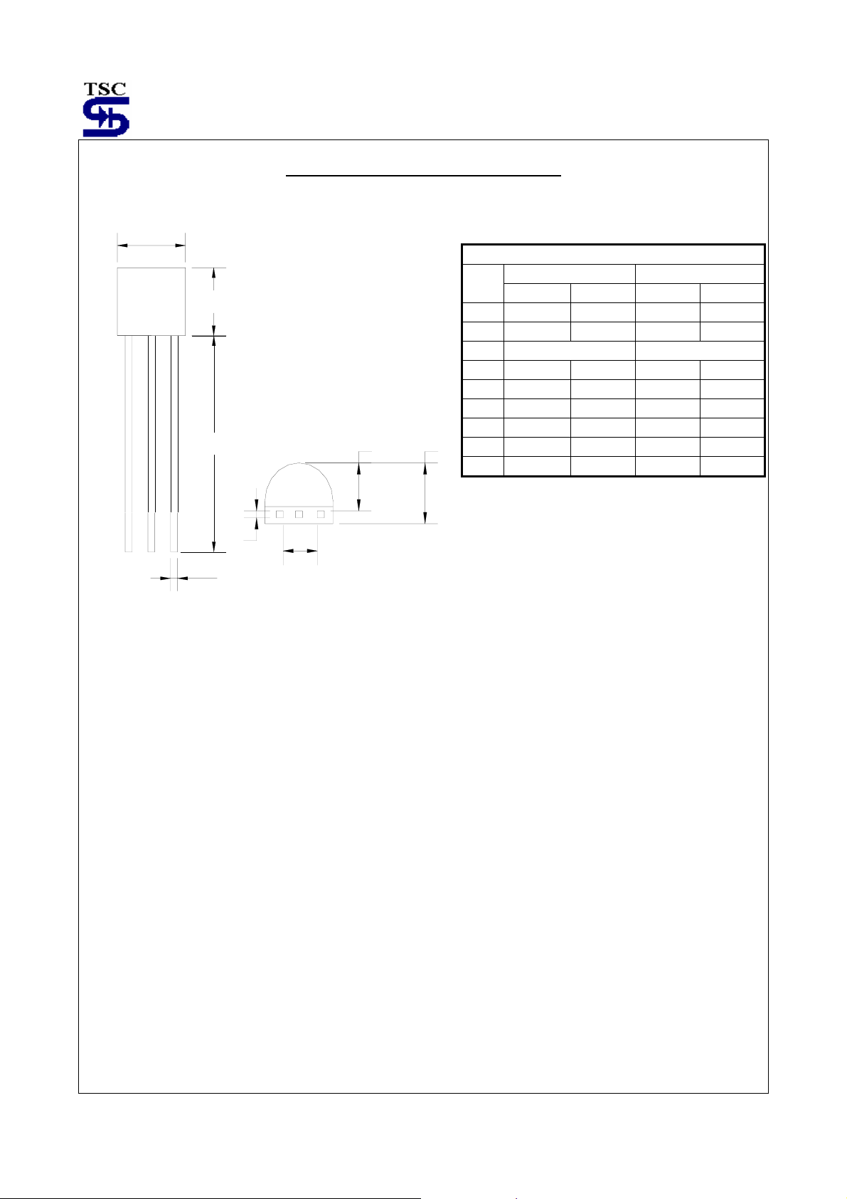
TO-92 Mechanical Drawing
A
TO-92 DIMENSION
DIM
B
C
E F
A 4.30 4.70 0.169 0.185
B 4.30 4.70 0.169 0.185
C 14.30(typ) 0.563(typ)
D 0.43 0.49 0.017 0.019
E 2.19 2.81 0.086 0.111
F 3.30 3.70 0.130 0.146
G 2.42 2.66 0.095 0.105
H 0.37 0.43 0.015 0.017
MILLIMETERS INCHES
MIN MAX MIN MAX
H
D
G
TS9011 series 4-4 2003/12 rev. D
 Loading...