Page 1

查询TS39150CZ05供应商
TS39150
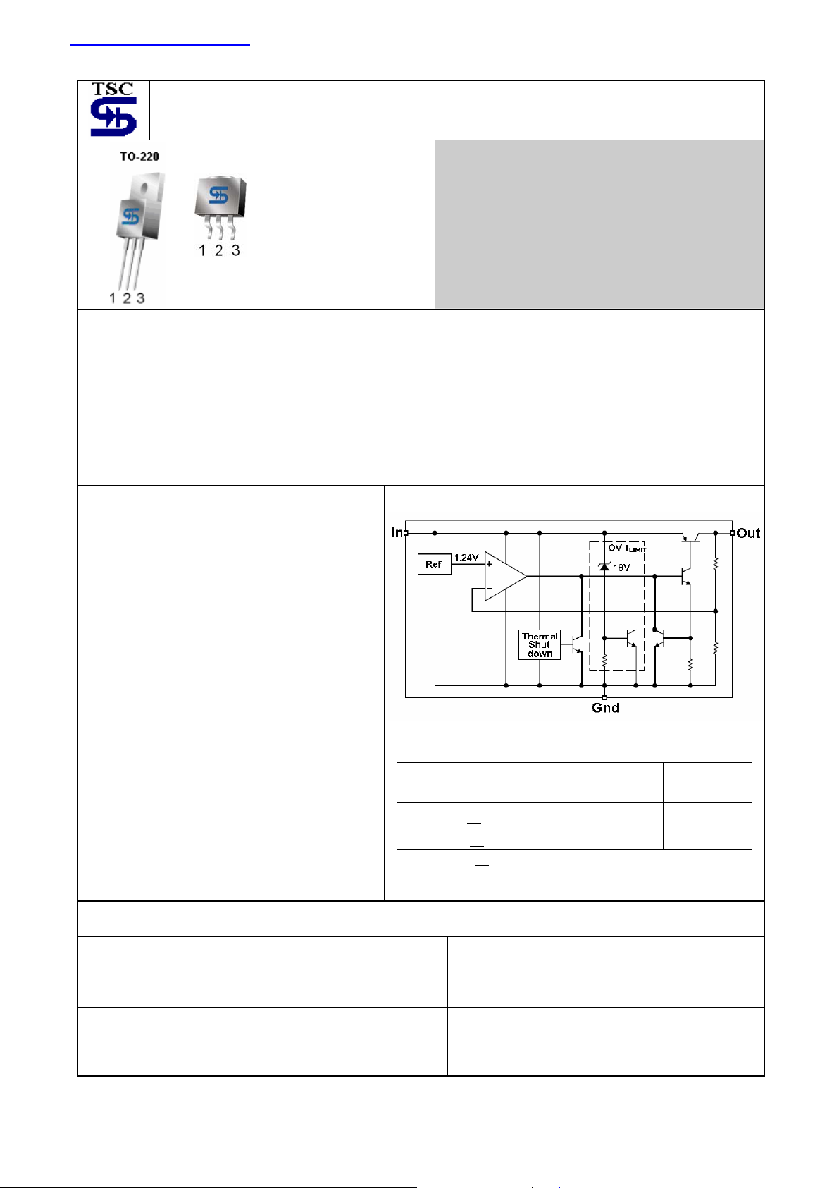
1.5A Ultra Low Dropout Fixed Positive Voltage Regulator
TO-263
Pin assignment:
1. Input
2. Ground
3. Output
Low Dropout Voltage 0.4V (typ.)
General Description
The TS39150 series are using process with a PNP pass element for high current, high accuracy and low dropout voltage
regulators. These regulator s feature 400mV(typ) dropout voltages and very low ground current, these devices also find
applications in lower current and low dropout critical systems, where their tiny dropout voltage and ground current values
are important attributes.
The TS39150 are fully protected against over current faults, reversed input polarity, reversed lead insertion, over
temperature operation, and positive and negative transient voltage spikes.
This series is offered in 3-pin TO-263, TO-220 package.
Features
Dropout voltage typically 0.4V @Io=1.5A
Output current up to 1.5A
Low ground current
Output voltage trimmed before assembly
Extremely fast transient response
+20V Transient peak voltage
-20V Reverse peak voltage
Internal current limit
Block Diagram
Thermal shutdown protection
Applications
Battery power equipment
Automotive electronics
High efficiency “Green” computer system
High efficiency linear power supplies
High efficiency post regulator for switching
supply
Ordering Information
Part No.
TS39150CZxx TO-220
TS39150CMxx
Note: Where xx denotes voltage option, available are 12V, 5.0V,
3.3V and 2.5V. Contact factory for additional voltage
options.
Operation Temp.
(Junction)
-40 ~ +125
o
C
Package
TO-263
Absolute Maximum Rating (Note 1)
Input Supply Voltage (Note 2) Vin -20V ~ +20 V
Operation Input Voltage Vin (operate) 20 V
Power Dissipation (Note 3) PD Internally Limited W
Operating Junction Temperature Range TJ -40 ~ +125
Storage Temperature Range T
Lead Soldering Temperature (260 oC) 5 S
-65 ~ +150
STG
o
C
o
C
TS39150 1-5 2005/3 rev. A
Page 2

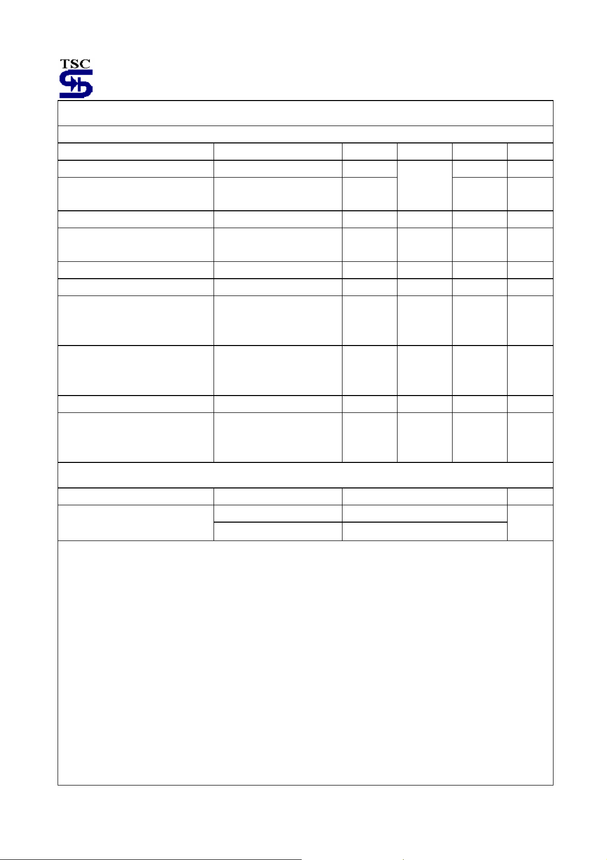
Electrical Characteristics
Vin = Vout + 1V, IL = 10mA, Co = 10uF, Ta = 25
o
C, unless otherwise specified.
Parameter Conditions Min Typ Max Unit
Output Voltage 0.990|Vo| 1.010|Vo| V
Output Voltage 10mA ≤ IL ≤ 1.5A,
Vo+1V ≤ Vin ≤ 26V
Input Supply Voltage -- -- 20 V
Output Voltage Temperature
Coefficient
Line Regulation Vo+1V ≤ Vin ≤ 26V -- 0.05 0.5 %
Load Regulation 10mA ≤ IL ≤ 1.5A -- 0.2 1.0 %
Dropout Voltage (Note 4) IL=100mA
Quiescent Current (Note 5) IL=100uA
Short Circuit Current (Note 6) Vout=0 -- 2.1 3.5 A
Output Noise,
10Hz to 100KHz, IL=100mA
IL=750mA
IL=1.5A
IL=750mA
IL=1.5A
CL=2.2uF
CL=10uF
CL=33uF
0.980|Vo|
-- 40 100 ppm/
--
--
--
--
--
--
--
--
--
12 / 5.0
3.3/ 2.5
80
350
400
100
8
22
600
400
260
1.020|Vo|
200
500
600
--
--
--
--
--
--
V
mV
mA
uVrms
o
C
Thermal Performance
Condition Package type Typ Unit
TO-220 60 Thermal Resistance
Junction to Ambient
Note 1: Absolute Maximum Rating is limits beyond which damage to the device may occur. For guaranteed
Specifications and test conditions see the Electrical Characteristics.
Note 2: Maximum positive supply voltage of 20V must be limited duration (<100mS) and duty cycle (<1%).
Note 3: The maximum allowable power dissipation is a function of the maximum junction temperature, Tj, the junction to
ambient thermal resistance,
dissipation will cause excessive die temperature, and the regulator will go into thermal shutdown. The effective
value of
Note 4: Dropout voltage is defined as the input to output differential at which the output voltage drops 2% below its
nominal value measured at 1V differential.
Note 5: Ground pin current is the regulator quiescent current. The total current drawn from the source is the sum of the
ground pin current and output load current.
Note 6: Output current will decrease with increasing temperature, but it will be not dropped below 1.5A at the maximum
specified temperature.
θja can be reduced by using a heatsink.
TO-263 80
θja, and the ambient temperature , Ta. Exceeding the maximum allowable power
o
C/W
TS39150 2-5 2005/3 rev. A
Page 3

Application Information
Application Information
The TS39150 series are high performance with low
dropout voltage regulator suitable for moderate to high
current and voltage regulator application. Its
400mA(typ) dropout voltage at full load and over
temperature makes it especially valuable in battery
power systems and as high efficiency noise filters in
post regulator applications. Unlike normal NPN
transistor design, where the base to emitter voltage
drop and collector to emitter saturation voltage limit the
minimum dropout voltage, dropout performance of the
PNP output of these devices is limited only by low Vce
saturation voltage.
The TS39150 series is fully protected from damage due
to fault conditions. Linear current limiting is provided.
Output current during overload conditions is constant.
Thermal shutdown the device when the die temperature
exceeds the maximum safe operating temperature.
Transient protection allows device survival even when
the input voltage spikes above and below nominal. The
output structure of these regulators allows voltages in
excess of the desired output voltage to be applied
without reverse current flow.
Typical Application Circuit
Capacitor Requirement
The TS39150 series requires an output capacitor to
maintain stability and improve transient response is
necessary. The value of this capacitor is dependent
upon the output current, lower currents allow smaller
capacitors. TS39150 series regulators are stable with
the 10uF minimum capacitor value at full load. Where
the regulator is powered from a source with high AC
impedance, a 0.1uF capacitor connected between input
and ground is recommended. The capacitor should
have good characteristics to above 250KHz. The
capacitance values will be improved transient response,
ripple rejection and output noise.
Minimum Load Current
The TS39150 series is specified between finite loads.
If the output current is too small leakage currents
dominate and the output voltage rises. A 10mA
minimum load current swamps any expected leakage
current across the operating temperature range.
Thermal Characteristics
TS39150 series linear regulators are simple to use, the
most complicated design parameters to consider are
thermal characteristics, thermal design requires the
following application specification parameters:
z Maximum ambient temperature, Ta
z Output current, Iout
z Output voltage, Vout
z Input voltage, Vin
We calculate the power dissipation of the regulator
from these numbers and the device parameters from
this data sheet. A heatsink may be required depending
on the maximum power dissipation and maximum
ambient temperature of the application. Under all
possible operating conditions, the junction temperature
must be within the range specified under absolute
maximum ratings. To determine if the heatsink is
required, the power dissipated by the regulator, P
must be calculated.
The below formula shows the voltages and currents for
calculating the P
Iin = IL / IG
= (Vin-Vout) * IL + (Vin) * I
P
D
Ex. PD = (3.3V-2.5V) * 1.5A + 3.3V * 11mA
= 1200mW + 36mW
= 1236mW
Remark: IL is output load current,
I
G
Vin is input voltage
Vout is output voltage
The next parameter which must be calculated is the
maximum allowable temperature rise, T
calculated by the using to formula:
(max) = TJ(max) – TA(max)
T
R
Where: T
temperature, which is 125
grade parts.
T
temperature which will be encountered in the
application.
in the regulator:
D
G
is ground current.
(max). this is
R
(max) is the maximum allowable junction
J
(max) is the maximum ambient
A
o
C for commercial
D
TS39150 3-5 2005/3 rev. A
Page 4

Application Information (continues)
Using the calculated values for TR(max) and PD, the
maximum allowable value for the junction to ambient
thermal resistance, θja, can now be found:
θja = T
IMPORTANT: if the maximum allowable value for is
found to be ≥60
o
since the package alone will dissipate enough heat to
satisfy these requirements. If the calculated value for
θja falls below these limits, a heatsink is required.
(max) / P
R
C/W for the TO-263 package, no heatsink is needed
D
o
C/W for the TO-220 package, ≥80
TS39150 4-5 2005/3 rev. A
Page 5

TO-220 Mechanical Drawing
O
K
L
DIM
A 10.000 10.500 0.394 0.413
B 3.240 4.440 0.128 0.175
C 2.440 2.940 0.096 0.116
D - 6.350 - 0.250
E 0.381 1.106 0.015 0.040
F 2.345 2.715 0.092 0.058
M
N
G 4.690 5.430 0.092 0.107
H 12.700 14.732 0.500 0.581
I 8.382 9.017 0.330 0.355
J 14.224 16.510 0.560 0.650
K 3.556 4.826 0.140 0.190
L 0.508 1.397 0.020 0.055
M 27.700 29.620 1.060 1.230
N 2.032 2.921 0.080 0.115
O 0.255 0.610 0.010 0.024
P 5.842 6.858 0.230 0.270
TO-220 DIMENSION
MILLIMETERS INCHES
MIN MAX MIN MAX
A
B
C
P
J
I
D
H
F
E
G
TO-263 Mechanical Drawing
TO-263 DIMENSION
A
E
DIM
F
A 10.000 10.500 0.394 0.413
B 14.605 15.875 0.575 0.625
B
I
H
C
D
G
C 0.508 0.991 0.020 0.039
D 2.420 2.660 0.095 0.105
E 4.064 4.830 0.160 0.190
F 1.118 1.400 0.045 0.055
G 0.450 0.730 0.018 0.029
H 8.280 8.800 0.325 0.346
I 1.140 1.400 0.044 0.055
J 1.480 1.520 0.058 0.060
MILLIMETERS INCHES
MIN MAX MIN MAX
TS39150 5-5 2005/3 rev. A
 Loading...