

查询TS3842供应商
TS3842B/3843B
High Performance Current Mode Controller
Designed for Off-Line and DC-to-DC
converter applications.
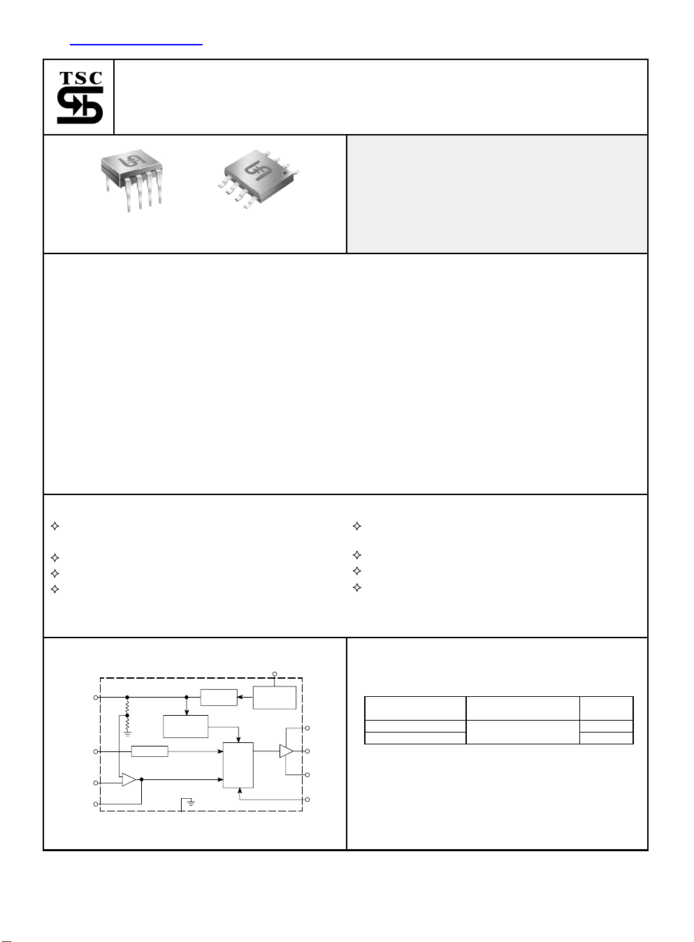
SOP-8DIP-8
General Description
The TS3842B and TS3843B series are high performance fixed frequency current mode controllers.
This is specifically designed for Off-Line and DC-to-DC converter applications offering the designer a
cost effective solution with minimal external components. This integrated circuits feature a trimmed
oscillator for precise duty cycle control, a temperature compensated reference, high gain error
amplifier, current sensing comparator, and a high current totem pole output ideally suited for driving
a power MOSFET.
Also included are protective features consisting of input and reference undervoltage lockouts each
with hysteresis, cycle-by-cycle current limiting, programmable output deadtime, and a latch for
single pulse metering.
This device is available in 8-pin dual-in-line plastic packages as well as the 8-pin plastic surface
mount (SOP-8). The SOP-8 package has separate power and ground pins for the totem pole output
stage.
The TS3842B has UVLO thresholds of 16V (on) and 10V (off), ideally suited for off-line converters.
Features
Trimmed Oscillator Discharge Current for
Precise Duty Cycle Control
Current Mode Operation to 500KHz
Automatic Feed Forward Compensation
Latching PWM for Cycle-By-Cycle Current
Limiting
Internally Trimmed Reference with Undervoltage
Lockout
High Current Totem Pole Output
Undervoltage Lockout with Hystersis
Low Start-Up and Operating Current
Block Diagram Ordering Information
V
7(12)
CC
PWM
V
CC
Undervoltage
Lockout
V
7(11)
Output
6(10)
5(8)
3(5)
C
Power
Ground
Current
Sense
Input
DEVICE
TS3842/3843BCD
TS3842/3843BCS
OPERATING TEMPERATURE
-20 to +85
V
ref
8(14)
R
T/CT
4(7)
Voltage
Feedback
Input
2(3)
Output
Compensation
1(1)
The document contains information on a new product.Specifications and
R
R
Undervoltage
Oscillator
+
-
Error
Amplifier
information herein are subject to change without notice.
V
ref
Lockout
5.0V
Reference
Latching
(Ambient)
PACKAGE
DIP-8
SOP-8
Absolute Maximum Ratings
RATING SYMBOL VALUE UNIT
Total Power Supply and Zener Current (ICC+IZ) 30 mA
Output Current Source or Sink (Note 1) Io 1.0 A
Output Energy (Capacitive Load per Cycle) W 5.0 µJ
Current Sense and Voltage Feedback Inputs Vin -0.3 to +5.5 V
Error Amp Output Sink Current Io 10 mA
Power Dissipation and Thermal Characteristics
Plastic DIP
Maximum Power Dissipation @ T
=25
A
Thermal Resistance Junction to Air
Plastic SOP
Maximum Power Dissipation @ T
Thermal Resistance Junction to Air
=25
A
P
D
θ
JA
R
P
D
θ
JA
R
862
145
1.25
100
Operating Junction Temperature TJ 0 to +150
Operating Ambient Temperature TA -20 to +85
Storage Temperature Range Tstg -25 to +150
mW
/W
W
/W

Electrical Characteristics
VCC=15V (Note 2), RT=10K, CT=3.3nF, TA=T
low
to T
(Note 3), unless otherwise noted.
high
CHARACTERISTIC SYMBOL MIN TYP MAX UNIT
REFFRENCE SECTION
Reference Output Voltage (Io=1.0mA,T
Line Regulation (V
=12V to 25V)
CC
= 25)
J
Vref 4.9 5.0 5.1 V
Regline - 2.0 20 mV
Load Regulation (Io =1.0mA to 20mA) Regload - 3.0 25 mV
Temperature Stability Ts - 0.2 -
Total Output Variation over Line,Load ,and
Temperature
Output Noise Voltage (f = 10Hz to 10kHz, T
Long Term Stability ( T
=125 for 1000 Hours)
A
=25)
J
Vref 4.82 - 5.18 V
Vn - 50 - µV
S-5.0-mV
mV/
Output Short Circuit Current Isc -30 -85 180 mA
OSCILLATOR SECTION
Frequency
T
=25
J
to T
T
A=Tlow
high
Frequency Change with Voltage (V
Frequency Change with Temperature
T
to T
A=Tlow
high
=12V to 25V)
CC
Fosc
fosc/V
fosc/T
47 52 57
46 - 60
-0.21.0%
-5.0-
KHz
%
Oscillator Voltage Swing ( Peak-to-Peak) Vosc - 1.6 - V
Discharge Current (Vosc=2.0V)
T
J
T
A=Tlow
=25
to T
high
Idischg
7.5 8.4 9.3
7.2 - 9.5
mA
Electrical Characteristics
VCC=15V (Note 2), RT=10K, CT=3.3nF, TA=T
low
to T
(Note 3), unless otherwise noted.
high
CHARACTERISTIC SYMBOL MIN TYP MAX UNIT
ERROR AMPLIFIER SECTION
Voltage Feedback Input (Vo=2.5V)
Input Bias Current (V
=5.0V) I
FB
Open-Loop Voltage Gain (Vo=2.0V to 4.0V)
Unity Gain Bandwidth (T
Power Supply Rejection Radio (V
=25)
J
=12V to 25V)
CC
V
FB
IB
A
VOL
2.42 2.5 2.58 V
- -0.1 -2.0
65 90 - dB
a
BW 0.7 1.0 - MHz
PSRR 60 70 - dB
Output Current
Sink (Vo=1.1V, V
Source ( Vo=5.0V, V
=2.7V) I
FB
=2.3V) I
FB
sink
Source
2.0 12 -
-0.5 -1.0 -
mA
Output Voltage Swing
High State (R
Low State (R
=15K to ground, VFB=2.3V) V
L
=15K to Vref, VFB=2.7V) V
L
OH
OL
5.0 6.2 -
-0.81.1
CURRENT SENSE SECTION
Current Sense Input Voltage Gain (Note 4&5) Av 2.85 3.0 3.15 V/V
Maximum Current Sense Input Threshold(Note 4)
Power Supply Rejection Radio
V
=12V to 25V,Note 4
CC
Input Bias Current
Propagation Delay(Current Sense Input to Output)
V
th
0.9 1.0 1.1 V
PSRR - 70 - dB
I
IB
t
PLH(IN/OUT)
- -2.0 -10 µA
-150300ns
A
V

Electrical Characteristics
VCC=15V (Note 2), RT=10K, CT=3.3nF, TA=T
low
to T
(Note 3), unless otherwise noted.
high
CHARACTERISTIC SYMBOL MIN TYP MAX UNIT
OUTPUT SECTION
Output Voltage
Low State (Isink=20mA)
V
OL
-0.10.4
(Isink=200mA) - 1.6 2.2
High State (Isource=20mA)
V
OH
13 13.5 (Isource=200mA) 12 13.4 Output Voltage with UVLO Activated
=6.0V,Isink=1.0mA
V
CC
Output Voltage Rise Time (C
Output Voltage Fall Time (C
=1.0nF,TJ=25)
L
=1.0nF,TJ=25)
L
(UVLO)
V
OL
-0.11.1V
tr - 50 150 ns
tf - 50 150 ns
UNDERVOLTAGE LOCKOUT SECTION
Start-Up Threshold
TS3842B 14.5 16 17.5
Vth V
TS3843B 7.8 8.4 9.0
Minimum Operating Voltage After Turn-On
TS3842B 8.5 10 11.5
V
CC(min)
TS3843B 7.0 7.6 8.2
PWM SECTION
Duty Cycle
Maximum DCmax 94 96 Minimum DCmin - - 0
TOTAL DEVICE
Power Supply Current
Start-Up, V
CC
= 14V
I
CC
- 0.25 0.5
Operating (Note 2) - 12 17
Power Supply Zener Voltage (I
=25mA)
CC
Vz 30 36 - V
V
V
%
mA
Note: 1. Maximum package power dissipation limits must be observed.
2. Adjust V
3. Low duty cycle pulse technique are used during test to maintain junction temperature as close to ambient as possible.
T
4. This parameter is measured at the latch trip point with VFB = 0V.
above the Start-Up threshold before setting to 15V.
CC
= -20 ,T
low
= +85
high
V Output Compensation
5. Comparator gain is defined as : Av =
V Current Sense Input
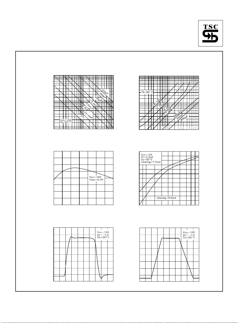
Figure 1 - Timing Resistor vs.
Oscillator Frequency
80
20
Figure 2 - Output Dead Time vs.
Oscillator Frequency
100
50
20
8.0
5.0
RT. TIMING RESISTOR (KΩ)
2.0
0.8
10K 20K 50K
fosc, OSCILLATOR FREQUENCY (KHz)
100K 200K 500K 1.0M
Figure 3 - Oscillator Discharge
Current vs. Temperature
9.0
8.5
8.0
7.5
Idischg. DISCHARGE CURRENT (mA)
7.0
T
. AMBIENT TEMPERATURE (oC)
A
75 100 12550250-25-55
Figure 5 - Error Amp Small
Signal Transient Response
20
10
5.0
2.0
% DT. PERCENT OUTPUT DEAD-TIME
1.0
10K 20K 50K
fosc, OSCILLATOR FREQUENCY (KHz)
100K 200K 500K 1.0M
Figure 4 - Maximum Output Duty
Cycle vs. Timing Resistor
100
90
80
70
60
50
Dmax. MAXIMUM OUTPUT DUTY CYCLE (%)
40
800 1.0K 2.0K 3.0K 4.0K 6.0K 8.0K
RT. TIMING RESISTOR (Ω)
Figure 6 - Error Amp Large
Signal Transient Response
2.55V
2.5V
2.45V
0.15µs/DIV
20mV/DIV
3.0V
2.0V
2.5V
200mA/DIV
10µs/DIV
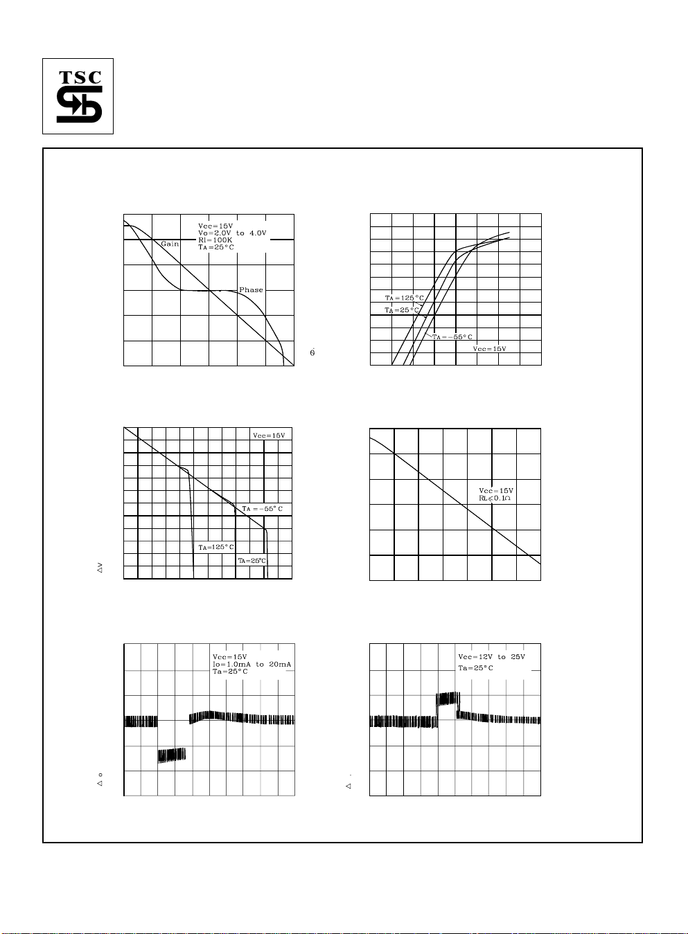
Figure 7 - Error Amp Open-Loop
Gain and Phase vs. Frequency
100
Figure 8 - Current Sense Input Thresh-
0
old vs. Error Amp Output voltage
1.2
80
60
40
20
0
Avol.OPEN-LOOP VOLTAGE GAIN (dB)
-20
10 100
10K 100K 1.0M 10M
1.0K
f. FREQUENCY (Hz)
Figure 9 - Reference Voltage
Change vs. Source Current
0
-4.0
-8.0
-12
-16
-20
Vref. REFERENCE VOLTAGE CHANGE (mV)
r
-24
0 20 40 60 80 100 120
Iref.REFERENCE SOURCE CURRENT (mA)
Figure 11 - Reference Load
Regulation
30
60
90
120
150
EXCESS PHASE (DEGREES)
180
1.0
0.8
0.6
0.4
0.2
Vth. CURRENT SENSE INPUT THRESHOLD (V)
0
0 2.0 4.0 6.0 8.0
Vo. ERROR OUTPUT VOLTAGE (Vo)
Figure 10 - Reference Short Circuit
Current vs. Temperature
110
90
70
Isc. REFERENCE CIRCUIT CURRENT (mA)
50
0-25-55 5025 75 100 125
TA. AMBIENT TEMPERATURE (oC)
Figure 12 - Reference Line
Regulation
Vo.OUTPUT VOLTAGE CHANGE (2.0mV/DIV)
r
2.0ms/DIV
Vo.OUTPUT VOLTAGE CHANGE (2.0mV/DIV)
r
2.0ms/DIV

Figure 13 - Output Saturation
Voltage vs. Load Current
0
-1.0
-2.0
3.0
2.0
1.0
Vsat. OUTPUT SATURATION VOLTAGE (V)
0
0 200 400 600 800
Io. OUTPUT LOAD CURRENT (mA)
Figure 15 - Output Cross
Conduction
Figure 14 - Output Waveform
90%
10%
50ns / DIV
Figure 16 - Supply Current vs.
Supply Voltage
25
Vo. OUTPUT VOLTAGE
Icc. SUPPLY CURRENT
50ns / DIV
20V / DIV
100mA / DIV
20
15
10
5
Icc. SUPPLY CURRENT (mA)
0
010203040
Vcc. SUPPLY VOLTAGE (V)

Figure 17- Representative Block Diagram
V
ref
8(14)
R
T
4(7)
C
T
Voltage
Feedback
Input
2(3)
Output/
Compensation
1(1)
Pin numbers adjacent to terminals are for the 8-pin dual-in-line package.
Pin numbers in parenthesis are for the D suffix SOP-14 package.
2.5V
R
R
Error
Amplifier
Internal
Bias
Oscillator
+
1.0mA
2R
Gnd
R
Reference
Regulator
3.6V
1.0V
Current Sense
Comparator
5(9)
+
-
Figure 18 - Timing Diagram
V
ref
UVLO
S
R
V
CC
UVLO
Q
V
PWM
Latch
V
CC
CC
7(12)
V
in
36V
(See
+
Text)
-
V
C
7(11)
Output
Q1
6(10)
Power Ground
5(8)
Current Sense Input
3(5)
R
S
= Sink Only Positive True Logic
Capacitor C
Latch
"Set" Input
Output/
Compensation
Current Sense
Input
Latch
"Reset" Input
Output
T
Large RT/Small C
T
Small RT/Large C
T

Undervoltage Lockout
Two undervoltage lockout comparators have been incorporated to guarantee that the IC is fully
functional before the output stage is enabled. The positive power supply terminal (Vcc) and the
reference output (Vref) are each monitored by separate comparators. Each has built-in hysteresis
to prevent erratic output behavior as their respective thresholds are crossed. The large hysteresis
and low start-up current of the TS3842B makes it ideally suited in off-line converter applications
where efficient bootstrap start-up technique (Figure 33). 36V zener is connected as a shunt
regulator from Vcc
occur during system start-up. The minimum operating voltage for the TS3842B is 11 V.
Output
These devices contain a single totem pole output stage that was specifically designed for direct
drive of power MOSFET’s. It is capable of up to ±1.0A peak drive current and has a typical rise and
fall time of 50 ns with a 1.0nF load. Additional internal circuitry has been added to keep the output
in a sinking mode whenever an undervoltage lockout is active. This characteristic eliminates the
need for an external pull-down resistor.
The SOP-8 surface mount package provides separate pins for Vc(output supply) and Power Ground.
Proper implementation will significantly reduce the level of switching transient noise imposed on
the control circuitry. This becomes particularly useful when reducing the Ipk(max) clamp level.
The separate Vc supply input allows the designer added flexibility in tailling the drive voltage
independent of Vcc. A zener clamp is typically connected to this input when driving power MOSFET s
in systems where Vcc is greater than 20V. Figure 25 shows proper power and control ground
connections in a current sensing power MOSFET application.
to ground. Its purpose is to protect the IC from excessive voltage that can
Reference
The 5.0V bandgap reference is trimmed to ±2.0% on the TS3842B. Its primary purpose to supply
charging current to the oscillator timing capacitor. The reference has short circuit protection and
is capable of providing in excess of 20mA for powering additional control system circuitry.
Design Considerations
Do not attempt to construct the converter on wire wrap or plug-in prototype boards.
High frequency circuit layout techniques are imperative to prevent pulsewidth jitter. This is usually
caused by excessive noise pick-up imposed on the Current Sense or Voltage Feedback inputs.
Noise immunity can be improved by lowering circuit impedances at these points. The printed
circuit layout should contain a ground plane with low-current signal and high-current switch and
output grounds returning separate paths back to the input filter capacitor. Ceramic bypass capacitors
(0.1µF) connected directly to Vcc,Vc, and Vref may be required depending upon circuit layout.

Undervoltage Lockout(contd.)
This provides a low impedance path for filtering the high frequency noised. All high current loops
should be kept as short as possible using heavy copper runs to minimize radiated EMI. The Error
Amp compensation circuitry and the converter output voltage divider should be located close to
the IC and as far as possible from the power switch and other noise generating components.
Figure 19 - Continuous Current Waveforms
(A)
∆
1
Control Voltage
Inductor
Current
Control Voltage
t
0
t
4
m
m
1
m
11
+
∆∆
m
Oscillator Period
m
1
Oscillator Period
2
2
1
t1t
(B)
m
3
+
∆∆
11
2
m
2
t
5
m
m
2
2
m
m
1
1
t
3
Inductor
Current
t
6
Current mode converters can exhibit subharmonic oscillations when operating at a duty cycle
greater than 50% with continuous inductor current. This instability is independent of the regulators closed loop characteristics and is caused by the simultaneous operating conditions of fixed
frequency and peak current detecting. Figure 19(A) shows the phenomenon graphically. At t
switch conduction begins causing the inductor current to rise at a slope of m
. This slope is a
1
function of the input voltage divided by the inductance. At t1, the Current Sense Input reaches the
threshold established by the control voltage. This causes the switch to turn off and the current to
decay at a slope of m
perturbation is added to the control voltage, resulting in a small
, until the next oscillator cycle. This unstable condition can be shown if a
2
1(dashed line). With a fixed
oscillator period, the current decay time is reduced, and the minimum current at switch turn-on(t
is increased by
1m
)(m2/m1). This perturbation is multiplied by m2/m1 on each succeeding cycle, alternately
2/m1
1+
1m
. The minimum current at the next cycle (t3) decreases to (
2/m1
1+
increasing and decreasing the inductor current at switch turn-on. Several oscillator cycles may be
required before the inductor current reaches zero causing the process to commence again. If m
is greater than 1, the converter will be unstable. Figure 19(B) shows that by adding an artificial
m
1
ramp that is synchronized with the PWM clock to the control voltage, the
decrease to zero on succeeding cycles. This compensating ramp (m
or slightly greater than m
/2 for stability. With m2/2 slope compensation, the average inductor
2
) must have a slope equal to
3
1 perturbation will
current follows the control voltage yielding true current mode operation. The compensating ramp
can be derived from the oscillator and added to either the Voltage Feedback or Current Sense
inputs (Figure 32).
,
0
)
2
/
2

Undervoltage Lockout(contd.)
Figure 20 - External Clock
Synchronization
V
ref
8(14)
R
R
T
External
Sync
Input
0.01
The diode clamp is required if the Sync amplitude is large enough to
cause the bottom side of C
4(7)
C
T
2(3)
4
1(1)
to go more than 300mV below ground.
T
Bias
R
Osc
+
2R
R
EA
5(9)
Firuge 22-Adjustable Reduction
of Clamp Level
V
ref
8(14)
R
R
4(7)
R
2
EA
2(3)
1(1)
R
1
+
I
pk(max)
V
Bias
Osc
1.0 mA
Clamp
5.0V Ref
+
-
V
Clamp
S
Q
2R
=
=
R
R
Comp/Latch
1.0V
5(9)
V
Clamp
Where: 0 V
1.0 V
ɷɷ
R
S
1.67
R
2
+
(
R
1
Clamp
R1R
-3
2
(
+
R1 R
2
+ 0.33x10
1
)
V
V
CC
7(12)
in
+
7(11)
Q1
6(10)
5(8)
3(5)
R
S
)
Figure 24- Adjustable Buffered Reduc-
tion of Clamp Level with Soft-Start
8(14)
1.0M
C
R
Bias
R
4(7)
2(3)
1(1)
Osc
+
1.0mA
EA
5.0V Ref
+
-
2R
R
5(9)
S
Q
R
1.0V
Figure 21 - External Duty Cycle Clamp
and Multi Unit Synchronization
8(14)
4(7)
2(3)
1(1)
B
To Additional
TS384X's
R
Bias
R
Osc
+
2R
EA
R
5(9)
R
A
8 4
R
B
6
5
2
C
f
=
(RA R
5.0k
5.0k
5.0k
1
1.44
)
B
3
R
Q
7
S
R
B
D
=
max
++
RA 2R
Figure 23- Soft-Start Circuit
5.0V Ref
+
-
2R
R
5(9)
S
Q
R
1.0V
C
I
Soft-Start
8(14)
4(7)
2(3)
1.0M
1(1)
=3600c in µF
R
Bias
R
Osc
+
1.0mA
EA
Figure 25- Current Sensing Power MOSFET
V
V
CC
in
RSI
pk xrDS(on)
V
(12)
5.0V Ref
+
-
S
Q
R
Comp/Latch
Control Circuitry Ground:
To pin (9)
Virtually lossless current sensing can be achieved with the implementation of a SENSEFET power switch. For proper operation
during over current conditions, a reduction of the Ipk(max) clamp
level must be implemented. Refer to Figure 22 and 24.
Rs
+
-
(11)
G
(10)
(8)
(5)
R
1/4 W
pin 5
If: SENSEFET = MTP10N10M
R
S
Then: V
D
SENSEFET
S
K
M
Power Ground:
To Input Source
S
= 200
=
pin 5
Return
r
DM(on)RS
=
0.075 I
+
pk

Undervoltage Lockout(contd.)
Figure 26- Current Waveform Spike Suppression Figure 27- MOSFET Parasitic Oscillations
5.0V Ref
+
-
S
R
Comp/Latch
The addition of RC filter will eliminate instability caused
by the leading edge spike on the current waveform.
Figure 28- Bipolar Transistor Drive
I
B
+
0
-
The totem-pole output can finish negative base current for enhanced transistor turn-off with the additions of capacitor C1.
Base Charge
Removal
V
7(12)
+
-
Q
V
CC
7(11)
6(10)
5(8)
3(5)
in
5.0V Ref
+
Q1
R
C
R
S
-
S
R
Comp/Latch
Figure 29- Isolated MOSFET Drive
V
in
5.0V Ref
+
-
S
Q
R
Comp/Latch
6(10)
5(8)
3(5)
C1
Q1
R
S
V
CC
7(12)
+
-
Q
V
CC
7(12)
+
-
7(11)
6(10)
5(8)
3(5)
C
7(11)
6(10)
5(8)
3(5)
Isolation
Boundary
R
R
V
in
R
g
Q1
R
S
V
in
VGS Waveforms
+
0
50% DC 25% DC
V
(pin1)
Ipk
=
3 R
N
P
+
0
-
_
1.4
N
S
(
N
p
S
Q1
N
S
S
Figure 30- Latched Shutdown
)
8(14)
R
Bias
R
4(7)
2(3)
3905
1(1)
2N
2N
3903
MCR
101
The MCR101 SCR must selected for a holding of less than 0.5mA at
(min.). The simple two transistor circuit can be used in place of the
T
A
SCR as shown. All resistors are 10k.
Osc
+
1.0 mA
2R
EA
R
5(9)

Undervoltage Lockout(contd.)
Figure 31-Error Amplifier Compensation
From V
O
R
i
C
f
R
d
Error Amp compensation circuit for stabilizing any current mode topology except for boost and flyback
converters operating with continuous inductor current.
From V
O
R
p
R
i
C
p
C
f
R
d
Figure 32-Slope Compenstaion
MPS3904
R
From V
slope
O
R
R
C
i
C
d
2.5V
+
1.0mA
2(3)
R
f
1(1)
2(3)
R
f
1(1)
EA
2.5V
EA
8(14)
R
T
4(7)
T
2(3)
f
R
1(1)
EA
f
-3.0m
2R
R
5(9)
+
1.0mA
2R
R
5(9)
+
-
5.0V Ref
R
Bias
R
Osc
+
1.0mA
2R
-m
S
Q
R
1.0V
R
Comp/Latch
m
5(9)
V
CC
7(12)
V
in
36V
+
-
7(11)
Q1
6(10)
5(8)
3(5)
R
S
The buffered oscillator ramp can resistively summed with either the voltage feedback or current sense inputs to provide slope compensation.

Undervoltage Lockout(contd.)
Figure 33-27 Watt Off-Line Regulation
W
4.7
MDR
115 Vac
Vref
8(14)
0.01
10k
4(7)
4700pF
18k
4.7k
2(3)
100
150k
pF
1(1)
202
R
Bias
R
Osc
+
EA
1.0mA
2R
+
250
56k
7(12)
5.0V Ref
+
-
+
-
S
Q
R
1.0V
Comp/Latch
R
5(9)
7(11)
6(10)
5(8)
3(5)
4.7k
+
1N4935 1N4935
68
++
100
1N4937
22
1.0k
470pF
L1
MBR1635
T1
3300
2200
pF
MUR110
1000
47
1000
MUR110
680pF
2.7k
MTP
4N50
0.5
5.0V/4.0A
++
1000
5.0V RTN
12V/0.3A
L2
++
10
+
12V RTN
-
10
++
-12V/0.3A
L3
1N4937
TEST CONDITIONS RESULTS
Line Regulation: 5.0V
±12V
Vin=95 to 130 Vac
Load Regulation: 5.0V Vin=115Vac, Iout =1.0A to 4.0A
±12V Vin=115Vac,Iout=100mA to 300mA
Output Ripple: 5.0V 40mVp-p
±12V 80 Vp-p
Vin=115Vac
=50mV or ±0.5%
=24mV or ±0.1%
=300mV or ±3.0%
=60mV or ±0.25%
Efficiency Vin=115Vac 70%
All outputs are at nominal load currents unless otherwise noted.
T1
Primary : 45 Turns #26 AWG
Secondary ±12V :
9 Turns #30 AWG (2 strands )
Bifiliar Wound.
Secondary 5.0V :
4 Turns (six strands) #26
Hexfiliar Wound.
Secondary Feedback :
10 Turns #30 AWG (2 strands)
Bifiliar Wound.
Core :
Ferroxcube EC35-3C8
Bobbin :
Ferroxcube EC35PCB1
Gap :
≅@0.10” for a primary induc-
tance of 1.0mH.
L1:
µH at 5.0A, Coilcraft 27156.
15
L2,L3:
µH at 1.0A, Coilcraft 27157.
25

Undervoltage Lockout(contd.)
Figure 34-33 Watt Off-Line Flyback Converter with Soft-Start and Primary Power Limiting
3 each
0.0047 UL / CSA
1.0A
15
T
Cold
Optional R.F.I Filter
1N4003
3/200
Vac
1N4742
1N4001
180/
200V
Pout Pout
5.0K
7.5K
25K
2.2M
0.01
0.01
1N4687
33K
8.2K
1.5K
22K
6.8K
27K
47 / 25V
10
1
2
3
Comp
14
PJ34060
13
Vref
12
D
T
10
4
0.001
11K
1N4148
9
Vcc
C
8
E
7
Gnd
T
C
R
T
200
65
47K
2.7K
TEST CONDITIONS RESULTS
Line Regulation 5.0V Vin=95 to 135 Vac, Io=3.0A 20mV 0.40%
Line Regulation± 12V Vin=95 to 135 Vac, Io=±0.75A 52mV 0.26%
Line Regulation 5.0V Vin=115 Vac, Io=1.0 to 4.0A 476mV 9.5%
Line Regulation± 12V Vin=115 Vac, Io=±0.4 to ±0.9A 300mV 2.5%
Line Regulation 5.0V Vin=115 Vac, Io=3.0A 45 mVp-p P.A.R.D.
Line Regulation± 12V Vin=115 Vac, Io=±0.75A 75 mV p-p P.A.R.D.
Efficiency 74%
Vin=115 Vac, Io(5.0V)=3.0A
Io(±12V)=±0.75A
L1
MJE
13005
1N5824
100
2200
/10V
/10V
1N4934
1000
/25V
1000
/25V
1N4934
1.0
10
/35V
L3
L2
10
/35V
1N4934
MPS
A05
10/25V
MPS
A55
47
T1
Coilcraft 11-464-16, 0.025” gap
in each leg
Bobbin :
Coilcraft 37-573
Windings:
Primary, 2 each:
75 turns #26 Awg Bifilar wound
Feedback:
15 turns #26 Awg
Secondary , 5.0V:
6 turns #22 Awg Bifilar wound
Secondary , 5.0V:
14 turns #24 Awg Bifilar wound
L1
Coilcraft Z7156. 15
µF @ 5.0A
5.0V /3.0A
12V /0.75A
Common
12V /0.75A
L2,L3
Coilcraft
Z7157. 25µF @ 1.0A

Pin Function Description
PIN NO. FUNCTION DESCRIPTION
1 Compensation
2 Voltage Feedback
3 Current Sense
4
R
T/CT
This pin is the Error Amplifier output and is made available
for loop compensation
This is the inverting input of the Error Amplifier. It is normally
connected to the switching power supply output through a
resistor divider.
A voltage proportional to inductor current is connected to this
input. The PWM uses this information to terminate the output
switch conduction.
The Oscillator Frequency and maximum Output duty are
programmed by connecting resistor R
to ground operation to 500kHz is possible
C
T
to Vref and capacitor
T
5Gnd
6Output
This pin is the combined control circuitry and power ground
(8-pin package only).
This output directly drives the gate of a power MOSFET.
Peak current up to 1.0A are sourced and sunk by this pin.
7 Vcc This pin is the positive supply of the control IC.
8Vref
This pin is the reference output. It provides charging current
for capacitor C
through resistor RT.
T
DIP-8 SOP-8
58
41
PIN : 1. Compensation
2. Voltage feedback
3. Current Sense
4. RT / C
T
5. Gnd
6. Output
7. V
CC
8. V
ref
1
58
4

Operating Description
The TS3842B series are high performance, fixed frequency, current mode controllers. They are
specifically designed for Off-Line and DC-to-DC converter applications offering the designer a cost
effective solution with minimal external components. A representative block diagram is shown in
Figure 17.
Oscillator
The oscillator frequency is programmed by the values selected for the timing components RT and
. Capacitor CT is charged from the 5.0V reference through resistor RT to approximately 2.8V
C
T
and discharge to 1.2V by an internal current sink. During the discharge of C
generates an internal blanking pulse that holds the center input of the NOR gate high. This
causes the Output to be in a low state, thus producing a controlled amount of output deadtime.
Figure 1 shows R
Frequency, both for given values of C
versus Oscillator Frequency and Figure 2, Output Deadtime versus Oscillator
T
. Note that many values of RT and C
T
oscillator frequency but only one combination will yield a specific output deadtime at a given
frequency. The oscillator thresholds are temperature compensated, and the discharge current is
=25
trimmed and guaranteed to within ±10% at T
. These internal circuit refines minimum
J
variations of oscillator frequency and maximum output duty cycle. The results are shown in Figure
3 and 4.
In many noise sensitive applications it may be desirable to frequency-lock the converter to an
external system clock. This can be accomplished by applying a clock signal to the circuit shown
in Figure 20 for reliable locking. The free-running oscillator frequency should be set about 10%
less than the clock frequency. A method for multi unit synchronization is shown in Figure 21. By
tailling the clock waveform, accurate Output duty cycle clamping can be achieved.
, the oscillator
T
will give the same
T
Error Amplifier
A fully compensated Error Amplifier with access to the inverting input and output is provided. It
features a typical DC voltage gain of 90dB, and a unity gain bandwidth of 1.0MHz with 57 degrees
of phase margin (Figure 7). The non-inverting input is internally biased at 2.5V and is not pinned
out. The converter output voltage is typically divided down and monitored by the inverting input.
The maximum input bias current is -2.0µA which can cause an output voltage error that is equal
to the product of the input bias current and the equivalent input divider source resistance.
The Error Amp Output (Pin 1) is provided for external loop compensation (Figure 31). The output
voltage is offset by two diode drops (
input of the Current Sense Comparator. This guarantees that no drive pulses appear at the Output
(Pin 6) when Pin 1 is at its lowest state (V
≈≈
≈1.4V) and divided by three before it connects to the inverting
≈≈
). This occurs when the power supply is operating and
OL

the load is removed, or at the beginning of a soft-start interval (Figure 23,24). The Error Amp
minimum feedback resistance is limited by the amplifier’s source current (0.5mA) and the required output voltage (V
R
= [3x(1.0V)+1.4V] / 0.5mA = 8800Ω
f(MIN)
) to reach the comparator’s 1.0V clamp level:
OH
Current Sense Comparator and PWM Latch
The TS3842B operate as a current mode controller, whereby output switch conduction is initiated
by the oscillator and terminated when the peak inductor current reaches the threshold level established by the Error Amplifier Output/Compensation (Pin 1). Thus the error signal controls the peak
inductor current on a cycle-by-cycle basis. The Current Sense Comparator PWM Latch configuration used ensures that only a single appears at the Output during any given oscillator cycle. The
inductor current is converted to a voltage by inserting the ground referenced sense resistor R
series with the source of output switch Q1. This voltage is monitored by the Current Sense Input
(Pin 3) and compared to a level derived from the Error Amp Output. The peak inductor current
under normal operating conditions is controlled by the voltage at pin 1 where:
in
S
I
= [V(Pin 1) - 1.4V] / 3R
PK
S
Abnormal operating conditions occur when the power supply output is overloaded or if output
voltage sensing is lost. Under these conditions, the Current Sense Comparator threshold will be
internally clamped to 1.0V. Therefore the maximum peak switch current is:
I
PK (MAX)
= 1.0V / R
S
When designing a high power switching regulator it becomes desirable to reduce the internal
clamp voltage in order to keep the power dissipation of R
to a reasonable level. A simple method
S
to adjust this voltage is shown in Figure 22. The two external diodes are used to compensate the
internal diodes yielding a constant clamp voltage over temperature. Erratic operation due to noise
pickup can result if there is an excessive reduction of the I
(max) clamp voltage.
PK
A narrow spike on the leading edge of the current waveform can usually be observed and may
cause the power supply to exhibit an instability when the output is lightly loaded. This spike is
due to the power transformer interwinding capacitance and output rectifier recovery time. The
addition of an RC filter on the Current Sense Input with a time constant that approximates the
spike duration will usually eliminate the instability: refer to Figure 26.

58
14
A
C
D
G
DIP-8
B
K
SYMBOLS
MILLIMETERS INCHES
MIN MAX MIN MAX
A 9.07 9.32 0.357 0.367
B 6.22 6.48 0.245 0.255
C 3.18 4.43 0.125 0.135
D 0.35 0.55 0.019 0.020
L
G
J 0.29 0.31 0.011 0.012
2.54BSC 0.10BSC
K 3.25 3.35 0.128 0.132
J
M
L 7.75 8.00 0.305 0.315
M-10° -10°
SOP-8
A
58
B
1
P
4
SYMBOLS
A 4.80 5.00 0.189 0.196
B 3.80 4.00 0.150 0.157
C 1.35 1.75 0.054 0.068
D 0.35 0.49 0.014 0.019
F 0.40 1.25 0.016 0.049
G
C
O
R
X 45
G
K 0.10 0.25 0.004 0.009
M 0°7°0°7°
K
D
M
F
J
P 5.80 6.20 0.229 0.244
R 0.25 0.50 0.010 0.019
MILLIMETERS INCHES
MIN MAX MIN MAX
1.27BSC 0.05BSC

This datasheet has been download from :
www.AllDataSheet.com
100% Free DataSheet Search Site.
Free Download.
No Register.
Fast Search System.
www.AllDataSheet.com
 Loading...