

查询TS34118供应商
TS34118
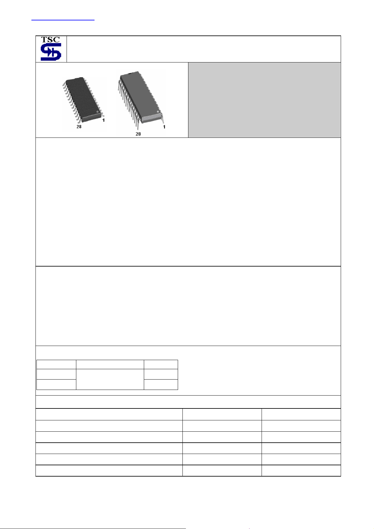
SOP-28 DIP-28
Voice Switched Speakerphone Circuit
Supply Voltage Range -1.0 V to 7.0V
IVB Current 500µA
Microphone Amplifier, & Hybrid Amplifier
Gain 40 dB
General Description
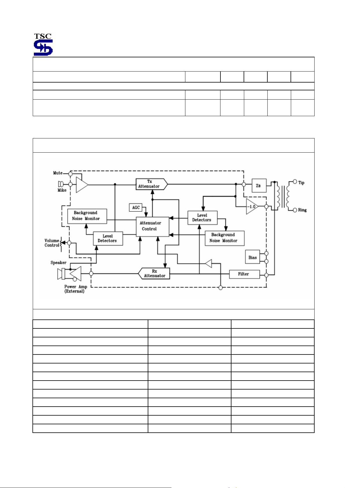
The TS34118 Voice Switched Speakerphone Circuit incorporates the necessary amplifiers, attenuators, level detectors,
and control algorithm to form the heart of a high quality hands-free speakerphone system. Included are a microphone
amplifier with adjustable gain and MUTE control, Transmit and Receive attenuators which operate in a complementary
manner, level detectors at both input and output of both attenuators, and background noise monitors for both the transmit
and receive channels. A Dial Tone Detector prevents the dial being attenuated by the Receive background noise monitor
circuit. Also included are two line drive amplifiers which can be used to form a hybrid network in conjunction with an
external coupling transformer. A high-pass filter can be used to filter out 60Hz noise in the receive channel, or for other
filtering functions .A Chip Disable pin permits powering down the entire circuit to conserve power on long loops where
loop current is at a minimum.
The TS34118 may be operated from a power supply, or it can be powered from the telephone line, requiring typically
5.0mA. The TS34118 can be interfaced directly to Tip and Ring (through a coupling transformer) for stand-alone
operation, or it can be used in conjunction with a handset speech network and/or other features of a feature phone
Features
Improved attenuator gain range: 52dB between
transmit and receive.
Low voltage operation for line-powered applications
(3.0-6.5V).
4-point signal sensing for improved sensitivity.
Back ground noise monitors for both transmit
and receive paths.
Standard 28-pin plastic DIP package and SOP
package available.
Microphone amplifier gain set by external
resistors-mute function included.
Chip disable for active/standby operation.
On board filter pinned-out for user defined function.
Dial tone detector to inhibit receive idle mode during
dial tone presence.
Compatible with TS34119 speaker amplifier.
Ordering Information
Part No. Operating Temp. Package
TS34118CD DIP-28
-20 ~ +70
TS34118CS
o
C
SOP-28
Absolute Maximum Rating
Description Value Unit
Supply voltage (pin 4) -1.0, +7.0
Voltage at CD (pin 3), MUT (pin 12) -1.0,Vcc +1.0
Voltage at VLC (pin 13) -1.0,Vcc +0.5
Voltage at TXI (pin 9),RXI (pin 21),FI(pin 2) -0.5,Vcc +0.5
Storage temperature range -65 to +150
TS34118 1-20 2004/09 rev. B
V
V
V
V
o
C
Recommended Operating Conditions
Description
Min. Typ. Max. Units
Supply voltage (pin 4) (see Text) 3.5 -- 6.5 V
CD input (pin 3), MUT input (pin 12) 0 -- Vcc V
IVB current (pin 15) - -- 500 µA
VLC (pin 13) 0.3xVB -- VB V
Attenuator input signal voltage (pin 9,21) 0 -- 350 mVrms
Microphone amplifier, Hybrid amplifier gain 0 -- 40 dB
Load current @RXO, TXO (pins 8,22)
@MCO (pin 10)
@HTO-, HTO+ (pin 6,5)
0
0
0
--
--
--
±2.0
±1.0
±5.0
mA
Ambient operating temperature range -20 -- +60 ℃
Electrical Characteristics (T
=+25, Vcc=5.0V, CD≤ 0.8V, unless noted)
A
Parameter Symbol Min Typ Max Unit
Power Supply
Vcc supply current (Vcc=6.5V, CD=0.8V)
(Vcc=6.5V, CD=2.0V)
CD input resistance (Vcc=VCD=6.5V)
CD input voltage - High
- Low
VB output voltage (Vcc=3.5V)
(Vcc=5.0V)
VB output resistance (IVB=1.0mA) R
VB power supply rejection ratio (CVB=220µF,f=1.0KHz)
PSRR -- 54 -- dB
Icc
R
CD
V
CDH
V
CDL
V
B
-- 400 -- Ω
OVB
--
--
50
2.0
0
--
1.8
5.5
600
90
--
--
1.3
2.1
8.0
800
--
Vcc
0.8
--
2.4
mA
µA
KΩ
V
V
V
Attenuators (T
=+25℃)
A
Receive attenuator gain (f=1.0KHz, VLC=VB )
Rx model, RXI=150mVrms (Vcc=5.0V)
Rx model, RXI=150mVrms (Vcc=3.5V)
Gain change –Vcc=3.5V versus Vcc=5.0V
AGC gain change –Vcc=2.8V versus Vcc=5.0V*
Idle model, RXI=150mVrms
Range (Rx to Tx model)
∆G
∆G
G
∆G
Volume control range (Rx model, 0.3VB<VLC<VB)
RXO DC voltage (Rx model)
∆RXO DC voltage (Rx to Tx model)
RXO high voltage (Iout=-1.0mA RXI=VB+1.5V)
RXO low voltage (Iout=+1.0mA, RXI=VB-1.0,
Output measured with respect to V
)*
B
RXI input resistance (RXI<350mVrms)
V
∆V
V
V
R
Transmit attenuator gain (f=1.0KHz)
Tx model , TXI=150mVrms
Idle model, TXI=150mVrms
Range (Tx to Rx model)
∆G
TXO DC voltage (Tx model) V
∆TXO DC voltage (Tx to Rx model) ∆V
TXO High voltage (Iout=-1.0mA TXI=VB+1.5V) V
TXO Low voltage (Iout=+1.0mA TXI=VB-1.0V,
Output measured with respect to VB)*
V
G
RX
G
RX
RX1
RX2
RX1
RX3
27 35 -- dB
V
CR
-- VB -- V
RXO
-- ±10 ±150 mV
RXO
3.7 -- -- V
RXOH
-- -1.5 -1.0 V
RXOL
7.0 10 14 KΩ
RXI
G
TX
G
TXI
TXI
-- VB -- V
TXO
-- ±30 ±150 mV
TXO
3.7 -- -- V
TXOH
-- -1.5 -1.0 V
TXOL
+4.0
+4.0
-0.5
--
-22
49
+4.0
-22
49
+6.0
+6.0
0
-25
-20
52
+6.0
-20
52
+8.0
+8.0
+0.5
-15
-17
54
+8.0
-17
54
dB
dB
TS34118 2-20 2004/09 rev. B
Electrical Characteristics (T
Parameter Symbol Min Typ Max Unit
Attenuators-continued (TA=+25℃)
TXI input resistance (TXI<350mVrms) R
Gain tracking (G
Attenuator Control (T
CT voltage (pin 14-VB) Rx model (VLC=VB)
CT source current(switching to Rx mode) I
CT sink current(switching to Tx mode) I
CT slow idle current I
CT fast idle internal resistance RFI 1.5 2.0 3.6 KΩ
Microphone Amplifier (T
Output offset (V
Open loop gain (f<100Hz) A
Gain bandwidth GBWM -- 1.0 -- MHz
Output High voltage (Iout=-1.0mA, Vcc=5.0V) V
Output Low voltage (Iout=+1.0mA) V
Input bias current (@MCI) IBM -- -40 -- nA
Muting (∆Gain) (f=1.0KHz, V
(300Hz<f<10KHz)
MUT input resistance (Vcc=V
MUT Input-High V
MUT Input-Low V
Hybrid Amplifiers (TA=+25 )℃
HTO-offset(V
HTO- to HTO+ offset (Feedback R=51KΩ) HB
Open loop gain(HTI to HTO-, f<100Hz) A
Gain bandwidth GBWH -- 1.0 -- MHz
Closed loop gain(HTO- to HTO+) A
Input bias current(@HTI) IBH -- -30 -- nA
HTO- High voltage (Iout=-5.0mA) V
HTO- Low voltage (Iout=+5.0mA) V
HTO+ High voltage (Iout=-5.0mA) V
HTO+ Low voltage (Iout=+5.0mA) V
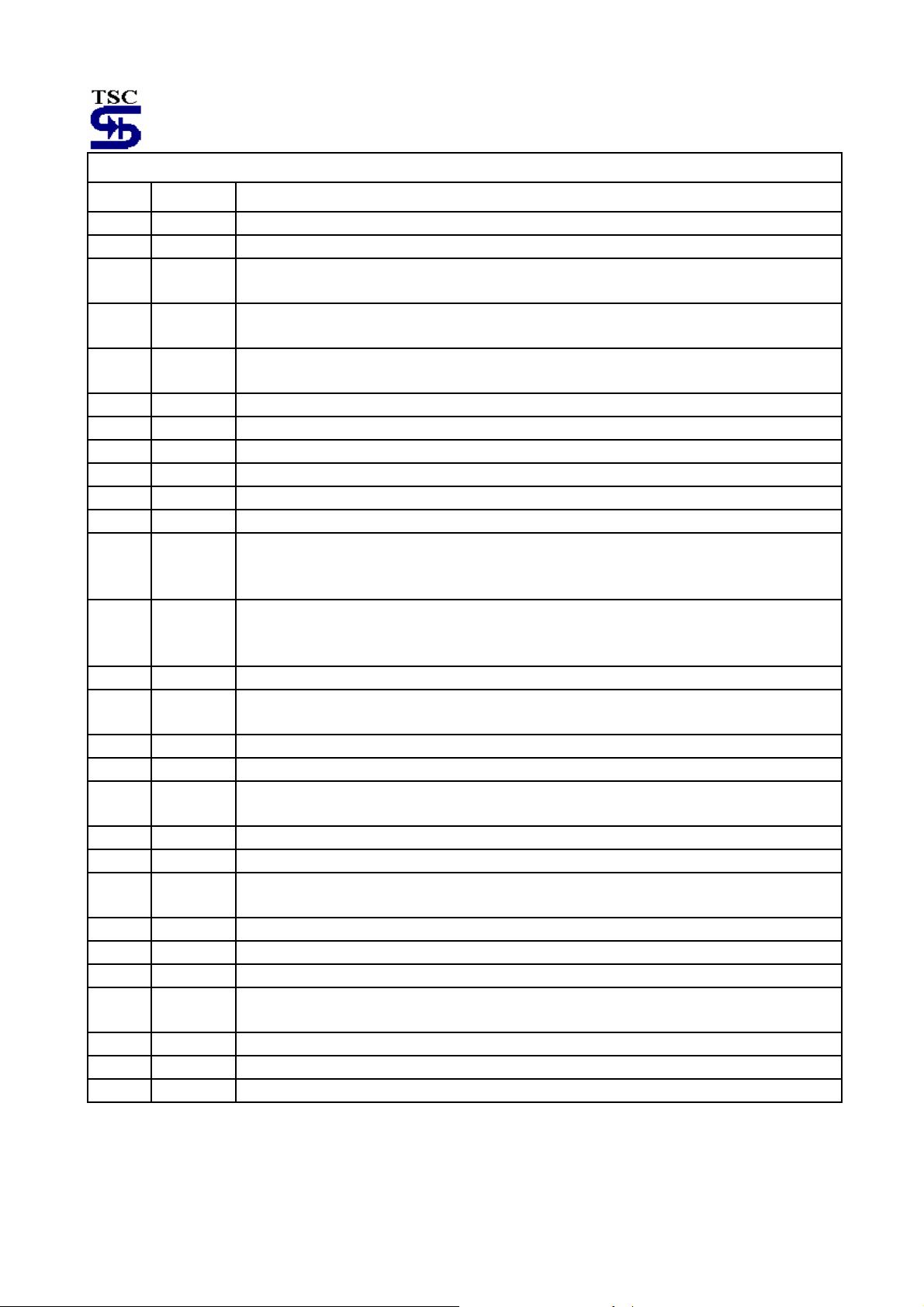
Distortion(300Hz<f<10KHz, see Figure 1) THDH -- 0.3 -- %
Level Detectors and Background Noise Monitors (T
Transmit-Receive switch threshold
(Ratio of current at RLI1 + RLI2 to 20µA
at TLI1 + TLI2 to switch from Tx to Rx)
Source current at RLO1, RLO2, TLO1, TLO2 I
Sink current at RLO1, RLO2, TLO1, TLO2 I
CPR, CPT output resistance (Iout=1.5mA) RCP -- 35 -- Ω
CPR, CPT leakage current I
Filter (TA=+25℃)
Voltage offset at FO (VFO-VB, 220KΩ from VB to FI) FO
FO sink current IFO 150 260 400 µA
FI bias current IFI -- -50 -- nA
+ GTX, @ Tx, Idle, Rx)* GTR -- ±0.1 -- dB
RX
=+25℃)
A
Idle model
Tx model
=+25℃,V
A
, feedback R=180KΩ) MCOvos -50 0 +50 mV
MCO-VB
=2.0V)
MUT
MUT
, Feedback R=51KΩ) H
HTO- -VB
=+25, Vcc=5.0V, CD≤ 0.8V, unless noted)
A
MUT
≤0.8V,A
=31dB unless otherwise noted)
VCL
=6.5V) R
=+25℃)
A
7.0 10 14 KΩ
TXI
--
V
CT
--
--
-85 -60 -40 µA
CTR
+40 +60 +85 µA
CTT
-- 0 -- µA
CTS
70 80 -- dB
VOLM
3.7 -- -- V
MCOH
-- -- 200 mV
MCOL
GMT
50 90 -- KΩ
MUT
2.0 -- Vcc V
MUTH
0 -- 0.8 V
MUTL
-20 0 +20 mV
VOS
-30 0 +30 mV
VOS
60 80 -- dB
VOLH
-0.35 0 +0.35 dB
VCLH
3.7 -- -- V
HT-H
-- -- 250 mV
HT-L
3.7 -- -- V
HT+H
-- -- 450 mV
HT+L
0.8 1.0 1.2
I
TH
-- -2.0 -- mA
LSO
-- 4.0 -- µA
LSK
-- -0.2 -- µA
CPLK
-200 -90 0 mV
VOS
-55
--
+240
0
-240
--
-68
--
--
--
--
--
mV
dB
TS34118 3-20 2004/09 rev. B
Electrical Characteristics (T
Parameter Symbol Min Typ Max Unit
System Distortion (TA=+25℃, f=1.0KHz)
Rx mode (from FI to RXO, FO connected to RXI)
Tx mode (from MCI to HTO-/HTO+, includes
Tx attenuator)
1. All currents into a device pin are positive, those out of a pin are negative. Algebraic convention rather than magnitude
is used to define limits.
=+25, Vcc=5.0V, CD≤ 0.8V, unless noted)
A
THDR -- 0.5 3.0 %
THD
-- 0.8 3.0 %
T
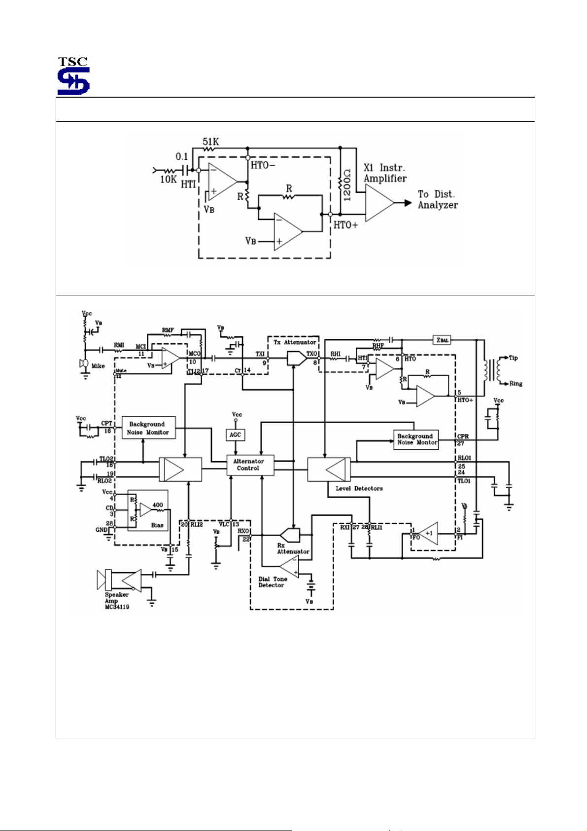
Simplified Block Diagram
Temperature Characteristics
Parameter Typical Value @25℃ Typical Change –20 to +60℃
Vcc supply current (CD=0.8V) 5.0mA -0.3%/℃
Vcc supply current (CD=2.0V) 400µA -0.4%/℃
VB output voltage (Vcc=5.0V) 2.1V +0.8%/℃
Attenuator gain (Max Gain) +6.0dB 0.0008dB/℃
Attenuator gain (Max attenuation) -46dB 0.004dB/℃
Attenuator input resistance (@ TXI, RXI) 10KΩ +0.6%/℃
Dial tone detector threshold 15mV +20µV/℃
CT source, sink current ±60µA -0.15%/℃
Microphone, Hybrid amplifier offset 0 mV ±4.0µV/℃
Transmit-Receive switching threshold 1.0 ±0.02%/℃
Sink current at RLO1, RLO2, TLO1, TLO2 4.0µA -10nA/℃
Closed loop gain (HTO- to HTO+) 0 dB 0.001%/℃
TS34118 4-20 2004/09 rev. B
Pin Function Description
Pin Name Description
1 FO Filter output. Output impedance is less than 50 ohms.
2 FI Filter input. Input impedance is greater than 1.0Mohm.
3 CD
4 Vcc
5 HTO+
6 HTO- Output of the first hybrid amplifier. The gain of the amp is set by external resistors.
7 HTI Input and summing node for the first hybrid amplifier . DC level is≈VB.
8 TXO Output of the transmit attenuator. DC level is approximately VB.
9 TXI Input to the transmit attenuator. Max. Signal level is 350m Vrms . Input impedance is 10KΩ.
10 MCO Output of the microphone amplifier. The gain of the amplifier is set by external resistors.
11 MCI Input and summing node of the microphone amplifier. DC level is≈ VB.
12 MUT
13 VLC
14 CT An RC at this pin sets the response time for the circuit to switch modes.
15 VB
16 CPT An RC at this pin sets the time constant for the transmit background monitor.
17 TLI2 Input to the transmit level detector on the mike/speaker side.
18 TLO2
19 RLO2 Output of the receive level detector on the mike/speaker side.
20 RLI2 Input to the receive level detector on the mike/speaker side.
21 RXI
22 RXO Output of the receive attenuator. DC level is approximately VB.
23 TLI1 Input to the transmit level detector on the line side.
24 TLO1 Output of the transmit level detector on the line side.
25 RLO1
26 RLI1 Input to the receive level detector on the line side.
27 CPR An RC at this pin sets the time constant for the receive background monitor.
28 GND Ground pin for the entire IC.
Chip Disable. A logic low(<0.8V) sets normal operation. A logic high (>2.0V) disables the IC to
conserve power. Input impedance is norminally 90KΩ.
A supply voltage of +2.8 to +6.5 volts is required, at ≈5.0mA. As Vcc falls from 3.5 to 2.8volts,
an AGC circuit reduces the receive attenuator gain by ≈25dB (when in the receive mode).
Output of the second hybrid amplifier. The gain is internally set at –1.0 to provide a differential
output, in conjunction with HTO-, to the hybrid transformer.
Mute input. A logic low(<0.8V) sets normal operation. A logic high (>2.0V) mutes the
microphone amplifier without affecting the rest of the circuit. Input impedance is norminally
90KΩ.
Volume control input. When VLC=V
receive mode. When VLC=0.3V
mode.
An output voltage≈Vcc/2. This voltage is a system ac ground, and biases the volume control. A
filter cap is required
Output of the transmit level detector on the mike/speaker side, and input to the transmit
background monitor.
Input to the receive attenuator and dial tone detector. Max input level is 350mV RMS. Input
impedance is ≈10KΩ.
Output of the receive level detector on the line side, and input to the receive background
monitor.
, the receive attenuator is at maximum gain when in the
B
, the receive gain is down 35dB. Does not affect the transmit
B
TS34118 5-20 2004/09 rev. B
Typical Application Circuit
Figure 1. Hybrid Amplifier Distortion Test
Figure 2. TS34118 Block Diagram
TS34118 6-20 2004/09 rev. B
Introduction
The fundamental difference between the operation of a speakerphone and a handset is that of half-duplex versus full
duplex. The handset is full duplex since con-version can occur in both directions (transmit and receive) simultaneously.
A speakerphone has higher gain levels in both paths and attempting to converse full duplex results in oscillatory
problems due to the loop that exists within the system. The loop is formed by the receive and transmit paths, the hybrid,
and the acoustic coupling (speaker to microphone). The only practical and economical solution used to data is to design
the speakerphone to function in a half duplex mode – i.e. only one person speaks at a time, while the other listens. To
achieve this required a circuit which can detect who is talking, switch on the appropriate path (transmit or receive) and
switch off (attenuate) the other path. In this way, the loop gain is maintained less than unity. When the talkers exchange
function, the circuit must quickly detect this, and switch the circuit appropriately. By providing speech level detectors the
circuit operates in a “hands free” mode, eliminating the need for a “push to talk” switch.
The handset by the way, has the same loop as the speakerphone. But since the gains are considerably lower, and
since the acoustic compiling from the earpiece to the mouthpiece is almost non existent (the receiver is normally held
against a person’s eat.) oscillations don’t occur.
The TS341118 provides the necessary level detectors, attenuators, and switching control for a properly operating
speakerphone. The detection sensitivity and timing are externally controllable. Additionally, the TS34118 provides
background nodule monitor’s which make the circuit insensitive to room and line noise, hybrid amplifier, and other
associated functions, please refer to the Block Diagram (Figure 2) when reading the following sections.
Attenuators
The transmit and receive attenuators are complementary in function. i .e. when one is at maximum gain (+6.0dB), the
other is at maximum attenuation (-4.5dB), and vice verse. They sum of their gains remains constant (within a nominal
error hand of ±0.1dB) at a typical value of ~40dB (see Figure 10). Their purpose is to control the transmit and receive
paths to provide the half-duplex operation required in a speakerphone.
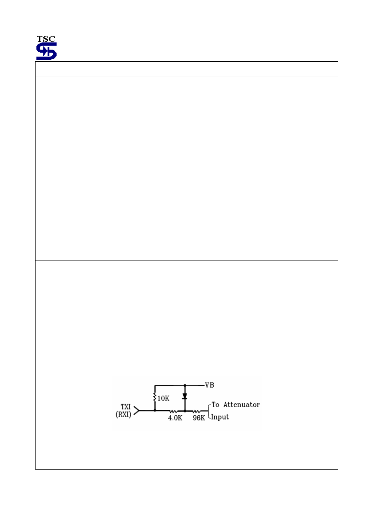
The attenuators are non-inverting, and have a –3.0dB (from max gain) frequency of 100KHz. The input impedance of
each attenuator (TXI and RXI) is nominally 10KΩ (see Figure 3), and the input signal should be limited to 350mVrms
(990mVp-p) to prevent distortion. That maximum recommended input signal is independent of the volume control
setting. The diode clamp on the inputs the input swing, and therefore the maximum negative output swing. This is the
reason for V
impedance is 10Ω until the output current limit typically 2.5mA) is reached.
RXOL
and VT
specification being defined as they are in the Electrical Characteristics. The output
XOL
Figure 3. Attenuator Input Stage
TS34118 7-20 2004/09 rev. B

Attenuators
The attenuators are controlled by the single output of the Control Block, which is measurable at the CT pin (pin 14).
When the C
+6.0dB). When the C
attenuator is at +6.0dB). The circuit is in an idle mode when the C
to be halfway between their fully on and fully off positions (-20dB each). Monitoring the C
the most direct method of monitoring the circuit’s mode.
The inputs to the Control Block are seven, 2 from the comparators operated by the level detectors, 2 from the
background noise monitors, the volume control, the dial-tone detector, and the AGC circuit. These seven inputs are
described below.
pin is at +240 millivolts with respect to VB, the circuit is in the receive mode (receive attenuator is at
T
voltage is at +240 millivolts with respect to VB, the circuit is in the transmit mode (transmit
T
voltage is equal to VB. Causing the attenuators gain
T
voltage (with respect to VB) is
T
Level Detectors
There are four level detectors-two on the receive side and two on the transmit side. Refer to Figure 4. The terms in
parentheses from one system, and the other terms from one system. Each level detector is a high gain amplifier with
back-to-bank diodes in the feedback path, resulting in non-linear gain, which permits operation over a wide dynamic
range of speech levels. The sensitivity of each level detector is determined by the external resistor and capacitor at
each input (TLI1, TLI2, RLI1 and RLI2). Each output charge an external capacitor through a diode and limiting resistor,
thus providing a do representation of the input as signal level. The outputs have a quick rise time (determined by the
capacitor and an internal 350Ω resistor), and a slow decay time set by an internal current source and the capacitor. The
capacitors on the four outputs should have the same value (±10%) to prevent timing problems. Referring to Figure 2, on
the receives side, one level detector (RLI1) is at the receive input receiving thus same signal as at Tip and Ring, and
the other (PLI2) is at the output of the speaker amplifier. On the transmit side, one level detector (TLI2) is at the output
of the microphone amplifier, while the other (TLI1) is at the hybrid output. Outputs RLO1 and TLO1 feed a comparator,
the output of which goes to the Attenuator Control Block. Likewise, outputs RLO2 and TLO2 feed a second comparator
which also goes to the Attenuator Control Block. The touch table for the effects of the level detectors on the Control
Block is given in the section describing the Control Block.
Figure 4. Level Detectors
TS34118 8-20 2004/09 rev. B

Background Noise Monitors
The purpose of the background noise monitors is to distinguish speech (which consists of bursts) from background noise
(a relatively constant signal level). There are two background noise monitors-one for the receive path and one for the
transmit path. Referring to Figure 4, the receive background noise monitor is operated on by the RLI1-PLO1 level
detector, while the transmit background noise monitor is operated on by the TLI2-TLO2 level detector. They monitor the
background noise by storing a dc voltage representative of the respective noise levels in capacitors at CPR and CPT.
The voltages at these pins have slow rise times (determined by the external RC), but fast decay times. If the signal at
RLI1 (or TLI2) changes slowly, the voltage at CPR (or CPT) will remain more positive than the voltage at the non-inverting
input of the monitor’s output comparator. When speech is present, the voltage on the non-inverting input of the
comparator will rise quicker than the voltage at the inverting input (due to the burst characteristic of speech), causing its
output to change. This output is sensed by the Attenuator Control Block.
The 36mV offset at the comparator’s input keeps the comparator from changing state unless the speech level exceeds
the background noise by≈4.0dB. The time constant of the external RC (≈4.7 seconds) determines the response time to
background noise variations.
Volume Control
The volume control input at VLC (pin 13) is sensed as a voltage with respect to V
attenuators only in the receive mode. It has no effect in the idle or transmit modes.
When in the receive mode, the gain of the receive attenuator will be +6.0dB, and the gain of the transmit attenuator will
be –46dB only when VLC is equal to V
Figure 14), and the gain of the transmit attenuator is increased such that their sum remains constant. Changing the
voltage at VLC changes the voltage at C
attenuators.
The volume control setting does not affect the maximum attenuator input signal at which noticeable distortion occurs. The
bias current at VLC is typically 60nA out of the pin, and does not vary significantly with the VLC voltage or with Vcc.
. As VLC is reduced below VB, the gain of the receive attenuator is reduced (see
B
(see the Attenuator Control Block section), which in turn controls the
T
The volume control affects the
B.
Dial Tone Detectors
The dial tone detector is a comparator with one side connected to the receive input (RXI) and the other input connected
with a 15mV offset (see Figure 5). If the circuit is in the receive mode, and the incoming signal is greater than 15mV
to V
B
(10mVrms), the comparator’s output will change, disabling the receive idle mode. The receive attenuator will then be at a
setting determined solely by the volume control.
The purpose of this circuit is to prevent the dial tone (which would be considered as continuous noise) from fading away
as the circuit would have the tendency to switch to the idle mode. By disabling the receive idle mode, the dial tone
remains at the normally expected full level.
Figure 5. Dial Tone Detectors
TS34118 9-20 2004/09 rev. B

Attenuator Control Block
The Attenuator Control Block has the seven inputs described above:
-The output of the comparator operated by RLO2 and TLO2 (microphone/speaker side) - designated C1.
-The output of the comparator operated by RLO1 and TLO1 (TIP/Ring side) – designated C2.
-The output of the transmit background noise monitor – designated C3.
-The output of the receive background noise monitor
-designated C4.
-The volume control.
-The dial tone detector.
-The AGC circuit.
The single output of the Control Block controls the two attenuators. The effect of C1-C4 is as follows:
Input Output
C1 C2 C3 C4 Mode
Tx Tx 1 X Transmit
Tx Rx Y Y Fast Idle
Rx Tx Y y Fast Idle
Rx Rx X 1 Receive
Tx Tx 0 X Slow Idle
Tx Rx 0 0 Slow Idle
Rx Tx 0 0 Slow Idle
Rx Rx X 0 Slow Idle
X=Don’t Care; y=C3 and C4 are not both 0. A definition of the above terms:
1)”Transmit” means the transmit attenuator is fully on (+6.0dB), and the receive attenuator is at max. attenuation
(-46dB).
2)”Receive” means both attenuators are controlled by the volume control. At max. Volume, the receive attenuator is fully
on (+6.0dB), and the transmit attenuator is at max. attenuation (-46dB).
3)”Fast Idle” means both transmit and receive speech is present in approximately equal levels. The attenuators are
quickly switched (30ms) to idle until one speech level dominates the other.
4)”Slow Idle” means speech has ceased in both transmit and receive paths. The attenuators are then slowly switched (1
second) to the idle mode.
5) Switch to the full transmit or receive modes from any other mode is at the fast rate (≈30ms).
A summary of the truth table is as follows:
1)The circuit will switch to transmit if: a) both transmit level detectors sense higher signal levels relative to the respective
receive level detectors (TLI1 versus RLI1, TLI2 versus RLI2), and b) the transmit background noise monitor indicates
the presence of speech.
2)The circuit will switch to receive if: a) both receive level detectors sense higher signal levels relative to the respective
transmit level detectors, and b) the receive background noise monitor indicates the presence of speech.
3) The circuit will switch to the fast idle mode if the level detectors disagree on the relative strengths of the signal
levels, and at least one of the background noise monitors indicates speech. For example, referring to the Block
Diagram (Figure 2), if there is sufficient signal at the microphone amp output (TLI2) to override the speaker signal
(RLI2), and there is sufficient signal at the receive input (RLI1) to override the signal at the hybrid output (TLI1), and
either or both background monitors indicate speech, then the circuit will be in the fast idle mode. Two conditions
which can cause the fast idle mode to occur are a) when both talkers are attempting to gain control of the system by
talking at the same time, and b)when one talker is in a very noisy environment, forcing the other talker to continually
override that noise level. In general, the fast idle mode will occur infrequently.
TS34118 10-20 2004/09 rev. B

Attenuator Control Block
4) The circuit will switch to the slow idle mode when a) both talkers are quiet (no speech present), or b) when one talker’s
speech level is continuously overridden by noise at the other speaker’s location.
The time required to switch the circuit between transmit, receive, fast idle and slow idle is determined in part by the
components at the CT pin (pin 14). (see the section on Switch Time for a more complete explanation of the switching
time components). A schematic of the CT circuitry is shown in Figure 6, and operates as follows:
-RT is typically 120KΩ, and CT is typically 5.0µF.
-To switch to the receive mode, I1 is turned on (I2 is off), charging the external capacitor to +240mV above VB. (An
internal clamp prevents further charging of the capacitor.)
-To switch to the transmit mode, I2 is turned on (I1 is off) bringing down the voltage on the capacitor to –240mV with
respect to VB.
-To switch to idle quickly (fast idle), the current sources are turned off, and the internal 2.0KΩ resistor is switched in,
discharging the capacitor to VB with a time constant = 2.0K×CT.
-To switch to idle slowly (slowly idle), the current sources are turned off, the switch at the internal 2.0KΩ resistor is
open, and the capacitor discharges to VB through the external resistor RT with a time constant = RT × CT.
Figure 6. CT Attenuator Control Block Circuit
Microphone Amplifier
The microphone amplifier (pins 10,11) has the non-inverting input internally connected to VB, while the inverting input and
the output are pinned out. Unlike most op-amps, the amplifier has an all-NPN output stage, which maximizes phase
margin and gain-bandwidth. This feature ensures stability at gains less than unity, as well as with a wide range of reactive
loads. The open loop gain is typically 80dB (f<100Hz), and the gain-bandwidth is typically 1.0MHz (see Figure 16). The
maximum p-p output swing is typically 1.0 volt less than Vcc with an output impedance of <10 Ω until current limited is
reached (typically 1.5mA).Input bias current at MCI is typically 40nA out of the pin.
The muting function (Pin 12), when activated, will reduce the gain of the amplifier to ≈-39dB (with RMI=5.0KΩ) by shorting
output to the inverting input (see Figure 7). The mute input has a threshold of ≈1.5 volts, and the voltage at this pin must
be kept within the range of ground and Vcc (see Figure 17). If the mute function is not used, the pin should be grounded.
TS34118 11-20 2004/09 rev. B

Microphone Amplifier
Figure 7. Microphone Amplifier and Mute
Hybrid Amplifiers
The two hybrid amplifiers (at HTO+, HTO-, and HTI), in conjunction with an external transformer, provide the two-to four
wire converter for interfacing to the telephone line. The gain of the first amplifier (HTI to HTO-) is set by external resistors
(gain=-R
most op-amps, the amplifiers have all-NPN output stage, which maximizes phase margin and gain-bandwidth. This
feature ensures stability at gains less than unity, as well as with a wide range of reactive loads. The open loop gain of the
first amplifier is typically 80dB , and the gain bandwidth of each amplifier is ≈1.0MHz (see Figure 16). The maximum p-p
output swing of each amplifier is typically 1.2 volts less than Vcc with an output impedance of <10Ωuntil current limiting is
reached (typically 8.0mA). The output current capability is guaranteed to be a minimum of 5.0mA. The bias current at HTI
is typically 30nA out of the pin.
The connections to the coupling transformer are shown in the Block Diagram (Figure 2). The block labeled Zbal is the
balancing network necessary to match the line impedance.
in Figure 2), and its output drives the second amplifier, the gain of which is internally set at –1.0. Unlike
HF/PHI
Filter
The operation of the filter circuit is determined by the external components. The circuit within the TS34118, from pins FI to
FO is a buffer with a high input impedance (>1.0MΩ), and a low output impedance (<50Ω). The configuration of the
external components determines whether the circuit is a high-pass filter (as shown in Figure 2), a low-pass filter, or a
band-pass filter.
As a high pass filter, with the components shown in Figure 8, the filter will keep out 60Hz (and 120Hz) hum which can be
picked up by the external telephone lines.
Figure 8. High Pass Filter
TS34118 12-20 2004/09 rev. B

Filter
As a low pass filter (Figure 9), it can be used to roll off the high end frequencies in the receive circuit, which aids in
protecting against acoustic feedback problems. With an appropriate choice of an input coupling capacitor to the low
pass filter is formed
Figure 9. Low Pass Filter
Power Supply, VB, and Chip Disable
The power supply voltage at Vcc (pin 4) is to be between 3.5 and 6.5 volts for normal operation, with reduced operation
possible down to 2.8 volts. The power supply current is shown in Figure 18 for both the power-up and power-down
mode.
The output voltage at V
is ≈400Ω and in conjunction with the external capacitor at VB, forms a low pass filter for power supply rejection with
V
B
different capacitors. The choice of capacitor is application dependent base on whether the circuit is powered by the
telephone line or a power supply.
Since V
biases the microphone and hybrid amplifiers, the amount of supply rejection at their outputs is directly related
B
to the rejection at V
The Chip Disable (pin 3) permits powering down the IC to conserve power and/or for muting purposes. With CD≤0.8
volts, normal operation is in effect. With CD ≥ 2.0 volts and ≤Vcc, the IC is powered down. In the powered down mode,
the microphone and the hybrid amplifiers are disable, and their outputs go to a high impedance state. Additionally, the
bias is removed from the level detectors. The bias is not removed from the filter (pins 1,2). The attenuators (pin 8,9, 21,
22), or from pin 13,14, and 15 (the attenuators are disabled, however, and will not pass a signal). The input impedance
at CD is typically 90KΩ, has a threshold of ≈ 1.5 volts, and the voltage at this pin must be kept within the range of
ground and Vcc . If CD is not used, the pin should be grounded.
(pin 15) is ≈ (Vcc-0.7)/2, and provides the ac ground for the system. The output impedance at
B
, as well as their respective gains. Depicts this graphically.
B
Switching Time
The switching time of the TS34118 circuit is dominated by the components at CT (pin 14, refer to Figure 6), and
secondarily by the capacitors at the level detector outputs (RLO1, RLO2, TLO1, TLO2).
The time to switch to receive or to transmit from idle is determined by the capacitor at C
current sources (refer to Figure 6). The switching time is:
∆T=∆V × C
T
/ I
For the typical cause where ∆V=240mV, I=60µA. And CT is 50µF, ∆T=20ms. If the circuit switches directly from receive
to transmit (or vice-versa), the total switching time would be 40ms.
The switching time from either receive or transmit to idle depends on which type of idle mode is in effect. If the circuit is
going to “fast idle”, the time constant is determined by the C
C
= 5.0µF, the time constant is ≈30ms (for 95% change). Fast idle is an infrequent occurrence, however, occurring
T
capacitor, and the internal 2.0KΩ resistor (Figure 6). With
T
when both speakers are talking and competing for control of the circuit. The switching time from idle back to either
transmit or receive is described above.
TS34118 13-20 2004/09 rev. B
, together with the internal
T

Switching Time
If the circuit is switching to “slow idle”, the time constant is determined by the CT capacitor and RT, the external resistor
(see Figure 6). With C
= 5.0µF, and RT = 120KΩ, the time constant is ≈600ms, giving a switching time of ≈ 1.8 seconds
T
(for 95% change). The switching period to slow idle begins when both speakers have stopped talking. The switching
time back to the original mode will depend on how soon that speaker begins speaking again. The sooner the speaking
time starts during the 1.8 seconds period, the quicker the switching time since a smaller voltage excursion is required.
That switching time is determined by the internal current sources as described above.
The above switching times occur, however, after the level detectors have detected the appropriate signal levels, since
their outputs operate the Attenuator Control Block. Referring to Figure 4, the rise time of the level detector’s outputs to
new speech is quick by comparison (≈1.0ms), determined by the internal 350Ωresistor and the external capacitor
(typically 2.0µF). The output’s decay time is determined by the external capacitor, and an internal 4.0µF current source
giving a decay rate of ≈60ms for 120mV excursion at RLO or TLO. However, the overall response time of the circuit is
not a constant since it depends on the relative strength of the signals at the different level detectors, as well as the
timing of the signals with respect to each other. The capacitors at the four outputs (RLO1, RLO2, TLO1, TLO2) must be
equal value (±10%) to prevent problems in timing and level response.
The rise time of the level detector’s outputs is not significant since it is so short. The decay time, however, provides a
significant part of the “hold time” necessary to hold the circuit during the normal pauses in speech.
The components at the inputs of the level detectors (RLI1, RLI2, TLI1,TLI2) do not affect the switching time, but rather
affect the relative signal levels required to switch the circuit, as well as the frequency response of the detectors.
Design Equations
Referring to Figure 10(the coupling capacitors have been omitted for simplicity), the following definitions will be used (all
measurements are at 1.0KHz)
-G
is the gain of the microphone amplifier measured from the microphone output to TXI (typically 35V/V, or 31dB);
MA
-G
is the gain of the transmit attenuator, measured from TXI to TXO;
TX
-G
is the gain of hybrid amplifiers, measured from TXO to the HTO-/HTO+ differential output (typically 10.2V/V, or
HA
20.1dB);
-G
is the gain from HTO-/HTO+ to Tip/Ring for transmit signals, and includes the balance network (measured at
HT
0.4V/V, or –8.0dB);
-G
is the side tone gain, measured from HTO-/HTO+ to the filter input (measured at 0.18V/V , or –15dB);
ST
-G
is the gain from Tip/Ring to the filter input for receive signals (measured at 0.833V/V or –1.6dB);
HR
-G
is the gain of the filter stage, measured from the input of the filter to RXI, typically 0dB at 1.0KHz;
FO
-G
is the gain of the receive attenuator measured from RXI to RXO;
RX
-G
is the gain of the speaker amplifier, measured from RXO to the differential output of the TS34119 (typical 22V/V
SA
or 26.8dB);
-G
is the acoustic coupling, measured from the speaker differential voltage to the microphone output voltage.
AC
I) Transmit Gain
The transmit gain, from the microphone output (VM) to tip and Ring, is determined by the output characteristics of the
microphone, and the desired transmit level. For example, a typical electret microphone will produce ≈0.35mVrms under
normal speech conditions. To achieve 100mVrms at Tip / Ring, an overall gain of 285V/V is necessary. The gain of the
transmit attenuator is fixed at 2.0 (+6.0dB), and the gain through the hybrid normally 0.4 (-8.0dB). Therefore a gain of
357V/V is required of the microphone and hybrid amplifiers. It is desirable to have the majority f that gain in the
microphone amplifier for three reasons:
1) The low level signals from the microphone should be amplifier as soon as possible to minimize signal/noise
problems.
TS34118 14-20 2004/09 rev. B

×
Design Equations
2) To provide a reasonable signal level to the TLI2 level detector; and 3)to minimize any gain applied to broadband
noise generated within the attenuator. However, to cover the normal voice band, the microphone amplifier’s gain
should not exceed 48dB. For the circuit of Figure 10, the gain of the microphone amplifier was set at 35V/V (31dB),
and the differential gain of the hybrid amplifiers was set at 10.2V/V (20.1dB).
II) Receive Gain
The overall receive gain depends on the incoming signal level, and the desired output power at the speaker. Normal
receive levels (independent of the peaks) at Tip/Ring can be 35mVrms (-27dBm). Although on long lines That level can
be down to 8.0mVrms (-40dBm).The speaker power is:
PSPK =
0.610dBm/10
(Equation 1)
Rs
Where R
path. Experience has shown that≈30dB gain is a satisfactory amount for the majority of applications. Using the above
numbers and Equation 1, it would appear that the resulting power to the speaker is extremely low. However, Equation 1
does not consider the peaks in normal speech, which can be 10 to 15 times the rms value. Considering the peaks, the
overall average power approaches 20-30mV on long lines, and much more on short lines.
Referring to Figure 10, the gain from Tip/Ring to the filter input was measured at 0.833V/V (-1.6dB), the filter’s gain is
unity, and the receive attenuator’s gain is 2.0V/V (+6.0dB) at maximum volume. The speaker amplifier’s gain is set at
22V/V (26.8dB), which puts the overall gain at ≈31.2dB.
III) Loop Gain
The total loop gain must add up to less than zero dB to obtain a stable circuit. This can be expressed as:
Using the typical numbers mentioned above, and knowing that GTX+GRX=-40dB, the required acoustic coupling can be
determined:
An acoustic loss of at least 23 dB is necessary to prevent instability and oscillations, commonly referred to as “singing.”
However, the following equations show that greater acoustic loss is necessary to obtain proper level detection and
switching.
is the speaker impedance, and the dBm term is the incoming signal level increased by the gain of the receive
S
GMA+GTX+GHA+GST+GFO+GRX+GSA+GAC<0 (Equation 2)
G
<-[31+20.1+(-15)+0+(-40)+26.8]=-22.9dB (Equation 3)
AC
IV) Switching Threshold
To switch comparator C1, currents I1 and I3 need to be determined. Referring to Figure 11, with a receive signal VL
applied to Tip/Ring, a current I3 will flow through R3 into RLI2 according to the following equation:
V
⎡
R3
L
⎢
⎣
GV
×
MAM
(Equation 5)
GGG
I3 =
Where the terms in the brackets are the V/V gain terms. The speaker amplifier gain is divided by two since G
differential gain of the amplifier, and V3 is obtained from one the side of the output. The current I1, coming from the
microphone circuit, is defined by:
I1 =
G
⎤
SA
×××
RXFOHR
(Equation 4)
⎥
2
⎦
is the
SA
R1
Where V
equations yields:
TS34118 15-20 2004/09 rev. B
is the microphone voltage. Since the switching threshold occurs when I1=I3, combining the above two
M
[]
VM = VL ×
R1
R3
××
MA
GGGG
SARXFOHR
2G
(Equation 6)
×

Design Equations
Figure 10. Basic Block Diagram For Design Purpos
This is the general equation defining the microphone voltage necessary to switch comparator C1 when a received
signal V
numbers for Equation 6 yields:
is present. The highest VM occurs when the receive attenuator is at maximum gain (+6.0dB). Using the typical
L
V
= 0.52VL (Equation 7)
M
To switch comparator C2, currents I2 and I4 need to be determined. With sound applied to the
microphone, a voltage V
V
⎡
I2 =
Since G
Comparator C2 switches when I4=I2. I4 is defined by:
I4 =
M
⎢
R2
⎣
is the differential gain of the hybrid amplifiers, it is divided by two to obtain the voltage V2 applied to R2.
HA
V
L
[]
R4
Setting I4=I2, and combining the above equations results in:
V
= VM ×
L
This equation defines the line voltage at Tip/Ring necessary to switch comparator C2 in the presence of a microphone
voltage. The highest V
Equation 10 yields:
V
=840VM (or VM=0.0019 VL) (Equation 11)
L
At idle, where the gain of the two attenuators is –20dB (0.1V/V), Equations 6 and 10 yield the same result:
VM=0.024VL (Equation 12)
R4
R2
is creased by the microphone, resulting in a current I2 into TLI1:
M
G
⎤
HA
××
GG
TXMA
GG × (Equation 9)
FOHR
[]
× (Equation 10)
[]
occurs when the circuit is in the transmit mode (G
L
(Equation 8)
⎥
2
⎦
××
GGG
HATXMA
2GG
××
FOHR
= +6.0dB). Using the typical numbers for
TX
Equations 7, 11 and 12 define the thresholds for switching, and are represented in the following graph:
TS34118 16-20 2004/09 rev. B

Design Equations
Figure 11. Switching Threshold
The “M” terms are the slopes of the lines (0.52,0.024, and 0.0019) which are the coefficients of the three equations.
The M
switch to transmit in the presence of a given receive signal level. The M
threshold, The M
necessary to overcome noise on the other.
Some comments on the above graph:
line represents the receive to transmit threshold in that it defines the microphone signal level necessary to
RX
line represents the transmit to receive
TX
line represents the idle condition, and defines the threshold level on one side (transmit or receive)
I
-Acoustic coupling and side tone coupling were not included in Equations 7 and 12. Those couplings will affect the
actual performance of the final speakerphone due to their interaction with speech at the microphone, and the
receive signal coming in at Tip/Ring. The effects of those couplings are difficult to predict due to their associated
phase shifts and frequency response. In some cases the coupling signal will add, and other times subtract from the
incoming signal. The physical design of the speakerphone enclosure, as well as the specific phone line to which it
is connected , will affect the acoustic and side tone couplings, respectively.
-The M
following equation:
line helps define the maximum acoustic coupling allowed in a system, which can be found from the
RX
R4
R1
××
GR22
××
FO
(Equation 13)
GR32
MA
(Equation 14)
AC-MAX
of –37dB.
G
=
AC-MAX
Equation 13 is independent of the volume control setting. Conversely, the acoustic coupling of a designed system helps
determine the minimum slope of that line. Using the component values in Equation 13 yields a G
Experience has shown, however, that an acoustic coupling loss of >40dB is desirable.
-The M
the following equation:
Using the component values in Equation 14 yields a maximum side tone of 0dB. Experience has shown, however, that
a minimum of 6.0dB loss is preferable.
The above equations can be used to determine the resistor values for the level detector inputs. Equation 6 can be used
to determine the R1/R3 ratio, and Equation 10 can be used to determine the R4/R2 ratio. In Figure 10, R1-R4 each
represent the combined impedance of the resistor and coupling capacitor at each level detector input. The magnitude of
each RC’s impedance should be kept within the range of 2.0K-15KΩ in the voice band (due to the typical signal levels
present) to obtain the best performance from the level detectors. The specific R and C at each location will determine
the frequency response of that level detector.
line helps define the maximum side tone coupling (GST) allowed in the system, which can be found from
TX
G
=
ST
TS34118 17-20 2004/09 rev. B

Application Information
Dial Tone Detector
The threshold for the dial tone detector is internally set at 15mV (10mVrms) below VB (see Figure 5). That threshold can
be reduced by connecting a resistor from RXI to ground. The resistor value is calculated from:
R =
Where V
RXI, the threshold can be increased. The resistor value is calculated from:
Where ∆V is the amount of threshold increase.
Background Noise Monitors
For testing or circuit analysis purposes, the transmit or receive attenuators can be set to the “on” position, by disabling
the background noise monitors, and applying a signal so as to activate the level detectors. Grounding the CPR pin will
disable the receive background noise monitor, thereby indicating the “presence of speech” to the attenuator control
block. Grounding CPT does the same for the transmit path.
Additionally, the receive background noise monitor is automatically disabled by the dial tone detector whenever the
receive signal exceeds the detector’s threshold.
Transmit / Receive Detection Priority
Although the TS34118 was designed to have an idle mode such that the attenuators are halfway between their full on
and full off positions, the idle mode can be biased towards the transmit or the receive side. With this done, gaining
control of the circuit from idle will be easier for that side towards which it is biased since that path will have less
attenuation at idle.
By connecting a resistor from C
value is calculated from:
B
R =
⎢
∆V
⎣
is the voltage at Pin 15, and ∆V is the amount of threshold reduction. By connecting a resistor from Vcc to
⎡
10K
⎢
⎣
V
⎡
10K
B
∆V
−1
−
⎤
⎥
⎦
VV
⎤
BCC
−
1
⎥
⎦
(pin 14) to ground, the circuit will be biased towards the transmit side. The resistor
T
VB
⎡
R
R =
T
⎢
∆V
⎣
Where R is the added resistor, R
difference between V
By connecting a resistor from C
is calculated from:
⎡
R
R =
T
⎢
⎣
, and ∆V are the same as above. Switching time will be somewhat affected in each case due to the different
R, R
T
voltage excursions required to get to transmit and receive from idle. For practical considerations, the ∆V shift should not
exceed 100mV.
⎤
−1
⎥
⎦
is the resistor normally between pins 14 and 15 (typically 120Ω), and ∆V is the
T
and the voltage at C7 at idle C refer to (Figure 10)
B
(pin 14) to Vcc, the circuit will be biased towards the transmit side. The resistor value
T
−
VV
⎤
BCC
−
1
∆V
⎥
⎦
TS34118 18-20 2004/09 rev. B

Application Information
Volume Control
If a potentiometer with a standard linear taper is used for the volume control, In situations where this may be
objectionable, a potentiometer with an audio taper (commonly used in radio volume controls) will provide a more linear
relationship as indicated in Figure 12. The slight non-linearity at each end of the graph is due to the physical
construction of the potentiometer, and will vary among different manufactures.
Figure 12. Receive Attenuator Gain versus Potentiometer Position Using Audio Taper
RFI Interference
Potential radio frequency interference problems should be addressed early in the electrical and mechanical design of
the speakerphone. RFI may enter the circuit through Tip and Ring, through the microphone wiring to the microphone
amplifier, or through any of the PC board trances. The most sensitive pins on the TS34118 are the inputs to the level
detectors (RLI1, RLI2, TLI1, TLI2) since, when there is no speech present, the inputs are high impedance and these op
amps are in a near open loop condition. The board traces to these pins should be kept short, and the resistor and
capacitor for each of these pins should be physically close to the pins. Any other high impedance input pin (MCI, HTI,
FI, VLC) should be considered sensitive to RFI signals.
The Final Analysis
Proper operation of a speakerphone is a combination of proper mechanical (acoustic) design as well as proper
electronic design. The acoustics of the enclosure must be considered early in the design of a speakerphone. In general,
electronics cannot compensate for poor acoustics, low speaker quality, or any combination of the two. Proper acoustic
separation of the speaker and microphone, as described in the Design Equations, is essential. The physical location of
the microphone, along with the characteristics of the selected microphone, will play a large role in the quality of the
transmitted sound. The microphone and speaker vendors can usually provide additional information on the use of their
products. In the final analysis, the circuits shown in this datasheet will have to be “fine tuned” to match the acoustics of
the enclosure, the specific hybrid, and the specific microphone and speaker selected. The component values shown in
this datasheet should be considered as starting points only. The gains of the transmit and receive paths are easily
adjusted at the microphone and speaker amplifiers, respectively, The switching response can then be fine turned by
varying (in small steps) the components at the level detector inputs until satisfactory operation is obtained for both long
and short lines
TS34118 19-20 2004/09 rev. B

SOP-28 Mechanical Drawing
SOP-28 DIMENSION
DIM
A 17.70 18.00 0.697 0.709
B 7.41 7.59 0.292 0.299
C 10.15 10.55 0.400 0.415
D 2.37 2.63 0.093 0.104
E 1.27BSC 0.05BSC
F 0.40REF 0.016REF
G 0.10 0.30 0.004 0.012
H 0.60 1.00 0.024 0.040
I 0.25BSC 0.010BSC
J 0.254TYP TYP
K 0.5 0.020
MILLIMETERS INCHES
MIN MAX MIN MAX
DIP-28 Mechanical Drawing
DIP-28 DIMENSION
DIM
A 36.95 37.21 1.455 1.465
B 13.76 14.02 0.542 0.552
C 3.81 4.06 0.15 0.160
D 0.38 -- 0.015 --
E 2.54TYP 0.100TYP
F 0.45TYP 0.018TYP
G 1.27TYP 0.050TYP
H 0.119 0.14 3.04 0.31
I -- 5.344 -- 0.210
J 14.986 15.49 0.59 0.61
K 0.254NOM 0.010NOM
L 16.00 17.02 0.589 0.610
MILLIMETERS INCHES
MIN MAX MIN MAX
TS34118 20-20 2004/09 rev. B

WWW.ALLDATASHEET.COM
Copyright © Each Manufacturing Company.
All Datasheets cannot be modified without permission.
This datasheet has been download from :
www.AllDataSheet.com
100% Free DataSheet Search Site.
Free Download.
No Register.
Fast Search System.
www.AllDataSheet.com
 Loading...