

查询TS3405供应商
TS3404
Single Synchronous Buck PWM Controller
Pin assignment
1. Boot 8. Phase
2. Ugate 7. COMP
3. Gnd 6. FB
4. Lgate 5. Vcc
Oscillator Frequency up to 300KHz
0.8V Internal Reference
Drives N-Channel MOSFETs
General Description
The TS3405 makes simple work out of implementing a complete control and protection scheme for a DC-DC step-down
converter. Designed to drive N-channel MOSFETs in a synchronous buck topology, the TS3405 integrates the control,
output a adjustment, monitoring and protection functions.
The TS3405 provides simple, single feedback loop, voltage mode control with fast transient response. The output voltage
can be precisely regulated to as low as 0.8V, with a maximum tolerance of ±1.5% over temperature and line voltage
variations. A fixed frequency oscillator reduces design complexity, while balancing typical application cost and efficiency.
The error amplifier features a 15MHz gain-bandwidth product and 8V/uS slew rate, which enables high converter
bandwidth for fast transient performance. The resulting PWM duty cycles range from 0% to 100%. The protection from
over current conditions is provided by monitoring the Rds(on) of the lower MOSFET to inhibit PWM operation
appropriately. This approach simplifies the implementation and improves efficiency by eliminating the need for a current
sense resistor.
Features
Buck converter Vin operate from 3.3V ~ 14V
Vcc operate from 3.75V ~ 6V
Buck converter Vin can be greater than Vcc
0.8V to Vin output voltage
±1.5% over line voltage and temperature
Simple single –loop control design
Voltage-mode PWM control
Loss less, programmable over current protection
uses lower MOSFET’s Rds(on)
Internal soft start
Converter can source and sink current
Fixed oscillator frequency 300KHz
Applications
Power supplies for microprocessors
Subsystem power supplies
Cable modems, set-top box, DSL modems
DSP and core communications processor supplies
Memory supplies
Personal computer peripherals
Industrial power supplies
Low-voltage distributed power supplies
Ordering Information
Part No. Operating Temp. Package
TS3405CS -40 ~ +85 oC SOP-8
Absolute Maximum Rating
Supply Voltage VCC 6 V
Operating Supply Voltage VCC 4.5 ~ 5.5 V
Absolute Boot Voltage V
Upper Driver Supply Voltage V
Input, Output or I/O Voltage Gnd-0.3V to Vcc+0.3V V
Operating Junction Temperature Range TJ -40 ~ +125
Ambient Temperature Range TJ -40 ~ +85
Storage Temperature Range T
Lead Temperature 1.6mm(1/16”) from case for 10Sec. T
BOOT VPHASE
20 V
BOOT
20 V
o
C
o
C
-65 ~ +150
STG
260
LEAD
o
C
o
C
TS3405 1-10 2003/12 rev. A
Pin Descriptions
No. Pin. Descriptions
1 Boot
2 Ugate
3 Gnd
4 Lgate
5 Vcc
6 FB
7 COMP
8 Phase
This pin provides ground referenced bias voltage to the upper MOSFET driver. A
bootstrap circuit is used to create a voltage suitable to drive a logic-lever N-channel
MOSFET. It can take 20V as the maximum voltage. It can be powered by a DC power
supply or powered by a boost strap circuit.
This pin provides the PWM controlled gate driver for the upper MOSFET. It is also
monitored by the adaptive shoot-through protection circuitry to determine when the
upper MOSFET can be turned on. The sourcing Rds(on) is 15Ω and the sink Rds(on) is
7Ω. Ugate can handle high voltage up to maximum 20V.
This pin represents the signal and power ground for the IC. Tie this pin to the ground
island/plane through the lowest impedance connection available.
This pin provides the PWM controlled gate drive for the lower MOSFET. This pin is also
monitored by the adaptive shoot-through protection circuitry to determine when the
lower MOSFET can be turned on.
This pin provides the bias supply for the TS3405, as well as the lower MOSFET’s gate.
Connect a well-decoupled 5V supply to this pin.
This pin is the inverting input of the internal error amplifier. Use this pin in combination
with the COMP Pin to compensate the voltage-control feedback loop of the converter.
During soft start and all the time during normal converter operation, this pin represents
the output of the error amplifier. Use this pin in combination with the FB pin to
compensate the voltage control feedback loop of the converter. Pulling COMP to a level
below 0.3V enables soft start process. The whole soft start process takes about 5mS.
This pin is used to monitor the voltage drop across the lower MOSFET for over current
protection. The OCP threshold is –30mV. If Phases is less thean –300mV, the upper
MOSFET cannot be turned-on in the next cycle.
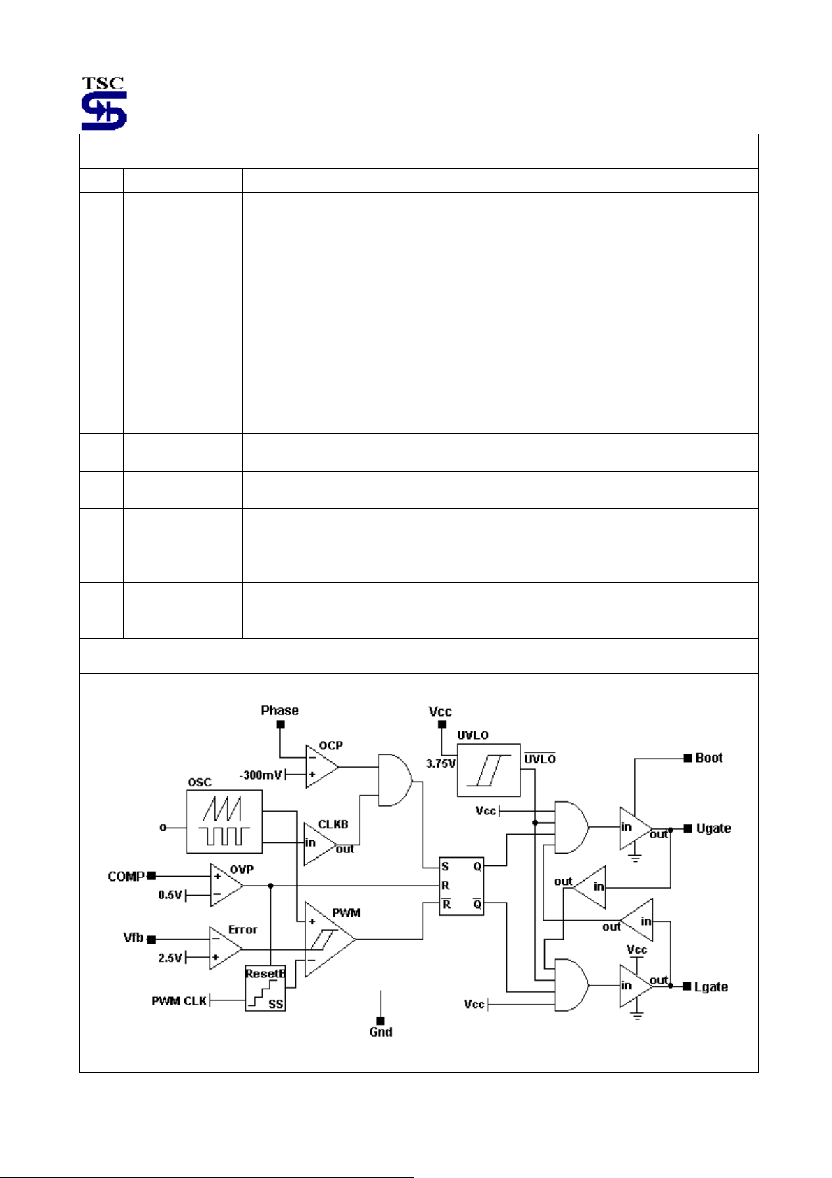
Block Diagram
TS3405 2-10 2003/12 rev. A
Electrical Characteristics (Iout= 0mA, and Tj = +25
o
C; unless otherwise specified.)
Parameter Symbol Test Conditions Min Typ Max Unit
Vcc supply current
Nominal supply IVcc
2.6 -- 3.8
mA
Power-on reset
Rising Vcc power-on reset
threshold
Vcc power-on reset threshold
POR
3.8 4.0 4.2
0.24 0.25 0.30
Hysteresis
Oscillator
Frequency F
Ramp amplitude ∆V
Vcc= 5V 250 300 340 KHz
OSC
-- 1.5 -- V
OSC
Reference
Reference voltage Tolerance
Nominal reference voltage
V
REF
-- -- 1.5
-- 0.8 -- V
Error Amplifier
DC Gain -- 82 -- dB
Gain-bandwidth product GBWP 14 -- -- MHz
Slew rate SR COMP= 10pF 4.65 8.0 9.2 V/uS
Gate Drivers
Upper gate source driver I
Upper gate sink driver I
Lower gate source driver I
Lower gate sink driver I
UGATE-SRC
UGATE-SNK
LGATE-SRC
LGATE-SNK
V
V
BOOT
VCC
= 10V, I
= 5V, I
UGATE
LGATE
= 100mA
= 100mA
-- 15 --
-- 7 --
-- 9.5 --
-- 3.5 --
Protection / Disable
OCP threshold V
Disable threshold V
V
OCP
Sweep COMP -- 0.3 -- V
DISABLE
= 5V, sweep Phase -- -300 -- mV
VCC
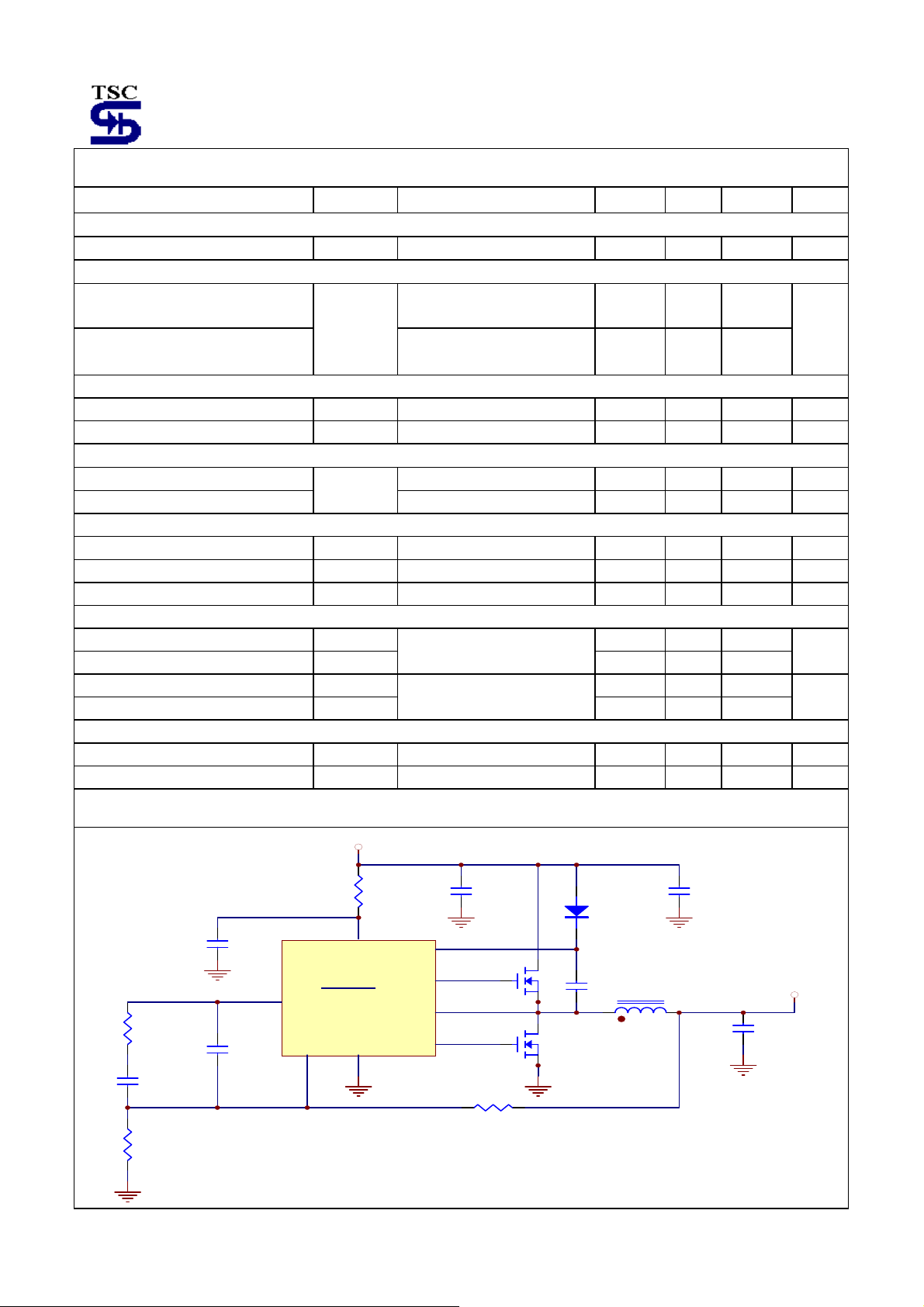
Typical Application
V
%
Ω
Ω
Vcc_5V
RF
CF
Roffset
CDCPL
C1
U1
COMP
TS3405
FB
Rfilter
Gnd Vcc
Boot
Vgate
Phase
Lgate
Cbulk
RS
Q1
Q2
Dboot
Cboot
CHF
Lout
Single Power 5V Application
TS3405 3-10 2003/12 rev. A
Vout
Cout
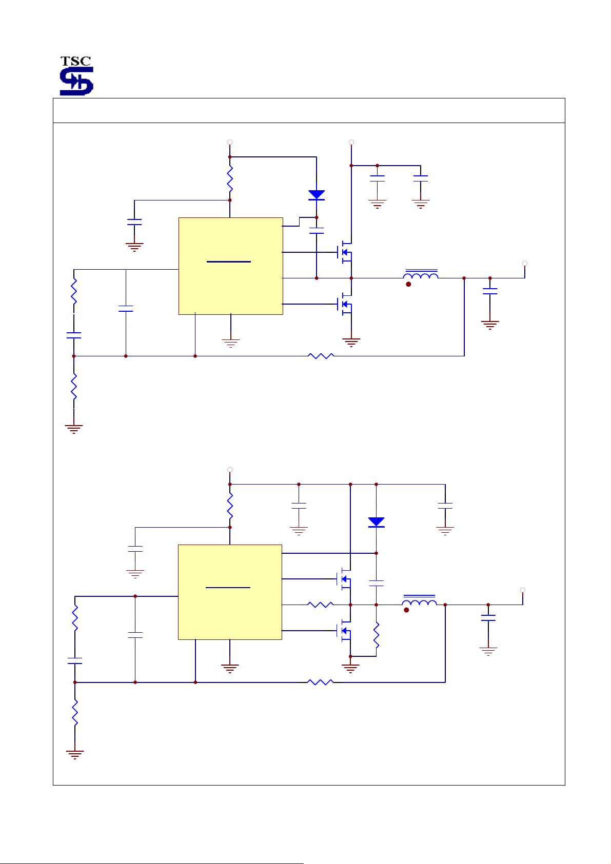
Typical Application (continued)
Vcc_12VVcc_5V
Rfilter
RF
CF
Roffset
Dboot
U1
CDCPL
C1
COMP
FB
Vcc
TS3405
Gnd
Boot
Vgate
Phase
Lgate
Cboot
Q1
Q2
RS
Single Power 5V and 12V Application
Vin
CHFCbulk
Vout
Lout
Cout
RF
CF
Roffset
CDCPL
C1
U1
COMP
TS3405
FB
Rfilter
Gnd Vcc
Boot
Vgate
Phase
Lgate
RC1
RS
Q1
Q2
Dboot
Cboot
RC2
CHFCbulk
Vout
Lout
Cout
Adjustable OCP Point Application
TS3405 4-10 2003/12 rev. A

n
Typical Application (continued)
H3
Vin_Gun
Roset
20K_5%
R2
JP1
2
1
Jumper
No. of input capacitor C13、C14 1 1 2
No. of output capacitor C8、C9、C10 1 2 3
No. of decoupling
Reference design capacitor : 1500uF(ESR=33)
Reference design decoupling capacitor : 10uF(MLCC)
43K_1%
C2
222
R4
1.5K_1%
Component Reference design
MOSFET Q1、Q2 Rds(on)<30mΩ Rds(on)<20mΩ Rds(on)<10mΩ
Inductor L1 5uF 3uF 1.6uF
capacitor
U1
C4
105
COMP
C1
821
C5A、C5B 1 1 2
H1
Vcc
TS3405
FB
R5
33
Vcc
Gnd
Boot
Vgate
Phase
Lgate
C14
C13
D1
1N4148
Q1
Q2
R1
3.3K_1%
C3
R3
56_1%
223
5A 10A 15A
C6
104
Maximum load current
C5A
L1
1.6uH/30A
C5B
C8
TP1
BNC
10uF/16V(MLCC
C10
C9
H2
Vout
C13
H4
Vout_Gu
TS3405 5-10 2003/12 rev. A

Functional Description
Start Up
The TS3405 automatically initializes upon receipt of power. The Power-On Reset (POR) function continually monitors
the bias voltage at the Vcc pin. The POR function initiates the Soft Start (SS) operation after the supply voltage
exceeds its POR threshold.
Over Current Protection (OCP)
The over current function protects the converter from a shorted output by using the lower MOSFET’s on-resistance,
Rds(on), to monitor the current. Therefore, even the power input voltage is greater than Vcc, TS3405 still can support
this. This method enhances the converter’s efficiency and reduces cost by eliminating a current sensing resistor.
The TS3405’s OCP threshold is a fixed value, -300mV, when Phase voltage is less –300mV, the next on-cycle will not
be initialized.
Over Voltage Protection (OVP)
An over voltage protection comparator is monitoring the COMP. When COMP voltage is less than 0.3V, the Soft Start
(SS) process is initiated.
Soft Start (SS)
Both POR and OVP initiate the soft start sequence after the over current set point has been sampled. Soft Start
clamps virtually the error amplifier output (COMP pin) and reference input (non-inverting terminal of the error amp) to
the internally generated Soft Start voltage. The oscillator’s triangular waveform is compared to the ramping error
amplifier voltage. This generates Phase pulses of increasing width that charge the output capacitor(s). when the
internally generated Soft Start voltage exceeds the COMP pin voltage, the output voltage is in regulation. This method
provides a rapid and controlled output voltage rise. The entire startup sequence typically takes about 5mS.
Current Sinking
The TS3405 incorporates a MOSFET shoot-through protection method which allows a converter to sink current as well
as source current. Care should be exercised when designing a converter with the TS3405 when it is known that the
converter may sink current.
When the converter is sinking current, it is behaving as a boost converter that is regulating its input voltage. This
means that the converter is boosting current into the buck converter input power, if the buck converter input power has
the same supply source which supplies the bias voltage, Vcc to the TS3405. if there is nowhere for this current to go,
such as to other distributed loads on the Vcc rail, through a voltage limiting protection device, or other methods, the
capacitance on the Vcc bus will absorb the current. This situation will allow voltage level of the Vcc rail to increase. If
the voltage level of the rail is boosted to a level that exceeds the maximum voltage rating of the TS3405, then the IC
will experience an irreversible failure and the converter will no longer be operational. Ensuring that there is a path for
the current to follow other than the capacitance on the rail will prevent this failure mode.
TS3405 6-10 2003/12 rev. A

Application Guidelines
Component Selection
Input Capacitor
Use a mix of input bypass capacitors to control the
voltage overshoot across the MOSFETs. Use small
ceramic capacitors for high frequency decoupling and
bulk capacitors to supply the current needed each time
Q1 turn on. Place the small ceramic capacitors physically
close to the MOSFETs and between the drain of high
side MOSFET (Q1) and the source of low side MOSFET
(Q2).
The important parameters for the bulk input capacitor are
the voltage rating and the RMS current rating. For
reliable operation, select the bulk capacitor with voltage
and current rating above the maximum input voltage and
largest RMS current required by the circuit. The capacitor
voltage rating should be at least 1.25 times greater than
the maximum input voltage and a voltage rating of 1.5
times is a conservative guideline. The RMS current rating
requirement for the input capacitor of a buck regulator is
approximately 1/2 the DC load current.
For a through hole design, several electrolytic capacitors
may be needed. For surface mount designs, solid
tantalum capacitors can be used, but caution must be
exercised with regard to the capacitor surge current
rating. These capacitors must be capable of handling the
surge-current at power-up. Some capacitor series
available from reputable manufacturers are surge current
tested.
MOSFET
The TS3405 requires 2 N-channel power MOSFETs.
These should be selected based upon Rds(on), gate
supply requirements, and thermal management
requirements. In high-current applications, the MOSFET
power dissipation, package selection and heatsink are
the dominant design factors. The power dissipation
includes two loss components; conduction loss and
switching loss. The conduction losses are the largest
component of power dissipation for both the upper and
the lower MOSFETs. These losses are distributed
between the two MOSFETs according to duty factor. The
switching losses seen when sourcing current will be
different from the switching losses seen when sinking
current. When sourcing current, the upper MOSFET
realizes most of the switching losses. The lower switch
realizes most of the switching losses when the converter
is sinking current (see the equations below).
These equations assume linear voltage current
transitions and do not adequately model power loss due
the reverse-recovery of the upper and lower MOSFET’s
body diode. The gate-charge losses are dissipated by the
TS3405 and do not heat the MOSFETs. However, large
gate-charge increases the switching interval, t
which
SW
increases the MOSFET switching losses. Ensure that
both MOSFETs are within their maximum junction
temperature at high ambient temperature by calculating
tempature rise according to package thermal-resistance
specifications. a separate heatsink may be necessary
depending upon MOSFET power, package type, ambient
temperature and air flow.
Losses while sourcing current:
= Io2 x Rds(on) x D + ½ Io x Vin x tSW x F
P
UPPER
P
= Io2 x Rds(on) x (1– D)
LOWER
S
Losses while sinking current:
= Io2 x Rds(on) x D
P
UPPER
P
= Io2 x Rds(on) x (1–D) + ½ Io x Vin x tSW x FS
LOWER
Where: D is the duty cycle = Vout / Vin
t
F
is the combined switch ON and OFF time
SW
is the switching frequency
S
Given the reduced available gate bias voltage (5V),
logic-level or sub-logic-level transistors should be used
for both N-MOSFETs. Caution should be exercised with
devices exhibiting very low Vgs(on) characteristics. The
shoot through protection present aboard the TS3405 may
be circumvented by there MOSFETs if they have large
parasitic impedances and /or capacitances that would
inhibit the gate of the MOSFET from being discharged
below it’s threshold level before the complementary
MOSFET is turned on.
+5V -5V
Vcc
TS3405
_
+
Gng
Dboot
VD+
Boot
Vgate
Phase
Lgate
_
CHF
Cboot
Q1
Q2
FIGURE 5、Upper Gate drive bootstrap.
Fig. 5 shows the upper gate drive (Boot pin) supplied by
a bootstrap circuit from Vcc. The boot capacitor. C
BOOT
,
develops a floating supply voltage referenced to the
Phase pin. The supply is refreshed to a voltage of Vcc
less the boot diode drop (V
) each time the lower
DP
MOSFET turns on.
TS3405 7-10 2003/12 rev. A

T
Application Guidelines (continued)
Output Inductor
The output inductor is selected to meet the output
voltage ripple requirements and minimize the converter’s
response time to the load transient. The inductor value
determines the converter’s ripple current and the ripple
voltage is a function of the ripple current. The ripple
voltage and current are approximated by the following
equations:
∆I = (Vin - Vout) / F
x L x (Vout / Vin)
S
∆Vout = ∆I x ESR
Increasing the value of inductance reduces the ripple
current and voltage. However, the large inductance
values reduce the converter’s response time to a load
transient. One of the parameters limiting the converter’s
response to a load transient is the time required to
change the inductor current. Given a sufficiently fast
control loop design, the TS3405 will provide either 0% or
100% duty cycle in response to a load transient. The
response time is the time required to slew the inductor
current from an initial current value to the transient
current level. During this interval the difference between
the inductor current and the transient current level must
be supplied by the output capacitor to minimizing the
response time can minimize the output capacitance
required.
The response time to a transient is different for the
application of load and the removal of load. The following
equations give the approximate response time interval for
application and removal of a transient load:
t
RISE
t
FALL
= (L x I
= (L x I
) / (Vin - Vout)
TRAN
) / Vout
TRAN
where:
is the transient load current step
I
TRAN
is the response time to the application of load
t
RISE
is the response time to the removal of load
t
FALL
the worst case response time can be either at the
equations at the minimum and maximum output levels for
the worst case response time.
Feedback Compensation
Fig. 6 highlights the voltage-mode control loop for a
synchronous-rectified buck converter. The output voltage
(Vout) is regulated to the reference voltage level. The
error amplifier (Error Amp) output (VE/A) is compared
with the oscillator (OSC) triangular wave to provide a
pulse-width modulated (PWM) wave with a amplitude of
Vin at the Phase node. The PWM wave is smoothed by
the output filter (Lo and Co).
The modulator transfer function is the small-signal
transfer function of Vout / V
This function is dominated
E/A.
by a DC Gain and the output filter (Lo and Co), with a
double pole break frequency at F
and a zero at F
LC
ESR.
The DC Gain of the modulator is simply the imput voltage
(Vin) divided by the peak-to-peak oscillator voltage V
OSC
.
Modulator Break Frequency Equations
FLC = 1 / 2π x √ Lo x Co
= 1 / 2π x ESR x Co
F
ESR
Compensation Break Frequency Equations
FZ = 1 / 2π x R2 x C1
= 1 / 2π x R2 x [(C1 x C2) / (C1 + C2)]
F
P1
= 1 / 2π x (R1 + R3) x C3
F
Z1
= 1 / 2π x R3 x C3
F
P2
The compensation network consists of the error amplifier
(internal to the TS3405) and the impedance networks
ZIN and ZFB. The goal of the compensation network is
to provide a closed loop transfer function with the
highest 0dB crossing frequency (f0dB) and adequate
phase margin. Phase margin is the difference between
the closed loop phase at f0dB and 180 degrees.
Vin
Driver
Lout
OSC
OSC
PWM
_
+
Driver
Phase
Vout
Co
ESR
ZFD
VE/A
_
+
ZIN
Reference
Error AMP
DETAILED COMPENSATION COMPONEN
FB
ZFD
C3
Vout
R3
R1
ZIN
C1
COMP
TS3405
C2
R2
_
+
Reference
FIGURE 6、Voltage-mode buck converter
compensation design.
TS3405 8-10 2003/12 rev. A

Application Guidelines (continued)
The equations below relate the compensation network’s
poles, zeros and gain to the components (R
and C3) in Fig. 7. Use these guidelines for locating the
C
2
, R2, R3, C1,
1
poles and zeros of the compensation network:
1. Pick Gain (R
2. Place 1
3. Place 2
4. Place 1
5. Place 2
st
nd
st
pole at the ESR zero.
nd
) for desired converter bandwidth.
2/R1
zero below filter’s double pole (~75% FLC)
zero at filter’s double pole.
pole at half the switching frequency
6. Check gain against error amplifier’s open-loop gain.
7. Estimate phase margin – repeat if necessary.
Output Capacitor Selection
An output capacitor is required to filter the output and
supply the load transient current. The filtering
requirements are a function of the switching frequency
and the ripple current. The load transient requirements
are a function of the slew rate (di/dt) and the magnitude
of the transient load current. These requirements are
generally met with a mix of capacitors and careful layout.
Modern components and loads are capable of producing
transient load rates above 1A/nS. High frequency
capacitors initially supply the transient and slow the
current load rate seen by the bulk capacitors. The bulk
filter capacitor values are generally determined by the
ESR (Effective Series Resistance) and voltage rating
requirements rather than actual capacitance
requirements.
High frequency decoupling capacitors should be placed
as close to the power pins of the load as physically
possible. Be careful not to add inductance in the circuit
board wiring that could cancel the usefulness of these
low inductance components. Consult with the
manufacturer of the load on specific decoupling
requirements.
Use only specialized low-ESR capacitors intended for
switching-regulator applications for the bulk capacitors.
The bulk capacitor’s ESR will determine the output ripple
voltage and the initial voltage drop after a high slew-rate
transient. An aluminum electrolytic capacitor’s ESR value
is related to the case size with lower ESR available in
larger case sizes. However, the equivalent Series
inductance (ESL) of these capacitors increases with case
size and can reduce the usefulness of the capacitor to
high slew-rate transient loading. Unfortunately, ESL is
not a specified parameter. Work with your capacitor
supplier and measure the capacitor’s impedance with
frequency to select a suitable component.
In most cases, multiple electrolytic capacitors of small
case size perform better than a single large case
capacitor.
Feedback Divider
The reference of TS3405 is 0.8V. the output voltage can
be set by R
and R4 as shown in Fig. 4. The equation is
1
following:
Vout = 0.8 x (1 + R
The R1 should be between 2kΩ to 5kΩ. put the R
/ R4)
1
, R4
1
and others compensation component as close to TS3405
as possible.
Shutdown
Pulling low the COMP pin can shutdown the TS3405
PWM controller. You can use a small single transistor as
switch like as JP1 shown in Fig. 4.
Compensation Break Frequency Equations
As in any high frequency switching converter, layout is
very important. Switching current from one power device
to another can generate voltage transients across the
impedances of the interconnecting bond wires and circuit
traces. Using wide, short printed circuit traces should
minimize these interconnecting impedances. The critical
components should be located as close together as
possible, using ground plane construction or single point
grounding.
To minimize the voltage overshoot, the interconnecting
wires indicated by heavy lines should be part of a ground
or power plane in a printed circuit board. Locate the
TS3405 within 3 inches of the MOSFETs. Q1 and Q2.
The circuit traces for the MOSFETs’ gate and source
connections from the TS3405 must be sized to handle up
to 1A peak current. Provide local Vcc decoupling
between Vcc and Gnd pins. Locate the capacitor, C
BOOT
as close as practical to the Boot and Phase pins. All
components used for feedback compensation should be
located as close to the IC a practical.
TS3405 9-10 2003/12 rev. A

SOP-8 Mechanical Drawing
A
SOP-8 DIMENSION
MILLIMETERS INCHES
MIN MAX MIN MAX
16
DIM
9
PB
A 4.80 5.00 0.189 0.196
B 3.80 4.00 0.150 0.157
C 1.35 1.75 0.054 0.068
1
8
D 0.35 0.49 0.014 0.019
F 0.40 1.25 0.016 0.049
G 1.27 (typ) 0.05 (typ)
G
M
C
D
K
R
F
K 0.10 0.25 0.004 0.009
M 0o 7
o
0
o
7
P 5.80 6.20 0.229 0.244
R 0.25 0.50 0.010 0.019
o
TS3405 10-10 2003/12 rev. A

WWW.ALLDATASHEET.COM
Copyright © Each Manufacturing Company.
All Datasheets cannot be modified without permission.
This datasheet has been download from :
www.AllDataSheet.com
100% Free DataSheet Search Site.
Free Download.
No Register.
Fast Search System.
www.AllDataSheet.com
 Loading...