

查询TS317L供应商
TS317L
3-Terminal Adjustable Output Positive Voltage Regulator
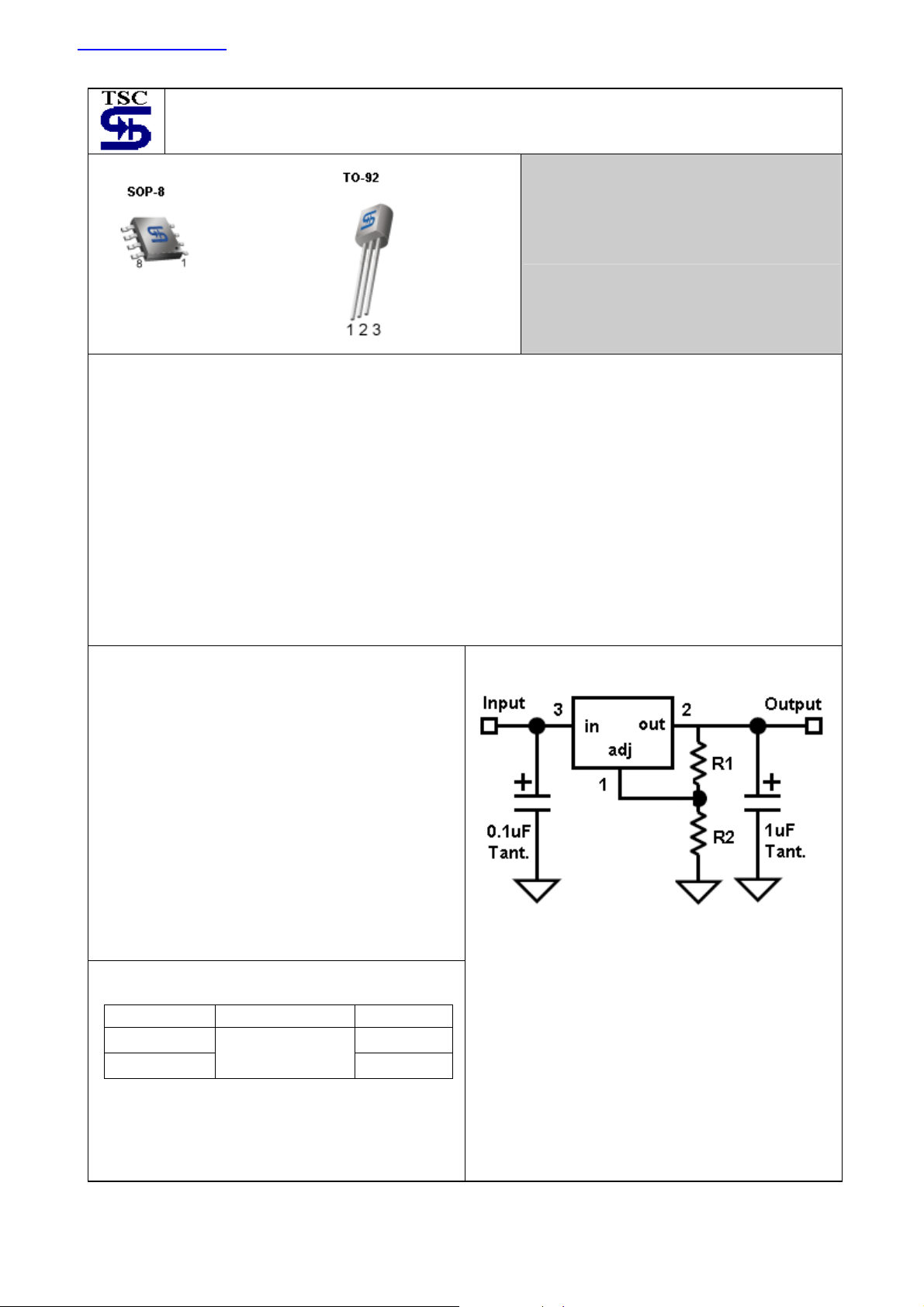
Pin assignment:
1. Input
2. Output
3. Output
4. Adjust
5. N/C
6. Output
7. Output
8. N/C
Pin assignment:
1. Adjustable
2. Output
3. Input
Output Voltage Range From
1.25V to 37V
Output Current up to 100mA
General Description
The TS317L is adjustable 3-terminal positive voltage regulator capable of supplying in excess of 100mA over an output
voltage range of 1.25 V to 37 V. This voltage regulator is exceptionally easy to use and require only two external resistors
to set the output voltage. Further, it employs internal current limiting, thermal shutdown and safe area compensation,
making it essentially blow-out proof.
Besides replacing fixed regulators, the TS317L is useful in a wide variety of other applications. Since the regulator is
“floating “ and sees only the input-to-output differential voltage, supplies of several hundred volts can be regulated as long
as the maximum input-to-output differential is not exceeded.
Also, it makes an especially simple adjustable switching regulator, a programmable output regulator, or by connecting a
fixed resistor between the adjustment and output, the TS317L can be used as a precision current regulator. Supplyies
with electronic shutdown can be achieved by clamping the adjustment terminal to ground which programs the output to
1.25V where most loads draw little current.
The TS317L is offered in 3-pin TO-92 and SOP-8 package.
Features
Output current up to 100mA
Output Adjustable between 1.25 V and 37 V
Internal Thermal Overload Protection
Internal Short-Circuit Current Limiting Constant with
Temperature
Output Transistor Safe-Area Compensation
Floating Operation for High Voltage Applications
Eliminates Stocking Many Fixed Voltages
Output voltage offered in 4% tolerance
Ordering Information
Part No. Operating Temp. Package
TS317LCS SOP-8
TS317LCT
-20 ~ +125
o
C
TO-92
Standard Application
Vout = 1.25 V * (1 + R2 / R1 ) + Iadjj * R2
Since I
associated with this term is negligible in most applications
A common ground is required between the input and the
output voltages. The input voltage must remain typically
2.0V above the output voltage even during the low point
on the Input ripple voltage.
** = Co is not needed for stability; however, it does
is controlled to less than 100 µA, the error
Adj
* = Cin is required if regulator is located an appreciable
distance from power supply filter.
improve transient response.
TS317L 1-6 2003/12 rev. A
Absolute Maximum Rating
Input Voltage Vin 40 V
Power Dissipation Pd Internal Limited W
Operating Junction Temperature Range TJ -20 ~ +125
Storage Temperature Range T
Lead Temperature (soldering 4 sec.) T
-55 ~ +150
STG
+260 oC
LEAD
o
o
Note: “Absolute maximum rating” indicated limits beyond which damage to the device may occur. Operating ratings
indicate conditions for which the device is functional, but do not guarantee specific performance limits.
Electrical Characteristics
(Tj =T
Reference voltage
(Note 4)
Line regulation
(Note 3)
Load regulation
(Note 3)
Thermal regulation Tj = 25 oC, 10 ms Pulse -- -- 0.03 0.2 %/W
Adjustment pin current Iadj -- 50 100 uA
Adjustment pin current
change
Current limit 3V ≤ VI - VO ≤ 13V
Temperature stability T
Minimum load current VI - VO ≤ 40V Imin -- 3.5 5 mA
RMS Noise, % of VO Ta =25 oC, 10H
Ripple rejection ratio Vout= 10V, f= 120Hz, Cadj= 0 -- -- 65 -- dB
Long-term stability
(Note 5)
Thermal resistance
Junction to Ambient
Notes:
1. T
2. Pmax: CS package=0.5W, CT package=0.625W,
3. Load and line regulation are specified at constant junction temperature. Changes in output voltage due to heating
4. Selected devices with tightened tolerance reference voltage available.
5. Since Long-Term Stability cannot be measured on each device before shipment, this specification is an engineering
LOW
to T
see [Note 1], Vin-Vout= 5V, Io=40mA; Pmax per [Note 2]; unless otherwise specified.)
HIGH
CHARACTERISTIC CONDITION SYMBOL MIN. TYP. MAX. UNIT
5mA ≤ Io ≤ 100mA
Vref 1.20 1.25 1.30 V
3V ≤ Vi - Vo ≤ 40V
Tj = 25 oC, 3V ≤ Vi -Vo ≤ 40V,
REGline -- 0.01 0.07 %/V
Io=20mA
o
C, 5mA ≤ IO ≤ Imax, REGload -- 0.1 1.5 %
-- 0.2 5.0 uA
∆Iadj
I
--
LIMIT
--
≤ Tj ≤ T
LOW
= 125 oC, 1000hrs S -- 0.3 1.0 %
T
HIGH
≤ f ≤ 10KHZ N -- 0.003 -- %
Z
-- 0.65 -- %
S
Rθja
--
--
200
50
180
165
--
--
--
--
o
= -20 oC, T
LOW
Tj = 25
Pd ≤ Pmax, 5mA ≤ Io ≤ Imax,
3V ≤ VI - VO ≤ 40V
VI - VO = 40V
Tj
CT package 0.4” leads
CS package
= + 125 oC
HIGH
effects must be taken into account separately. Pulse testing with low duty cycle is used.
estimate of average stability from lot to lot.
C
C
mA
C/W
TS317L 2-6 2003/12 rev. A

Application Information
Basic Circuit Operation
The TS317L is a 3-terminal floating regulator. In
operation, the TS317L develops and maintains a
nominal 1.25V reference (Vref) between its output and
adjustment terminals. This reference voltage is
converted to a programming current (Iprog.) by R
Figure 17), and this constant current flows through R
to ground. The regulated output voltage is given by:
Vout = Vref ( 1 + R2 / R1 ) + Iadj * R2
Since the current from the adjustment terminal (Iadj)
represents an error term in the equation, the TS317L
was designed to control Iadj to less than 100uA and
keep it constant. To do this, all quiescent operating
current is returned to the output terminal. This imposes
the requirement for a minimum load current. If the load
current is less than this minimum, the output voltage
will rise.
Since the TS317L is a floating regulator, it is only the
voltage differential across the circuit which is important
to performance, and operation at high voltages with
respect to ground is possible.
(see
1
2
If the set resistor is connected near the load the
effective line resistance will be 0.05Ω (1+ R2/R1) or in
this case, 11.5 times worse.
Figure 6 shows the effect of resistance between the
regulator and 240Ω set resistor.
With the TO-92 package, it is easy to minimize the
resistance from the case of the set resistor, by using
two separate leads to the output pin. The ground of R2
can be returned near the ground of the load to provide
remote ground sensing and improve load regulation.
Figure 2. Regulator with line resistance in
output lead
Figure 1. basic circuit configuration
Load Regulation
The TS317L is capable of providing extremely good
load regulation, but a few precautions are needed to
obtain maximum performance. The current set resistor
connected between the adjustment therminal and the
output terminal (usually 240Ω) should be tied directly to
the output of the regulator rather than near the load.
This eliminates line drops from appearing effectively in
series with the reference and degrading regulation. For
example, a 15V regulator with 0.05Ω resistance
between the regulator and load will have a load
regulation due to line resistance of 0.05Ω x Io.
External Capacitor
An input bypass capacitor is recommended in case the
regulator is more than 6 inches away from the usual
large filter capacitor. A 0.1µF disc or 1µF tantalum
input bypass capacitor (Cin) is recommended to reduce
the sensitivity to input line impedance.
The adjustment terminal may be bypassed to ground to
improve ripple rejection and noice. This capacitor
(Cadj) prevents ripple from being amplified as the
output voltage is increased. With a 10uF bypass
capacitor 80dB ripple rejection is obtainable at any
output level. Increased over 10uF do not appreciably
improve the ripple rejection at frequencies above
120Hz. If the bypass capacitor is used, it is sometimes
necessary to include protection diodes to prevent the
capacitor from discharging through internal low current
paths and damaging the device.
In general, the best type of capacitors to use is solid
tantalum. Solid tantalum capacitors have low
impedance even at high frequencies. Depending upon
capacitor construction, it takes about 25uF in aluminum
electrolytic to equal 1uF solid tantalum at high
frequencies. Ceramic capacitors are also good at high
frequencies; but some types have a large
TS317L 3-6 2003/12 rev. A

Application Information (continued)
decrease in capacitance at frequencies around
0.5MHz. for this reason, a 0.01uF disc may seem to
work better than a 0.1uF disc as a bypass.
Although the TS317L is stable with no output
capacitance, like any feedback circuit, certain values of
external capacitance can cause excessive ringing. This
occurs with values between 50pF and 5000pF. A 1uµF
solid tantalum (or 25uF aluminum electrolytic) on the
output swamps this effect and insures stability.
Thermal Regulation
When power is dissipated in an IC, a temperature
gradient occurs across the IC chip affecting the
individual IC circuit components. With an IC regulator,
this gradient can be especially severe since power
dissipation is large. Thermal regulation is the effect of
these temperature gradients on output voltage (in
percentage output change) per watt of power change in
a specified time. Thermal regulation error is
independent of electrical regulation of temperature
coefficient, and occurs within 5ms to 50ms after a
change in power dissipation. Thermal regulation
depends on IC layout as well as electrical design. The
thermal regulation of a voltage regulator is defined as
the percentage change of Vout, per watt, within the first
10ms after a step of power is applied. The TS317L
specification is 0.2%/W, maximum.
TS317L’s output changes only 7mV (or 0.07% of Vout=
-10V) when a 1W pulse is applied for 10ms. This
performance is thus well inside the specification limit of
0.2%/W x 1W = 0.2% maximum. When the 1W pulse is
ended, the thermal regulation again shows a 7mV
change as the gradients across the TS317L chip die
out. Note that the load regulation error of about 14mV
(0.14%) is additional to the thermal regulation error.
Discharge into the output of the regulator. The
discharge current depends on the value of the
capacitor, the output voltage of the regulator, and the
rate of decrease of Vin. In the TS317L, this discharge
path is through a large junction that is able to sustain a
2A surge with no problem. this is not true of other types
of positive regulators. For output capacitors of 25uF or
less, the TS317L’s ballast resistors and output
structure limit the peak current to a low enough level so
that there is no need to use a protection diode.
The bypass capacitor on the adjustment terminal can
discharge through a low current junction. Discharge
occurs when either the input or output is shorted.
Internal to the TS317L is a 50Ω resistor which limits the
peak discharge current. No protection is needed for
output voltages of 25V or less and 10uF capacitance.
Figure 3 shows an TS317L with protection diodes
included for use with outputs greater than 25V and high
values of output capacitance.
F
igure 3. regulator with protection diode
Protection Diode
When external capacitors are used with any I.C.
regulator it is sometimes necessary to add protection
diodes to prevent the capacitors from discharging
through low current points into the regulator. Most
10uF capacitors have low enough internal series
resistance to deliver 20A spikes when shorted.
Although the surge is short, these is enough energy to
damage parts of the IC.
When an output capacitor is connected to a regulator
and the input is shorted, the output capacitor will
TS317L 4-6 2003/12 rev. A

Typical Application
Digitally selected outputs
Adjustable regulator with improved
Ripple rejection
High gain amplifier
Slow turn-on 15V regulator
Adjustable current limiter
Precision current limiter
5V logic regulator with electronic shutdown
Current limited 6V charger
TS317L 5-6 2003/12 rev. A

TO-92 Mechanical Drawing
A
TO-92 DIMENSION
DIM
B
C
E F
A 4.30 4.70 0.169 0.185
B 4.30 4.70 0.169 0.185
C 14.30(typ) 0.563(typ)
D 0.43 0.49 0.017 0.019
E 2.19 2.81 0.086 0.111
F 3.30 3.70 0.130 0.146
G 2.42 2.66 0.095 0.105
H 0.37 0.43 0.015 0.017
MILLIMETERS INCHES
MIN MAX MIN MAX
16
1
H
G
D
SOP-8 Mechanical Drawing
A
SOP-8 DIMENSION
DIM
9
PB
8
G
M
C
D
K
R
F
A 4.80 5.00 0.189 0.196
B 3.80 4.00 0.150 0.157
C 1.35 1.75 0.054 0.068
D 0.35 0.49 0.014 0.019
F 0.40 1.25 0.016 0.049
G 1.27 (typ) 0.05 (typ)
K 0.10 0.25 0.004 0.009
M 0o 7
P 5.80 6.20 0.229 0.244
R 0.25 0.50 0.010 0.019
MILLIMETERS INCHES
MIN MAX MIN MAX
o
0
o
7
o
TS317L 6-6 2003/12 rev. A
 Loading...