

查询TS317供应商
TS317
3-Terminal Adjustable Output Positive Voltage Regulator
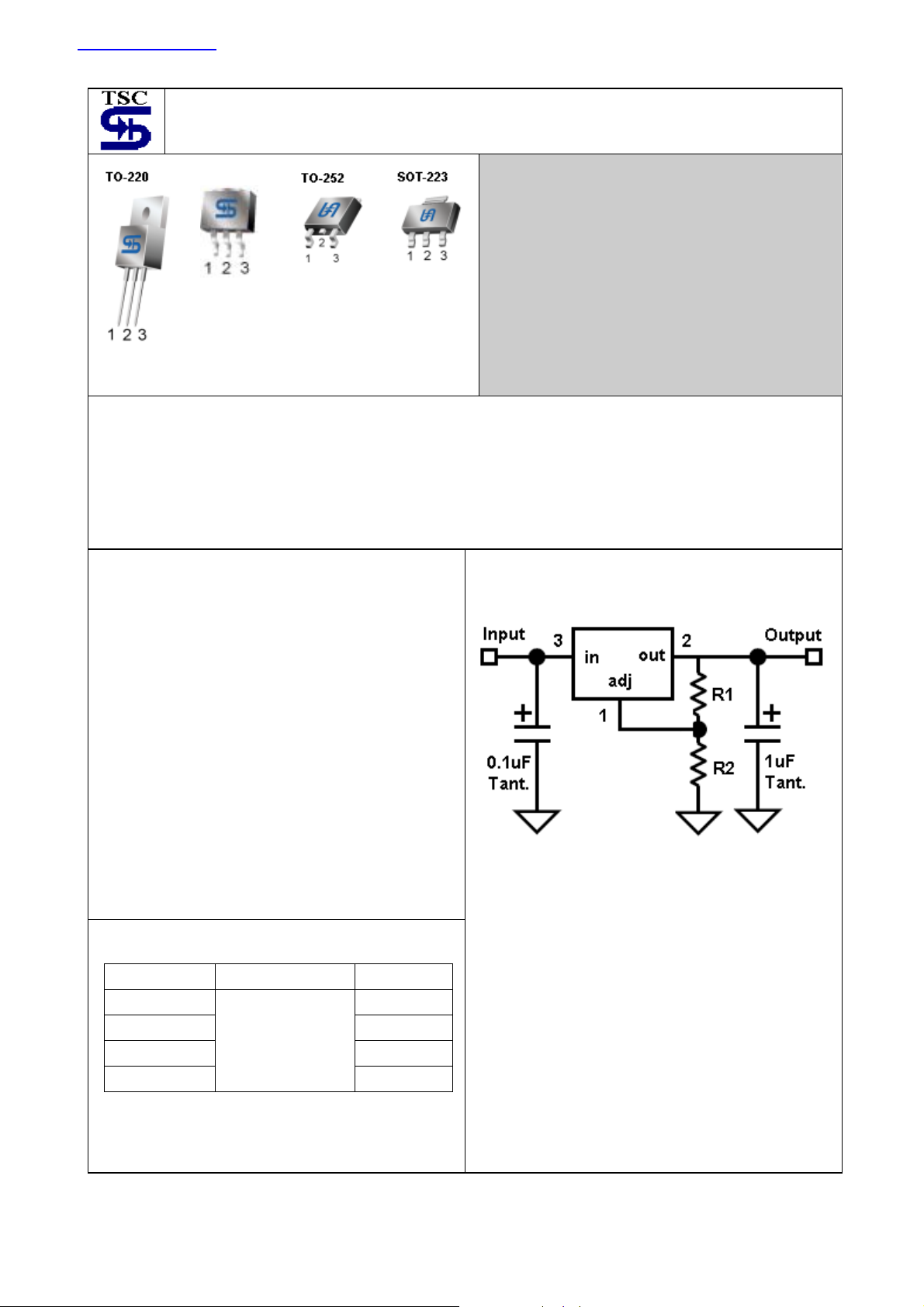
TO-263
Pin assignment:
1. Adjustable
2. Output
3. Input
(Heatsink surface connected to pin 2)
Output Voltage Range From
1.25V to 37V
Output Current up to 1.5A
General Description
The TS317 is adjustable 3-terminal positive voltage regulator capable of supplying in excess of 1.5A over an output
voltage range of 1.25 V to 37 V. This voltage regulator is exceptionally easy to use and require only two external resistors
to set the output voltage. Further, it employs internal current limiting, thermal shutdown and safe area compensation,
making it essentially blow-out proof.
The TS317 is offered in 3-pin TO-220, TO-263, TO-252 and SOT-223 package.
Features
Standard Application
Output current up to 1.5A
* TO-220/TO-263 for 1.5A
* TO-252/SOT-223 for 500mA
Output Adjustable between 1.25 V and 37 V
Internal Thermal Overload Protection
Internal Short-Circuit Current Limiting Constant with
Temperature
Output Transistor Safe-Area Compensation
Floating Operation for High Voltage Applications
Eliminates Stocking Many Fixed Voltages
Output voltage offered in 4% tolerance
Ordering Information
Part No. Operating Temp. Package
TS317CZ TO-220
TS317CM TO-263
TS317CP TO-252
TS317CW
-20 ~ +150oC
SOT-223
Vout = 1.25 V * (1 + R2 / R1 ) + Iadjj * R2
Since I
associated with this term is negligible in most applications
A common ground is required between the input and the
output voltages. The input voltage must remain typically
2.0V above the output voltage even during the low point
on the Input ripple voltage.
** = Co is not needed for stability; however, it does
is controlled to less than 100 µA, the error
Adj
* = Cin is required if regulator is located an appreciable
distance from power supply filter.
improve transient response.
TS317 1-8 2003/12 rev. D
Absolute Maximum Rating
Input Voltage Vin 40 V
Power Dissipation Pd Internal Limited W
Operating Junction Temperature Range TJ -20 ~ +150
Storage Temperature Range T
-65 ~ +150
STG
o
C
o
C
Electrical Characteristics
(VI -VO = 5.0 V, Io=500mA for TO-220/TO-263 packages, Io=200mA for TO-252/SOT-223 package;
Tj =T
LOW
to T
see [Note 1]; Pmax per [Note 2]; unless otherwise specified.)
HIGH
CHARACTERISTIC FIGURE SYMBOL MIN. TYP. MAX. UNIT
Reference voltage (Note 4) Pd ≤ Pmax,
10mA ≤ Io ≤ Imax, 3.0 V ≤ Vi
- Vo ≤ 40 V
Line regulation (Note 3)
o
Ta = 25
C, 3.0 V ≤ Vi -Vo ≤ 40 V
Load regulation (Note 3)
o
Ta = 25
C, 10mA ≤ IO ≤ Imax, VO ≤ 5.0
≥ 5.0
V
O
Thermal regulation
o
Ta = 25
C, 20 ms Pulse
3
1
2 REGload
Vref
REGline
1.20
--
--
--
--
1.25
0.01
5.0
0.1
0.03
1.30
0.07
%/V
25
0.5
mV
%V
0.07 %Vo/W
Adjustment pin current 3 Iadj -- 50 100 uA
Adjustment pin current change, Pd ≤ Pmax,
10mA ≤ Io ≤ Imax, 2.5V ≤ V
- VO ≤ 40V
I
Maximum output current
Pd ≤ Pmax, (Vin-Vout) ≤15V
CZ, CM Package
CP, CW Package
Temperature stability (T
LOW
≤ Tj ≤ T
) 3 TS -- 1 -- %
HIGH
Minimum load current to maintain regulation
- VO = 40 V)
(V
I
RMS Noise, % of V
Ta =25 oC, 10H
Long-term stability (Note 5), Tj = T
o
Ta =25
C for endpoint measurements ,1000hrs
O,
≤ f ≤ 10KHZ
Z
HIGH
1.2
3 Imin -- 3.5 10 mA
-- N -- 0.003 -- %
3 S -- 0.3 1.0 %
∆Iadj
Imax
-- 0.2 5.0 uA
1.5
0.5
Notes:
1. T
= -20 oC, T
LOW
= + 150oC
HIGH
2. Pmax: CZ package=20W, CM package=3W, CP package=1.5W, CW package=0.8W,
3. Load and line regulation are specified at constant junction temperature. Changes in V
due to heating effects must
O
be taken into account separately. Pulse testing with low duty cycle is used.
4. Selected devices with tightened tolerance reference voltage available.
5. Since Long-Term Stability cannot be measured on each device before shipment, this specification is an engineering
estimate of average stability from lot to lot.
6. Cadj, when used, is connected between the adjustment pin and ground.
V
A
TS317 2-8 2003/12 rev. D
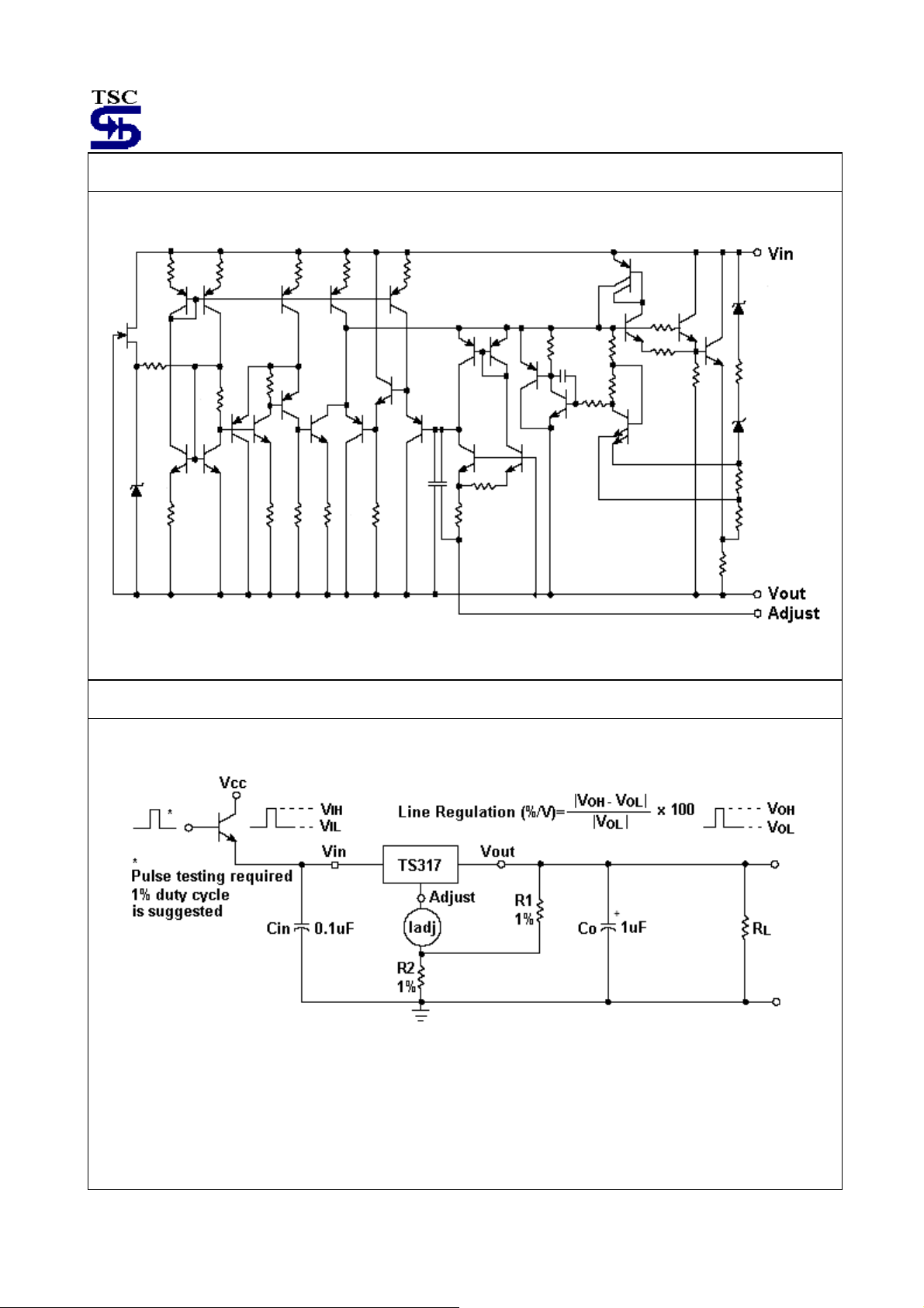
Block Diagram
Test Circuit
Figure 1. line regulation and ∆Iadj/line test circuit
TS317 3-8 2003/12 rev. D

Test Circuit
Figure 2. load regulation and ∆Iadj/line test circuit
Figure 3. standard test circuit
Figure 4. ripple rejection test circuit
TS317 4-8 2003/12 rev. D

Application Information
Basic Circuit Operation
The TS317 is a 3-terminal floating regulator. In
operation, the TS317 develops and maintains a
nominal 1.25V reference (Vref) between its output and
adjustment terminals. This reference voltage is
converted to a programming current (Iprog.) by R
Figure 17), and this constant current flows through R
to ground. The regulated output voltage is given by:
Vout = Vref ( 1 + R2 / R1 ) + Iadj * R2
Since the current from the adjustment terminal (Iadj)
represents an error term in the equation, the TS317
was designed to control Iadj to less than 100uA and
keep it constant. To do this, all quiescent operating
current is returned to the output terminal. This imposes
the requirement for a minimum load current. If the load
current is less than this minimum, the output voltage
will rise.
Since the TS317 is a floating regulator, it is only the
voltage differential across the circuit which is important
to performance, and operation at high voltages with
respect to ground is possible.
(see
1
2
External Capacitor
A 0.1µF disc or 1µF tantalum input bypass capacitor
(Cin) is recommended to reduce the sensitivity to input
line impedance.
The adjustment terminal may be bypassed to ground to
improve ripple rejection. This capacitor (Cadj) prevents
ripple from being amplified as the output voltage is
rejection about 15dB at 120 H
Although the TS317 is stable with no output
capacitance, like any feedback circuit, certain values of
external capacitance can cause excessive ringing. An
output increased. A 10uµF capacitor should improve
ripple capacitance (Co) in the form of a 1uF tantalum
or 25uF aluminum electrolytic capacitor on the output
swamps this effect and insures stability.
in a 10V application.
Z
Protection Diode
When external capacitors are used with any I.C.
regulator it is sometimes necessary to add protection
diodes to prevent the capacitors from discharging
through low current points into the regulator.
Figure 18 shows the TS317 with the recommended
protection diodes for output voltages in excess of 25 V
or high capacitance values (Co > 25uF, Cadj > 10uF).
Diode D1 prevents Co from discharging thru the I.C.
during an input short circuit. Diode D2 protects against
capacitor C
output short circuit. The combination of diodes D1
D2 prevents C
during an input short circuit.
discharging through the I.C. during an
ADJ
from discharging through the I.C.
ADJ
and
Figure 5. basic circuit configuration
Load Regulation
The TS317 is capable of providing extremely good load
regulation, but a few precautions are needed to obtain
maximum performance. For best performance, the
programming resistor (R1) should be connected as
close to the regulator as possible to minimize line
drops which effectively appear in series with the
reference, thereby degrading regulation. The ground
end of R2 can be returned near the load ground to
provide remote ground sensing and improve load
regulation.
TS317 5-8 2003/12 rev. D
Figure 6. voltage regulator with
protection diode

Application Information
Figure 7. “LABORATORY” power supply with adjustable current limit and output voltage
Figure 8. adjustable current limiter
Figure 9. 5V electronic shutdown regulator
Figure10. slow turn-on regulator
TS317 6-8 2003/12 rev. D
Figure 11. current regulator

TO-220 Mechanical Drawing
O
K
L
DIM
A 10.000 10.500 0.394 0.413
B 3.240 4.440 0.128 0.175
C 2.440 2.940 0.096 0.116
D - 6.350 - 0.250
E 0.381 1.106 0.015 0.040
F 2.345 2.715 0.092 0.058
M
N
G 4.690 5.430 0.092 0.107
H 12.700 14.732 0.500 0.581
I 8.382 9.017 0.330 0.355
J 14.224 16.510 0.560 0.650
K 3.556 4.826 0.140 0.190
L 0.508 1.397 0.020 0.055
M 27.700 29.620 1.060 1.230
N 2.032 2.921 0.080 0.115
O 0.255 0.610 0.010 0.024
P 5.842 6.858 0.230 0.270
TO-220 DIMENSION
MILLIMETERS INCHES
MIN MAX MIN MAX
A
B
C
P
J
I
D
H
F
E
G
TO-263 Mechanical Drawing
TO-263 DIMENSION
A
E
DIM
F
A 10.000 10.500 0.394 0.413
B 14.605 15.875 0.575 0.625
B
I
H
C
D
G
C 0.508 0.991 0.020 0.039
D 2.420 2.660 0.095 0.105
E 4.064 4.830 0.160 0.190
F 1.118 1.400 0.045 0.055
G 0.450 0.730 0.018 0.029
H 8.280 8.800 0.325 0.346
I 1.140 1.400 0.044 0.055
J 1.480 1.520 0.058 0.060
MILLIMETERS INCHES
MIN MAX MIN MAX
TS317 7-8 2003/12 rev. D

TO-252 Mechanical Drawing
J
A
B
D
C
E
F
I
G
H
DIM
A 6.570 6.840 0.259 0.269
B 9.250 10.400 0.364 0.409
C 0.550 0.700 0.022 0.028
D 2.560 2.670 0.101 0.105
E 2.300 2.390 0.090 0.094
F 0.490 0.570 0.019 0.022
G 1.460 1.580 0.057 0.062
H 0.520 0.570 0.020 0.022
I 5.340 5.550 0.210 0.219
J 1.460 1.640 0.057 0.065
TO-252 DIMENSION
MILLIMETERS INCHES
MIN MAX MIN MAX
SOT-223 Mechanical Drawing
A
SOT-223 DIMENSION
B
H
F
G
E
C
D
I
J
K
DIM
A 6.350 6.850 0.250 0.270
B 2.900 3.100 0.114 0.122
C 3.450 3.750 0.136 0.148
D 0.595 0.635 0.023 0.025
E 4.550 4.650 0.179 0.183
F 2.250 2.350 0.088 0.093
G 0.835 1.035 0.032 0.041
H 6.700 7.300 0.263 0.287
I 0.250 0.355 0.010 0.014
J 10° 16° 10° 16°
K 1.550 1.800 0.061 0.071
MILLIMETERS INCHES
MIN MAX MIN MAX
TS317 8-8 2003/12 rev. D
 Loading...