


TTP/TDP 243/342
THERMAL TRANSFER / DIRECT THERMAL
BAR CODE PRINTER
SERVICE
MANUAL

TTP-243 Bar Code Printer
Service Manua
l
Table Of Contents
1. FUNDAMENTALS ABOUT THE SYSTEM ........................................................................ 1
1.1 Features of the TTP/TDP-243 Series........................................................................... 1
1.2 Model Naming Syntax..................................................................................................1
1.3 Overview ......................................................................................................................2
1.3.1 Front View............................................................................................................. 2
1.3.2 Rear View............................................................................................................. 3
1.4 Basic Specifications ..................................................................................................... 4
1.5 Effective Print Area....................................................................................................... 6
1.6 Available Bar Codes..................................................................................................... 6
1.7 Various Sensors........................................................................................................... 7
2. SUPPLY SPECIFICATIONS............................................................................................... 9
2.1 Types of Paper............................................................................................................. 9
2.2 Specifications...............................................................................................................9
2.3 Ribbon Sizes and Shapes.......................................................................................... 11
3. ELECTRONICS ................................................................................................................ 12
3.1 Circuit Description...................................................................................................... 12
3.2 MCU Pin Description.................................................................................................. 15
3.3 Reset Circuit...............................................................................................................17
3.4 Memory System ......................................................................................................... 17
3.5 Connector Circuit Diagram......................................................................................... 18
3.6 Real-Time Clock Circuit.............................................................................................. 20
3.7 Decode Circuit............................................................................................................ 21
3.8 Thermal Head Drive/ Protection and History Control Circuit......................................23
3.9 24V/5V Converter Circuit............................................................................................ 24
3.10 Stepping Motor And DC Motor Driver/ Protection Circuit......................................... 25
3.11 Communication (Serial & Parallel Port) Circuit......................................................... 27
3.12 Cutter Drive Circuit................................................................................................... 28
3.13 Mainboard Replacement.......................................................................................... 29
i

TTP-243 Bar Code Printer
Service Manua
l
3.14 Flash memory Replacement .................................................................................... 33
3.15 Cutter, DC Motor, Stepping Motor Driver IC Replacement ...................................... 34
4. MECHANISM.................................................................................................................... 35
4.1 Cutter Installation ....................................................................................................... 35
4.2 Print Head Replacement............................................................................................ 36
4.3 DC Motor Replacement.............................................................................................. 38
4.4 Ribbon Rewind Spindle Encoder Replacement ......................................................... 39
4.5 Felt Fabric Replacement............................................................................................ 40
4.6 Stepping Motor Replacement..................................................................................... 42
4.7 Black Mark Sensor / Gap Sensor (Receiver) Replacement....................................... 43
4.8 Ribbon Sensor (Receiver) Replacement.................................................................... 44
4.9 Ribbon Sensor (Transmitter) / Gap Sensor (Transmitter) Replacement....................46
4.10 Platen Replacement................................................................................................. 47
4.11 Parts List .................................................................................................................. 50
5. TROUBLE SHOOTING..................................................................................................... 60
5.1 Error Messages.......................................................................................................... 60
5.2 Trouble Shooting........................................................................................................ 61
5.3 Calibrate the Gap Register......................................................................................... 62
5.4 Self-test......................................................................................................................62
5.5 Ram Clear.................................................................................................................. 62
5.6 Diagnosis Operation Procedure................................................................................. 62
5.7 Testing Sensors ......................................................................................................... 63
5.8 Cleaning the Print Head............................................................................................. 65
ii

TTP-243 Bar Code Printer
Service Manua
l
1. FUNDAMENTALS ABOUT THE SYSTEM
1.1 Features of the TTP/TDP-243 Series
1. TTP-243 bar code printer prints bar codes, characters, logos, on various types of labels and
tickets by direct thermal or thermal transfer printing.
2 TTP-243 adopts a “BASIC-like” high level programming language to help users programme
the desired label forms with ease.
3. TTP-243 bar code printer can be connected to a personal computer or an optional LCD
keyboard to execute the programs downloaded in the printer’s memory. The printer is
equipped with the following standard devices: black mark sensor, peel off module and real
time clock
4. TTP-243 bar code printer provides a selection of optional features, including cutter module,
memory module, portable LCD keyboard, etc.
5. The user friendly “Label Today!” package is bundled with TTP-243.
1.2 Model Naming Syntax
T T P – 2 4 3
(1) (2) (3) (4)
(1) Print method:
TTP – Thermal Transfer Printing
TDP – Thermal Direct Printing
(2) Resolution of print head (DPI)
(3) Maximum print width (Inch)
(4) Maximum print speed (Inch/Sec)
1
TTP-243 Bar Code Printer
Service Manua
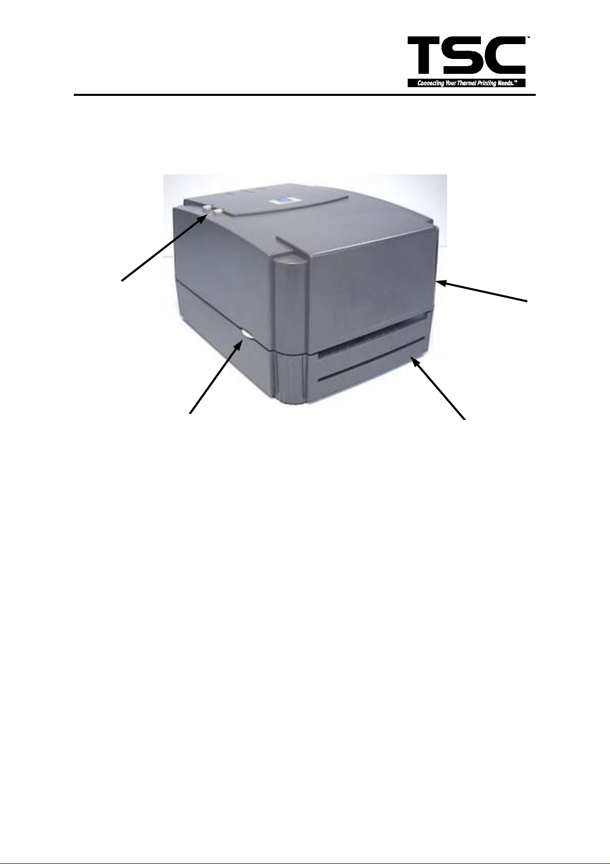
1.3 Overview
1.3.1 Front View
Operation Panel
l
Top Cover
Cover Release Button
Fig. 1.1 Front View of TTP-243
Note: The one difference between TTP model and TDP model is the ribbon
mechanism.
Front Panel
2
TTP-243 Bar Code Printer
Service Manua
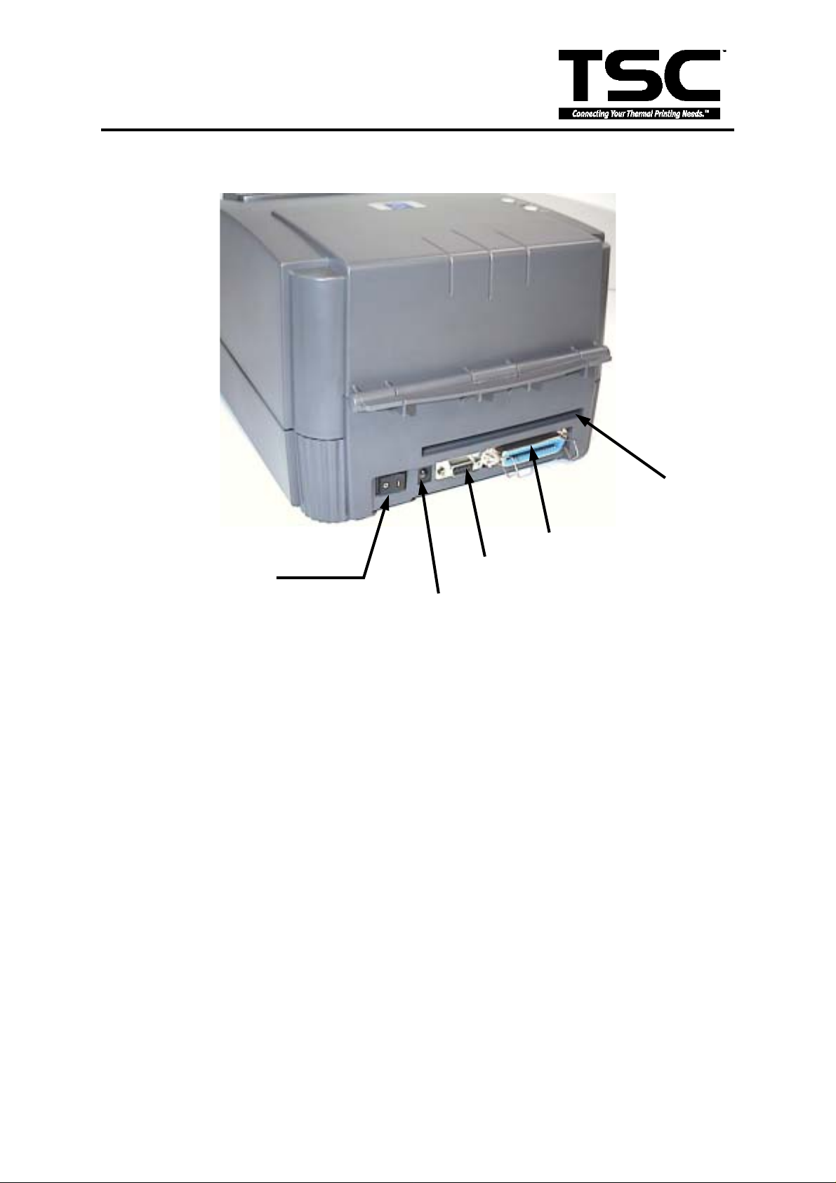
1.3.2 Rear View
Power
Switch
l
-
DC Power Jack
Label
Entrance
(External
Mount Use)
Centronics Interface
Fig. 1.2 Rear view of TTP-243
3

TTP-243 Bar Code Printer
Service Manua
l
1.4 Basic Specifications
Thermal transfer and direct thermal printing
High dot density printing (203 dots/inch)
Selectable print speeds at 1.5”, 2.0” or 3.0” per second
Supports parallel and serial interface
Maximum media width up to 4.4” (114 mm)
Adjustable label edge guide
International character sets
Print area is 4.09”W x 90”L (without any file downloaded in the printer memory)
User selectable bar code ratios and heights
Prints on labels or tickets
Equipped with black mark sensor
Equipped with Real Time Clock
Comes with self-peeling function
Buzzer provided to warn of possible errors
Label stock and thermal transfer ribbon are easy to install
Internal label print counter
Self test and hex dump mode
Downloadable fonts from label design software
Electronics/Communication Specifications
Electrical
CPU: MITSUBISHI M37720S1BFP
TPH: ROHM 4” KF-2004-GC17B
Stepping Motor: Mitsumi
DC Motor: DC24V
Memory:
─DRAM: MOSEL 2 Mb.
─Flash: ATMEL 1 Mb
Adapter 100~240VAC±10%, 50~60Hz
Regulations: CE, FCC, UL, CUL, TÜV-GS, CNS
Communications Interface:
Serial port: RS-232C (DB-9) at 2400, 4800, 9600 or 19200 baud rate
─Word Length: 7 or 8 data bits, 1 or 2 stop bits, selectable parity
─Handshaking: XON/XOFF and DSR/DTR
Parallel port: Standard parallel interface
Input Buffer: 60KB
4
TTP-243 Bar Code Printer
Service Manua
l
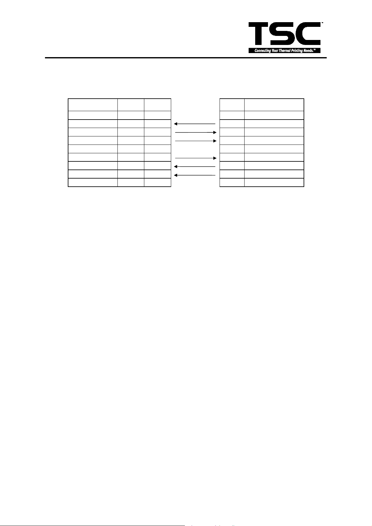
RS-232 Interface Pin Configuration:
Host Function 9 Pin 25 Pin 9 Pin Printer Function
RxD
TxD
DTR 4 20 4 DSR
GND 5 7 5 GND
DSR 6 6 6 RDY
RTS 7 4 7 N/C
CTS 8 5 8 RDY
9 +5V
2
3 2
3
2 TxD
1
3
+5V
RxD
5
TTP-243 Bar Code Printer
Service Manua
l
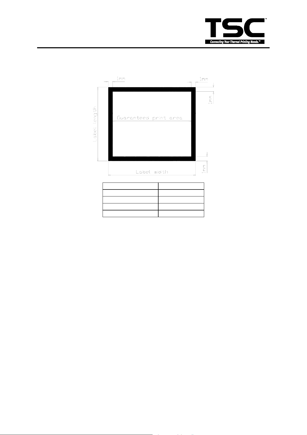
1.5 Effective Print Area
Label/Ticket Length
Effective Print Length 10mm~2284mm
Label/Ticket Width 25mm~103mm
Effective Print Width 23mm~101mm
No Print Area 1mm
12mm~2286mm
1.6 Available Bar Codes
Code 39
Code 93
Code 128 UCC
Code 128, Subsets A, B, and C
Codabar
Interleaved 2 of 5
EAN-8, EAN-13, EAN-128
UPC-A, UPC-E
EAN and UPC with 2 or 5 digits add-on
UPC Shipping container code
Postnet
Maxicode
PDF-417
DataMatrix
6
TTP-243 Bar Code Printer
Service Manua
l
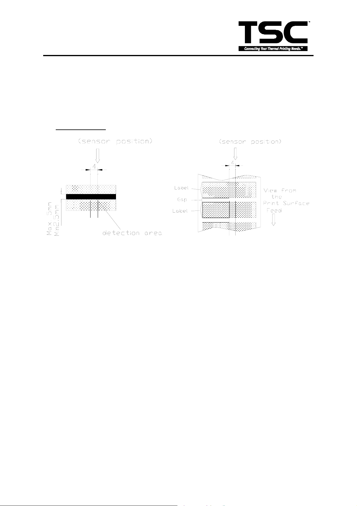
1.7 Various Sensors
(1) Feed Gap Sensor
The feed gap sensor detects a label gap to locate the starting print position of the next
label. The sensor is mounted 4 mm off the center line of the main mechanism.
.
In case of Label
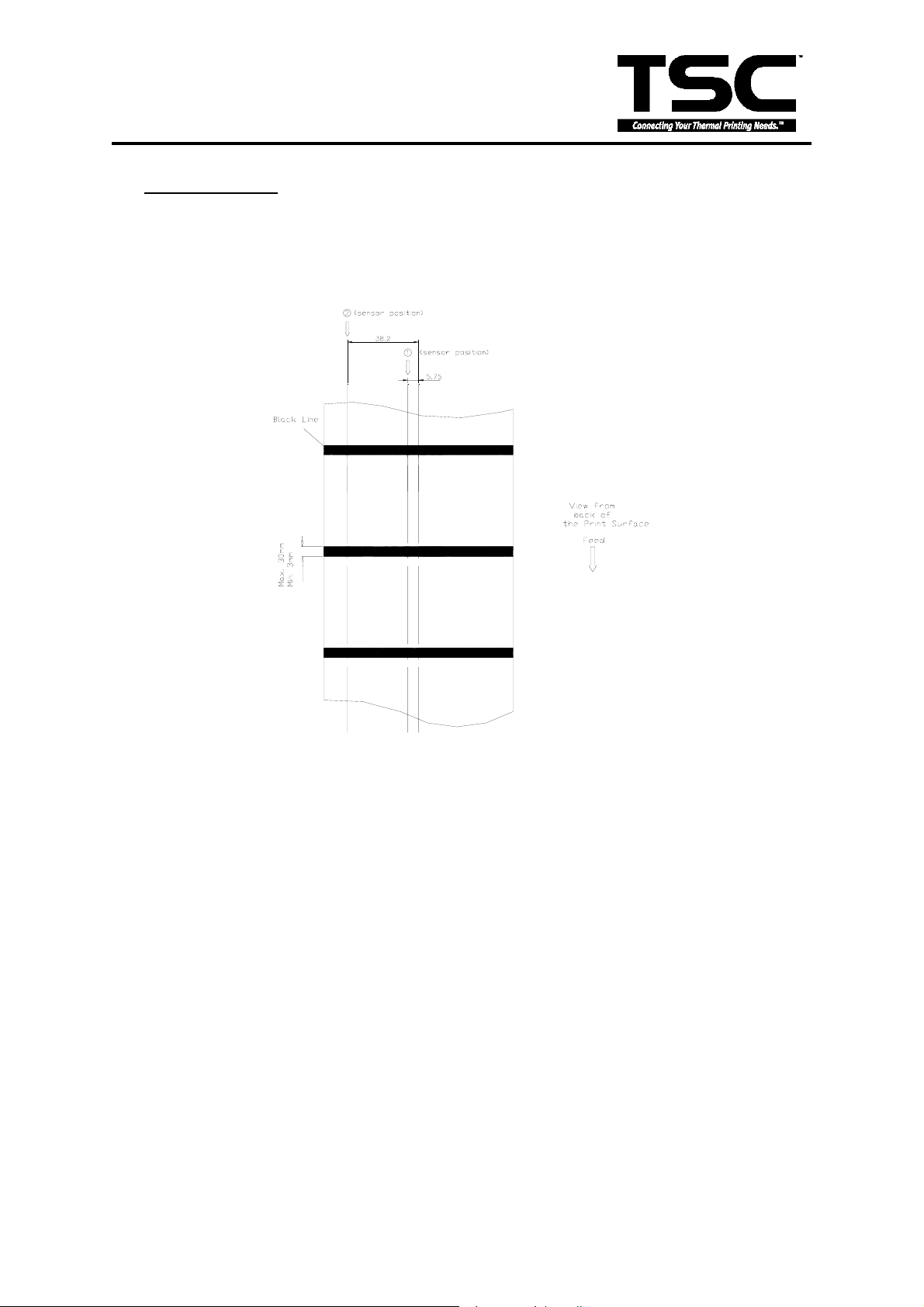
(2) Black Mark Sensor
The black mark sensor locates the position of label by emitting infrared rays onto the
black mark at the back of the ticket. The sensor is mounted 5.75 mm off the center line of
the ticket roll width on the mechanism.
7
TTP-243 Bar Code Printer
Service Manua
In case of Ticket
The default sensor position is (1) as shown on the figure below. To change to the (2)
position, the customer should notify the manufacturer in advance. There can be only
one position for the sensor. Once the sensor position is agreed upon, it can not be
changed afterwards.
l
(3) Ribbon End Sensor
The sensor detects the end portion of the ribbon. The ribbon end must be transparent.
(4) Label End Sensor
The sensor detects the end portion of the label.
(5) Peel off Sensor
The sensor detects the backing paper of a label.
(6) Ribbon encoder
The encoder is used to detect if the ribbon is broken.
8

TTP-243 Bar Code Printer
Service Manua
l
2. SUPPLY SPECIFICATIONS
2.1 Types of Paper
Two types of media are available for TTP-243: label and ticket.
In TTP-243, there are two types of sensors for paper: gap sensor and black mark
sensor.
Label and ticket can be further classified into direct thermal type or thermal transfer
type.
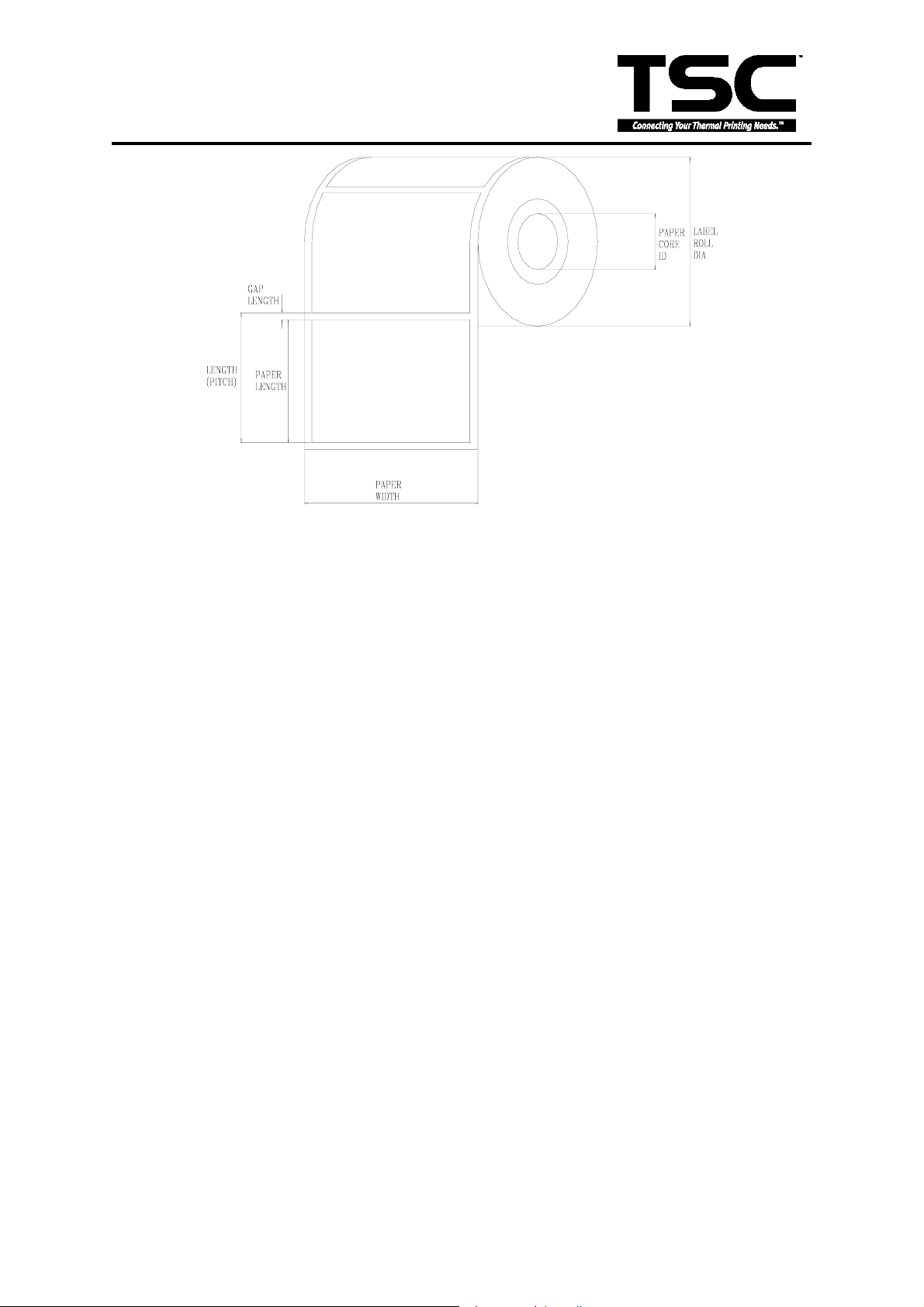
2.2 Specifications
Items Label
Paper Width
Length (Pitch)
Paper
Thickness
Paper Weight Max 240 g/m2
Max. Roll
Diameter
(1” core)
Roll Up Method Print surface wound outside as standard
Paper Core ID.
Note: (1). The width and thickness quoted above are said of the label plus its backing
paper.
(2). Likewise, the approval of label entails that of its backing paper.
(3). In the peel off mode, the minimum pitch is 35mm.
(4). In the cutter mode, it is required the paper be wound outside. Otherwise,
paper jam tends to result.
(5). In the cutter mode, the paper thickness is 0.2 mm at maximum, and the paper
weight is 100 g/m
(6). Paper shape is as shown on next page.
(7) Tag is 0.2mm in thickness, and is less than 100g/m
Max.114mm
Min. 25mm
12∼2286mm
0.20 mm
Inner roll diameter. Max 4.3” (110mm)
External roll diameter. Max 8.4”
(214mm)
φ25.7±0.3mm
2
at maximum.
2
in weight.
9
TTP-243 Bar Code Printer
Service Manua
l
10
TTP-243 Bar Code Printer
Service Manua
l
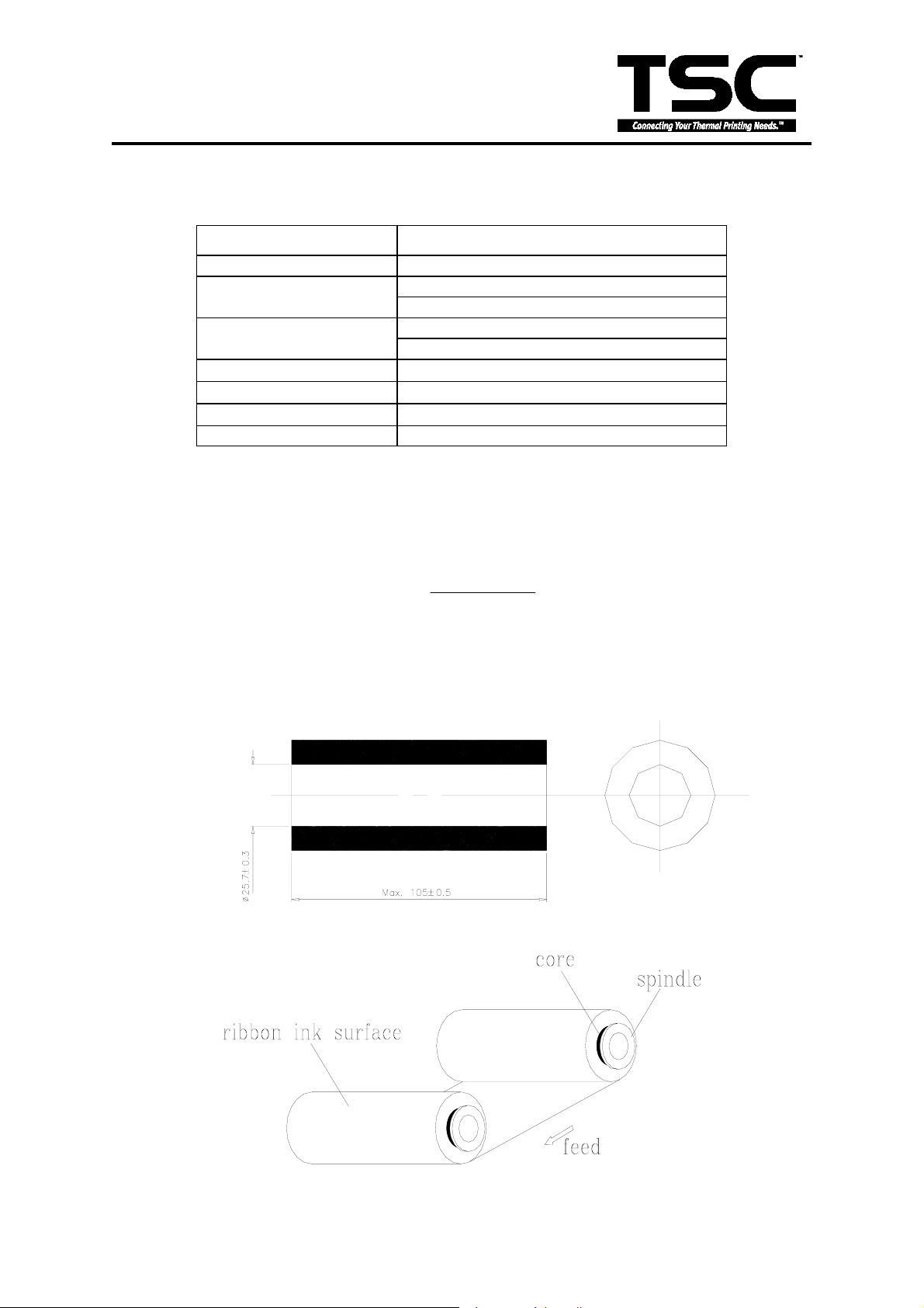
2.3 Ribbon Sizes and Shapes
Item Specifications
Ribbon shape Spool type
Ribbon width
Ribbon winding width
Leading tape
End tape
Max. ribbon OD.
Winding method Ink surface to be wound outside
Max. 110mm
Min. 40mm
Max. 110mm
Min. 40mm
Polyester film, 335±5mm long
Polyester film (transparent), 250±5mm long
φ67mm
Note: The maximum length of ribbon depends on its thickness and core outside diameter.
The formula below defines the correlation between ribbon roll length and ribbon core
diameter.
22
π
)d(D
= L
L = Ribbon length
D = Max. roll diameter
d = Ribbon core outside diameter
t = Ribbon thickness
×−
t4
where
,
11
TTP-243 Bar Code Printer
M
Service Manua
l
3. ELECTRONICS
3.1 Circuit Description
R8
3.3KR91.8K
GAP_EMITTER
74LS05
R10
910
PH_DETECT SENSOR
POWER LED
ONLINE LED
ERROR LED
PAUSE BUTTON
FEED BUTTON
RIBBON SENSOR
PEEL SENSOR
B.L. SENSOR
GAP SENSOR
DECODER SENSOR
CUTTER SENSOR
BUZZER
56
U7C
8 9
74LS05
R11
430
COMMUNICATION SYSTEM
U7A
74LS05
34
U7B
74LS05
U7D
/ERROR
/ERROR
SELECT
SELECT
12
DO0
DO1
DO2
DO3
DO4
DO5
DO6
55
VCC
VCC88AVCC89VREF
P106/MA8
P107/MA9
P105/RAS
P104/CAS
P56/TB0IN
P55/TA4IN
P52/TA3OUT
P50/TA2OUT
P51/TA2IN
P54/TA4OUT
P61/RTP01
P91/DMAREQ0
P87/TXD1
P85/CLK1
90
A0/MA0
A1/MA1
A2/MA2
A3/MA3
A4/MA4
A5/MA5
A6/MA6
A7/MA7
A8/D8
A9/D9
A10/D10
A11/D11
A12/D12
A13/D13
A14/D14
A15/D15
P44/QCL
P43/MX
P70/AN0
P71/AN1
P76/AN6
P77/AN7
P75/AN5
C70
0.1u
C49
0.1u
DO7
P92
R/W
ST0
ST1
76
83
RESET
36
RESETOUT
VSS
35
40
24
P84/CTS1/RTS1
M37721S1AFP
CNVSS
AVSS91VSS
34
92
P101/INT123P100/INT0
P93/DMAREQ1
U1
RDY31HOLD32BYTE
33
41
97
P73/AN3
85
蜂鳴器
2
C2
0.1u
16MHz
P82/RXD0
87
P80/CTS0/RTS0
84
P83/TXD0
86
P81/CLK0
2
P66/RTP12
1
P67/RTP13
79
P90/DMAACK0
22
P102/INT2
96
P74/AN4
27
P45/VDA
26
P46/VPA
25
P47/DBC
98
P72/AN2
8
P60/RTP00
6
P62/RTP02
3
P65/RTP11
5
P63/RTP03
4
P64/RTP10
9
P57/TB1IN
13
P53/TA3IN
81
P86/RXD1
21
P103/TC
30
46
BHE
72
P97/DMAREQ3
73
P96/DMAACK3
74
P95/DMAREQ2
75
P94/DMAACK2
45
BLE
37
XIN
X1
R13
1M
38
XOUT
U2
OUT1VCC
GND
S-807
3
RX2
RX2
RX1
RX1
TX1
TX1
TX2
TX2
PE
PE
INT
INT
C3
20P
C4
20P
+5V
DO[0..7]
ALE
44
ALE
A23/D748A22/D649A21/D550A20/D451A19/D352A18/D253A17/D154A16/D0
77
MA0
71
MA1
70
69
MA2
68
MA3
67
MA4
66
MA5
65
MA6
64
MA7
18
MA8
17
MA9
63
A8
62
A9
61
A10
60
A11
59
A12
58
A13
57
A14
56
A15
19
/RAS
20
/CAS
39
/E
E
R/W
47
43
ST0
42
ST1
10
11
14
16
15
12
7
78
80
28
29
100
82
99
94
93
RDY
95
+5V
L5
L21
L1
MA[0..9]
ST0
ST1
U5E
74HC04
1011
MA[0..9]
A[8..15]
4
5
1
2
74HC32
U24B
U24A
74HC32
MOTOR SYSTEM
PHASE1
PHASE1
PHASE2
PHASE2
I1
I1
I0
I0
PHASE3
PHASE3
DCM
DCM
CUTTER
CUTTER
MOTOR
MOTOR
R/W
R/W
PRINT SYSTEM
DI
DI
/LAT
/LAT
HISTORY
HISTORY
Vdet
Vdet
CLK
CLK
TM
TM
PH_HEAT
PH_HEAT
PH
PH
6
U24C
9
10
3
74HC32
8
MEMORY SYSTE
/RAS
/RAS
DRAMWR
DRAMWR
DRAMOE
DRAMOE
/OE
/OE
R/W
R/W
C1
C7
10u
0.1u
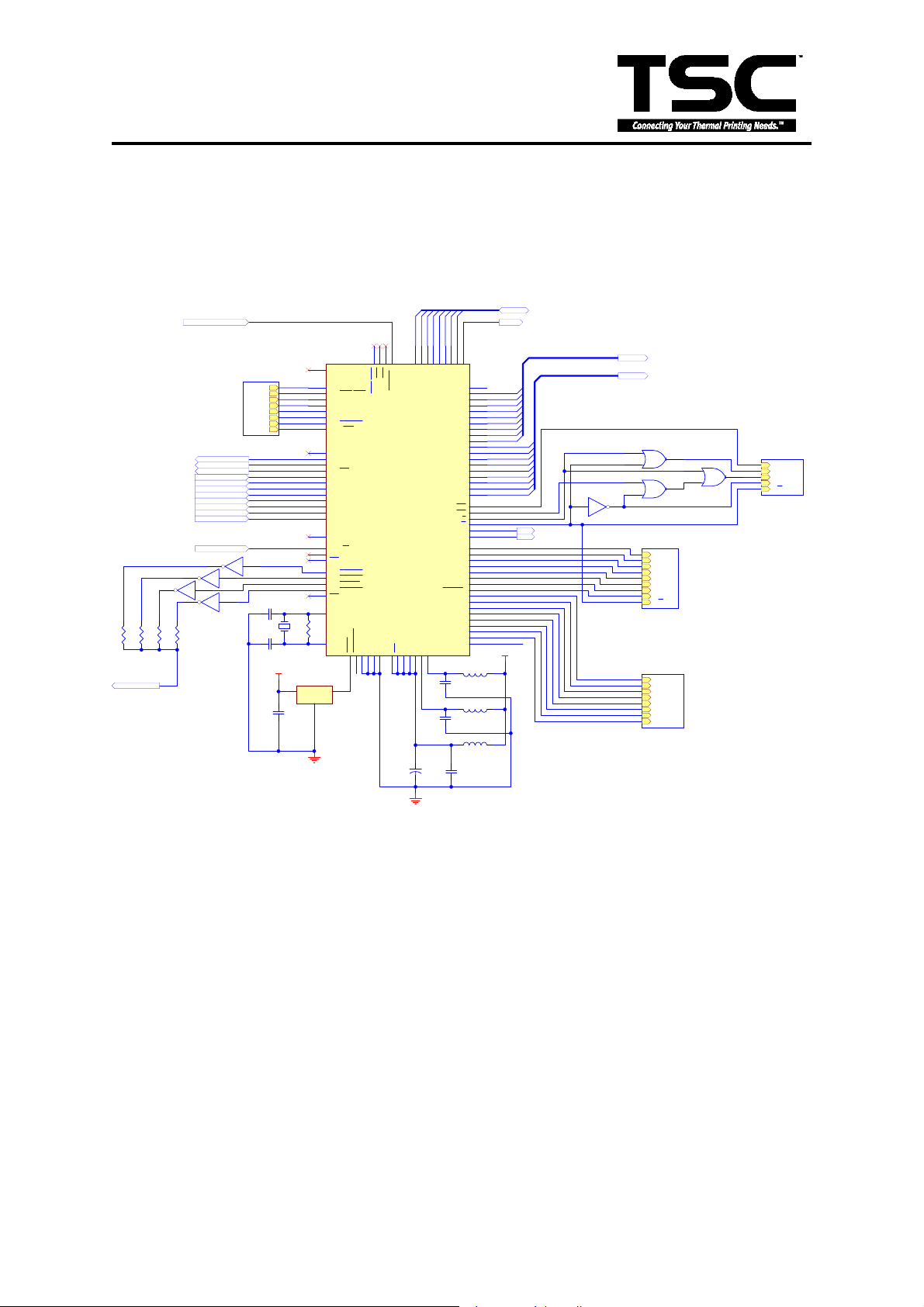
Fig. 3.1 MCU Circuit Diagram
The above is the MCU circuit diagram.
The main board of TTP-243 includes five system blocks:
A. Memory System (decoder & memory block)
B. Motor System (stepping motor, DC motor and cutter block)
C. Print head System
D. Communication System (serial & parallel port block)
E. Power System
The figure below shows the PCB system area.
12
TTP-243 Bar Code Printer
Motor System
Service Manua
l
Real Time Clock
Communication Port
Memory
Decoder System
Print Head
Cutter System
Memory System
13
External Memory
Connector
Power System
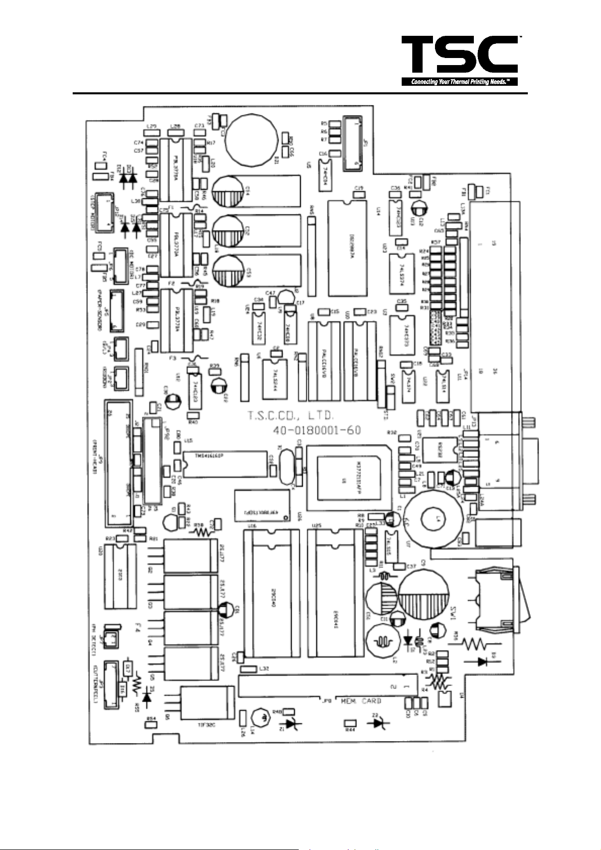
TTP-243 Bar Code Printer
g
Service Manua
l
. 3.2 System Block of PCB
Fi
14

TTP-243 Bar Code Printer
Service Manua
l
3.2 MCU Pin Description
Pin Name Input/Output Function
Vcc, Vss Power supply
CNVss CNVss input Input This pin controls the processor mode.
/RESET Reset input Input To enter the reset state, this pin must be
XIN Clock input Input
X
Clock output Output
OUT
/E Enable output Output Data/instruction read and data write are
BYTE Bus width
Input In memory expansion mode or
selection input
/HOLD /HOLD input
Input This is an input pin for the /HOLD
pin
/RDY /RDY input pin
ψ1 Clock ψ1
Input
Output
output
ST0, ST1 Status signal
Output The bus use status output is generated
output pin
Supply 5V±10% to Vcc and 0V to Vss.
Connect to Vss for single-chip mode,
and to Vcc for external ROM types.
kept at “L” condition, and maintained for
the required time.
These are I/O pins of internal clock
generating circuit. Connect a ceramic or
quartz crystal resonator between X
X
. When an external clock is used,
OUT
IN
and
the clock source should be connected to
the X
pin, and the X
IN
pin and should
OUT
be left open.
performed when output from this pin is
“L”.
microprocessor mode, this pin
determines whether the external data
bus is 8-bit width or 16-bit width. The
width is 16 bits for “L” signal input and 8
bits for “H” signal input.
request signal.
This is an input pin for the /RDY signal.
This is theψ1 output pin which is
divided the clock X
pin by 2.
IN
in 2-bit code
AVcc, AVss Analog supply
input
V
Reference
REF
voltage input
A0/MA0~
A7/MA7
Address
low-order/DRA
M address
Power supply for the A-D converter.
Connect AV
and AVSS to VSS
CC
externally.
Input This is reference voltage input pin for
the A-D converter.
Output This is an output pin for the 8 low-order
bits of addresses. When the DRAM is to
be accessed, the row and column
addresses are generated by means of
time division multiplexing.
15

TTP-243 Bar Code Printer
Service Manua
l
A8/D8~
A15/D15
Address
medium-order/
data high-order
A16/D0~
A23/D7
Address high-
order/data
low-order
R/W, /BHE
ALE, /BHE
P40~P4
P50~P5
P60~P6
P70~P7
P80~P8
P90~P9
Memory Control
signal output
I/O port P4 I/O
7
I/O port P5 I/O
7
I/O port P6 I/O
7
I/O port P7 I/O
7
I/O port P8 I/O
7
I/O port P9 I/O
7
P100~P107 I/O port P10 I/O
I/O When the BYTE pin is set to “L” in memory
expansion mode or microprocessor mode and
external data bus is 16-bit width, high-order
data (D15~D8) is input or output when /E
output is “L” and an address (A15~A8) is
output when /E output is “H”.
If the BYTE pin is “H” that is an external data
bus is 8-bit width, only address (A15~A8) is
output.
I/O
In memory expansion mode or microprocessor
mode low-order data (D7~D0) is input or output
when /E output is “L” and an address (A23~A16) is
output when /E output is “H”.
Output These are R/W, /BHE, ALE, and /BLE output
pins.
This port is provided 5-bit I/O. As it has an I/O
register, it is possible to perform programming to
determine whether each bit serves as an input pin
or an output pin.
This port is used for 8-bit I/O. It has basically the
same function as port P4. In addition, it provides
the timer A2, timer A3, timer A4 I/O pins and
TimeB0 and TimeB1 input pins.
This port is used for 8-bit I/O. It has basically the
same function as port P4. In addition, pins P60
through P63 and pins P64 through P67 are
capable of functioning as a 4-bit real-time output,
respectively.
This port is used for 8-bit I/O. It has basically the
same function as port P4. In addition, it provides
the input pins for analog inputs AN0 through AN7.
Pin P77 is also used for A-D conversion start
trigger input.
This port is used for 8-bit I/O. It has basically the
same function as port P4. In addition, it provides
RxD, TxD, CLK, /CTS//RTS terminals for UART 0
and UART 1.
This is an 8-bit I/O port. It has basically the same
function as port P4. In addition, it provides the
DMA request input pin and DMA acknowledge
signal output pin.
This is an 8-bit I/O port. It has basically the same
function as port P4. In addition, it provides the
/INT0, /INT1, /INT2 input pins, /TC I/O pins, and
/RAS, /CAS, MA8, MA9 output pin.
16

TTP-243 Bar Code Printer
Service Manua
l
3.3 Reset Circuit
VCC
U2
2
C2
0.1u
VCC
OUT
GND
3
1
/RESET
CONNECT WITH MCU RESET PIN
S-807
Fig. 3.3 Reset Circuit
This is the reset circuit .The 80746ALO IC outputs the system reset signal of “LOW”
when the driving voltage is lower than 4.6V (Typical).
3.4 Memory System
A[0..18]
MA[0..9]
DO[0..7]
A[8..18]
MA[0..9]
/LCAS
/UCAS
DRAMWR
DRAMOE
R/W
ROM1
ROM2
DO[0..7]
VCC
1
6
21
MA0
17
A0
MA1
18
A1
19
MA2
A2
20
MA3
A3
23
MA4
A4
24
MA5
A5
25
MA6
A6
26
MA7
A7
27
MA8
A8
28
MA9
A9
16
NC/A10
15
NC/A11
TMS416160P
14
/RAS
/OE
RAS
31
LCAS
30
UCAS
13
W
29
OE
2
DO0
DQ0
VCC
VCC
VCC
3
DO1
DQ1
4
DO2
DQ2
5
DO3
DQ3
7
DO4
DQ4
8
DO5
DQ5
9
DO6
DQ6
10
DO7 A8
DQ7
DO0
33
DQ8
34
DO1
DQ9
U15
35
DO2
DQ10
36
DO3
DQ11
38
DO4
DQ12
39
DO5
DQ13
40
DO6
DQ14
41
DO7
DQ15
11
NC
12
NC
32
NC
GND
GND
GND
22
37
42
U16
MA0
11
MA1
10
MA2
9
MA3
8
MA4
7
MA5
6
MA6
5
MA7
27
26
A9
23
A10
25
A11
4
A12
28
A13
29
A14
3
A15
2
A16
30
A17
1
A18
29C040
A012AD0
A1
A2
A3
A4
A5
A6
A7
A8
A9
A10
A11
A12
A13
A14
A15
A16
A17
A18
13
DO0
14
DO1
AD1
15
DO2
AD2
17
DO3
AD3
18
DO4
AD4
19
DO5
AD5
20
DO6
AD6
21
DO7
AD7
16
GND
32
VCC
VCC
31
WE
24
OE
22
CE
U25
MA0
A012AD0
11
MA1
A1
10
MA2
A2
9
MA3
A3
8
MA4
A4
7
MA5
A5
6
MA6
A6
5
MA7
A7
A8
27
A8
A9
26
A9
A10
23
A10
25
A11
A11
4
A12
A12
28
A13
A13
29
A14
A14
3
A15
A15
2
A16
A16
30
A17
A17
1
A18
A18
29C040
Fig. 3.4 FLASH ROMS and DRAM Diagram
This is the memory circuit. The U16&U17 type 512K Byte FLASH ROM and U15 type
2M Byte DRAM are used. The MCU R/W pin becomes “H” when reading Flash ROM or
DRAM, and “L” when writing.
DO0
13
14
DO1
AD1
15
DO2
AD2
17
DO3
AD3
18
DO4
AD4
19
DO5
AD5
20
DO6
AD6
21
DO7
AD7
16
GND
32
VCC
VCC
31
WE
24
OE
22
CE
17
TTP-243 Bar Code Printer
C
Service Manua
l
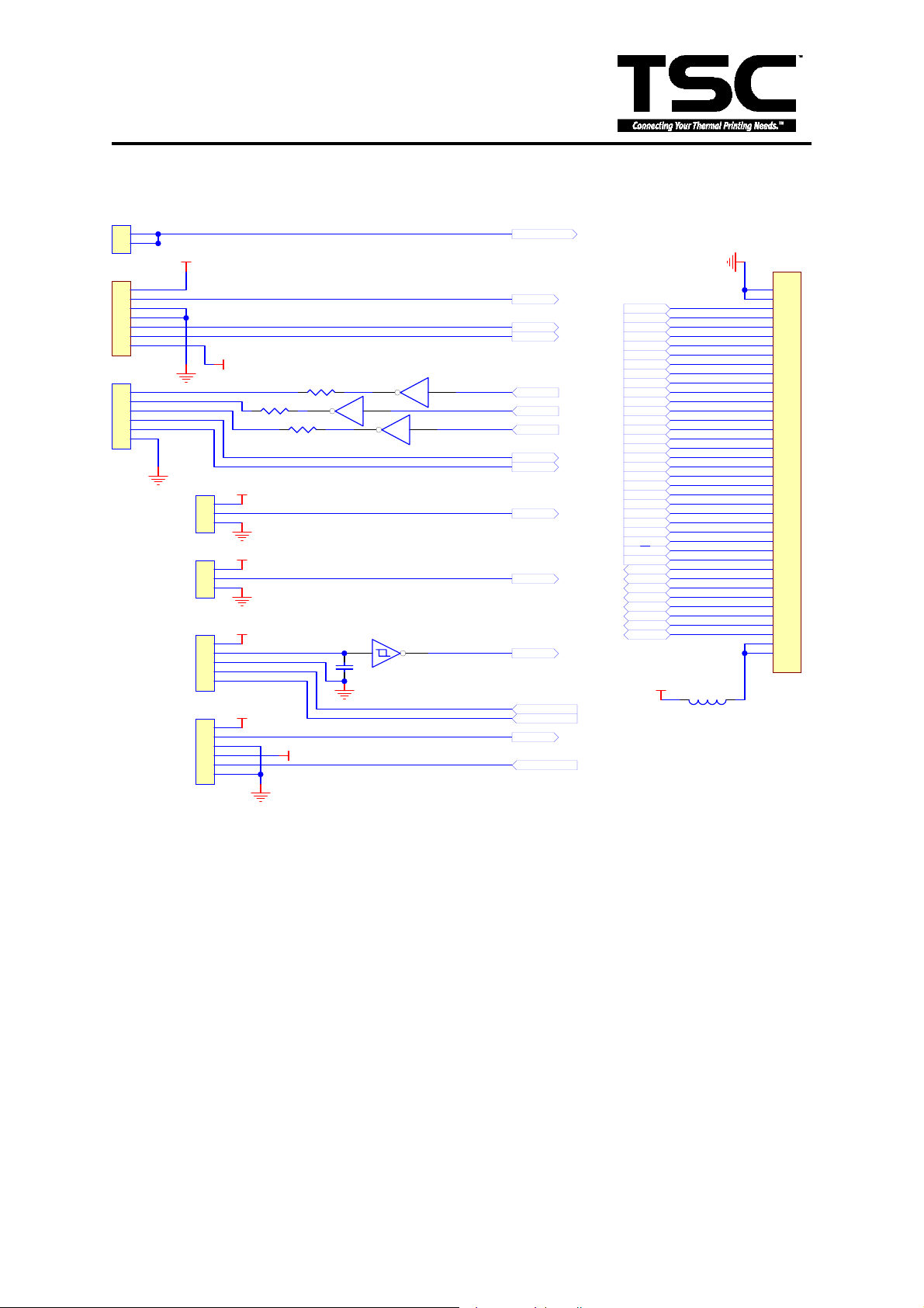
3.5 Connector Circuit Diagram
1
1
2
2
PH_DERECT
PH_DERECT
JP3
7
6
5
4
3
2
1
ER&PEEL
JP1
1
2
3
4
5
6
6 PIN
JP8
+5V
+24V
U5A
74HC04
12
56
JP2
RIBBON
JP4
B.L.
JP6
DC MOTOR
JP5
6 PIN
R5
100
R6
100
74HC04
R7
100
+5V
1
2
3
+5V
1
2
3
+5V
1
2
3
DCMA
4
5
DCMB
+5V
1
2
3
4
5
6
+5V
34
U5B
74HC04
U11A
1 2
C68
74LS14
0.1u
U5C
Fig. 3.5 Connector Circuit Diagram
PH_DETECT
P65
CUTTER
P53
P45
P46
P47
P72
P60
P62
P63
P57
DC_MOTOR_A
DC_MOTOR_B
P64
GAP_EMITTER
1
2
MA0
MA1
MA2
MA3
MA4
MA5
MA6
MA7
A8
A9
A10
A11
A12
A13
A14
A15
A16
A17
A18
A19
A20
A21
A22
A23
/RESET
/E
R/W
OE
DO0
DO1
DO2
DO3
DO4
DO5
DO6
DO7
+5V
L32
BEAD
3
4
5
6
7
8
9
10
11
12
13
14
15
16
17
18
19
20
21
22
23
24
25
26
27
28
29
30
31
32
33
34
35
36
37
38
39
40
Memory card connector
JP8
MEM.
P45~P47 are output pins from MCU, which control the Power-on, Feed and Error LEDs
respectively. The LED lights on when the signal is “low”, goes out when the signal is
“on”.
P72: the detect pin of push button.(normally at ‘high’ level)
P60: the detect pin of feed button. (normally at ‘high’ level)
P65: the detect pin of the peel-off sensor. (normally at ‘high’ level)
P62: the detect pin of the ribbon sensor. (normally at ‘high’ level)
P63: the detect pin of the black mark sensor. (normally at ‘high’ level)
P64: the detect pin of the gap sensor and print head micro sensor. (normally at ‘high’
level)
18
 Loading...