

Page 1
Surface Mount Transient Voltage Suppressor
P6SMB SERIES
Voltage Range
6.8 to 200 Volts
600 Watts Peak Power
Features
a For surface mounted application in order to optimize board
space
a Low profile package
a Built-in strain relief
a Glass passivated junction
a Excellent clamping capability
a Fast response time: Typically less than 1.0ps from 0 volt to
BV min.
a Typical I
a High temperature soldering guaranteed:
a Plastic material used carries Underwriters Laboratory
a 600 watts peak pulse power capability with a 10 x 1000 us
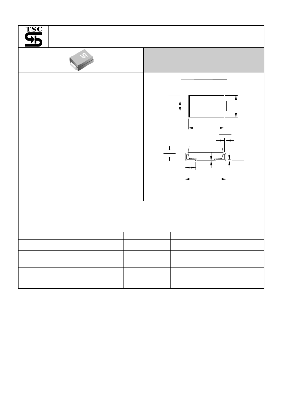
Mechanical Data
a Case: Molded plastic
a Terminals: Solder plated
a Polarity: Indicated by cathode band
a Standard packaging: 12mm tape (EIA STD RS-481)
a
less than 1A above 10V
R
O
C / 10 seconds at terminals
250
Flammability Classification 94V-0
waveform by 0.01% duty cycle
Weight: 0.093gram
.103(2.61)
.078(1.99)
Dimensions in inches and (millimeters)
SMB/DO-214AA
.082(2.08)
.076(1.93)
.056(1.41)
.035(0.90)
.187(4.75)
.167(4.25)
.208(5.28)
.200(5.08)
.008(.20)
.004(.10)
.012(.31)
.006(.15)
.147(3.73)
.137(3.48)
.012(.31)
.006(.15)
Maximum Ratings and Electrical Characteristics
Rating at 25ambient temperature unless otherwise specified.
ote 1)
=25OC,
T
A
2
(.013 mm Thick) Copper Pads to Each Terminal.
Symbol Value Units
PPK Minimum 600 Watts
I
FSM
V
TJ, T
F
-65 to + 150
STG
100
3.5
Amps
Volts
Type Number
eak Power Dissipation at
P
Tp=1ms(
Peak Forward Surge Current, 8.3 ms Single Half
Sine-wave Superimposed on Rated Load
(JEDEC method) (Note 2, 3) - Unidirectional Only
Maximum Instantaneous Forward Voltage at
50.0A for Unidirectional Only (Note 4)
Operating and Storage Temperature Range
Notes: 1. Non-repetitive Current Pulse Per Fig. 3 and Derated above TA=25OC Per Fig. 2.
2. Mounted on 5.0mm
Devices for Bipolar Applications
2. Electrical Characteristics Apply in Both Directions.
N
3. 8.3ms Single Half Sine-wave or Equivalent Square Wave, Duty Cycle=4 pulses Per Minute
Maximum.
1. For Bidrectional Use C or CA Suffix for Types P6SMB6.8 through Types P6SMB200A.
O
C
- 110 -
Page 2

ELECTRICAL CHARACTERISTICS (TA=25OC unless otherwise noted)
Device Device
Marking
Code
P6SMB6.8 KDJ 6.12 7.48 10 5.50 1000 58 10.8 0.057
P6SMB6.8A KEJ 6.45 7.14 10 5.80 1000 60 10.5 0.057
P6SMB7.5 KFJ 6.75 8.25 10 6.05 500 53 11.7 0.061
P6SMB7.5A KGJ 7.13 7.88 10 6.40 500 55 11.3 0.061
P6SMB8.2 KHJ 7.38 9.02 1.0 6.63 200 50 12.5 0.065
P6SMB8.2A KKJ 7.79 8.61 1.0 7.02 200 52 12.1 0.065
P6SMB9.1 KLJ 8.19 10.0 1.0 7.37 50 45 13.8 0.068
P6SMB9.1A KMJ 8.65 9.55 1.0 7.78 50 47 13.4 0.068
P6SMB10 KNJ 9.00 11.0 1.0 8.10 10 42 15.0 0.073
P6SMB10A KPJ 9.50 10.5 1.0 8.55 10 43 14.5 0.073
P6SMB11 KQJ 9.90 12.1 1.0 8.92 5.0 38 16.2 0.075
P6SMB11A KRJ 10.5 11.6 1.0 9.40 5.0 40 15.6 0.075
P6SMB12 KSJ 10.8 13.2 1.0 9.72 5.0 36 17.3 0.078
P6SMB12A KTJ 11.4 12.6 1.0 10.2 5.0 37 16.7 0.078
P6SMB13 KUJ 11.7 14.3 1.0 10.5 5.0 33 19.0 0.081
P6SMB13A KVJ 12.4 13.7 1.0 11.1 5.0 34 18.2 0.081
P6SMB15 KWJ 13.5 16.5 1.0 12.1 5.0 28 22.0 0.084
P6SMB15A KXJ 14.3 15.8 1.0 12.8 5.0 29 21.2 0.084
P6SMB16 KYJ 14.4 17.6 1.0 12.9 5.0 26 23.5 0.086
P6SMB16A KZJ 15.2 16.8 1.0 13.6 5.0 28 22.5 0.086
P6SMB18 LDJ 16.2 19.8 1.0 14.5 5.0 23 26.5 0.088
P6SMB18A LEJ 17.1 18.9 1.0 15.3 5.0 25 25.2 0.088
P6SMB20 LFJ 18.0 22.0 1.0 16.2 5.0 21 29.1 0.090
P6SMB20A LGJ 19.0 21.0 1.0 17.1 5.0 22 27.7 0.090
P6SMB22 LHJ 19.8 24.2 1.0 17.8 5.0 19 31.9 0.092
P6SMB22A LKJ 20.9 23.1 1.0 18.8 5.0 20 30.6 0.092
P6SMB24 LLJ 21.6 26.4 1.0 19.4 5.0 18 34.7 0.094
P6SMB24A LMJ 2 2.8 25.2 1.0 20.5 5.0 19 33.2 0.094
P6SMB27 LNJ 24.3 29.7 1.0 21.8 5.0 16 39.1 0.096
P6SMB27A LPJ 25.7 28.4 1.0 23.1 5.0 16.8 37.5 0.096
P6SMB30 LQJ 27.0 33.0 1.0 24.3 5.0 14 43.5 0.097
P6SMB30A LRJ 28.5 31.5 1.0 25.6 5.0 15 41.4 0.097
P6SMB33 LSJ 29.7 36.3 1.0 26.8 5.0 13.0 47.7 0.098
P6SMB33A LTJ 31.4 34.7 1.0 28.2 5.0 13.8 45.7 0.098
P6SMB36 LUJ 32.4 39.6 1.0 29.1 5.0 12 52.0 0.099
P6SMB36A LVJ 34.2 37.8 1.0 30.8 5.0 12.6 49.9 0.099
P6SMB39 LWJ 35.1 42.9 1.0 31.6 5.0 11.1 56.4 0.100
P6SMB39A LXJ 37.1 41.0 1.0 33.3 5.0 11.6 53.9 0.100
P6SMB43 LYJ 38.7 47.3 1.0 34.8 5.0 10.0 61.9 0.101
P6SMB43A LZJ 40.9 45.2 1.0 36.8 5.0 10.6 59.3 0.101
P6SMB47 MDJ 42.3 51.7 1.0 38.1 5.0 9.2 67.8 0.101
P6SMB47A MEJ 44.7 49.4 1.0 40.2 5.0 9.7 64.8 0.101
P6SMB51 MFJ 45.9 56.1 1.0 41.3 5.0 8.5 73.5 0.102
P6SMB51A MGJ 48.5 53.6 1.0 43.6 5.0 8.9 70.1 0.102
P6SMB56 MHJ 50.4 61.6 1.0 45.4 5.0 7.8 80.5 0.103
P6SMB56A MKJ 53.2 58.8 1.0 47.8 5.0 8.1 77.0 0.103
P6SMB62 MLJ 55.8 68.2 1.0 50.2 5.0 7.0 89.0 0.104
P6SMB62A MMJ 58.9 65.1 1.0 53.0 5.0 7.4 85.0 0.104
P6SMB68 MNJ 61.2 74.8 1.0 55.1 5.0 6.4 98.0 0.104
P6SMB68A MPJ 64.6 71.4 1.0 58.1 5.0 6.8 92.0 0.104
P6SMB75 MQJ 67.5 82.5 1.0 60.7 5.0 5.8 108.0 0.105
P6SMB75A MRJ 71.3 78.8 1.0 64.1 5.0 6.1 103.0 0.105
P6SMB82 MSJ 73.8 90.2 1.0 66.4 5.0 5.3 118.0 0.105
P6SMB82A MTJ 77.9 86.1 1.0 70.1 5.0 5.5 113.0 0.105
BR
V
(Volts) (Note 1)
Min Max (mA) (Volts) ID (uA) (Note 2)(Amps) VC(Volts) of VBR(% / OC)
Breakdown Voltage
Test Stand-Off Maximum Maximum Maximum Maximum
Current Voltage Reverse Leakage Peak Pulse Clamping Temperature
T
@I
WM
V
at V
WM
Current I
RSM
Voltage at I
PPM
Coefficient
- 111 -
Page 3

ELECTRICAL CHARACTERISTICS (TA=25OC unless otherwise noted)
Device Device
Marking
P6SMB91 MUJ 81.9 100.0 1.0 73.7 5.0 4.8 131.0 0.106
P6SMB91A MVJ 86.5 95.5 1.0 77.8 5.0 5.0 125.0 0.106
P6SMB100 MWJ 90.0 110.0 1.0 81.0 5.0 4.3 144.0 0.106
P6SMB100A MXJ 95.0 105.0 1.0 85.5 5.0 4.5 137.0 0.106
P6SMB110 MYJ 99.0 121.0 1.0 89.2 5.0 3.9 158.0 0.107
P6SMB110A MZJ 105.0 116.0 1.0 94.0 5.0 4.1 152.0 0.107
P6SMB120 NDJ 108.0 132.0 1.0 97.2 5.0 3.6 173.0 0.107
P6SMB120A NEJ 114.0 126.0 1.0 102.0 5.0 3.8 165.0 0.107
P6SMB130 NFJ 117.0 143.0 1.0 105.0 5.0 3.3 187.0 0.107
P6SMB130A NGJ 124.0 137.0 1.0 111.0 5.0 3.5 179.0 0.107
P6SMB150 NHJ 135.0 165.0 1.0 121.0 5.0 2.9 215.0 0.108
P6SMB150A NKJ 143.0 158.0 1.0 128.0 5.0 3.0 207.0 0.108
P6SMB160 NLJ 144.0 176.0 1.0 130.0 5.0 2.7 230.0 0.108
P6SMB160A NMJ 152.0 168.0 1.0 136.0 5.0 2.8 219.0 0.108
P6SMB170 NNJ 153.0 187.0 1.0 138.0 5.0 2.5 244.0 0.108
P6SMB170A NPJ 162.0 179.0 1.0 145.0 5.0 2.6 234.0 0.108
P6SMB180 NQJ 162.0 198.0 1.0 146.0 5.0 2.4 258.0 0.108
P6SMB180A NRJ 171.0 189.0 1.0 154.0 5.0 2.5 246.0 0.108
P6SMB200 NSJ 180.0 220.0 1.0 162.0 5.0 2.1 287.0 0.108
P6SMB200A NTJ 190.0 210.0 1.0 171.0 5.0 2.2 274.0 0.108
Notes:
BR measured after IT applied for 300us, IT=square wave pulse or equivalent.
1. V
2. Surge current waverform per Figure 3 and derate per Figure 2.
3. For bipolar types having V
4. For bidirectional use C or Ca suffix for types P6SMB6.8 through P6SMB200A.
5. All terms and symbols are consistent with ANSI/IEEE C62.35.
Breakdown Volta Test Stand-Off Maximum Maximum Maximum Maximum
V
(Volts) (Note 1 @I
Code
BR
Current Voltage Reverse Leakage Peak Pulse Clamping Temperature
T
WM
V
at V
WM
Current I
RSM
Voltage at I
Min Max (mA) (Volts) ID (uA) (Note 2)(Amps) VC(Volts) of VBR(% / OC)
of 10 volts and under, the ID limit is doubled.
WM
PPM
Coefficient
- 112 -
Page 4
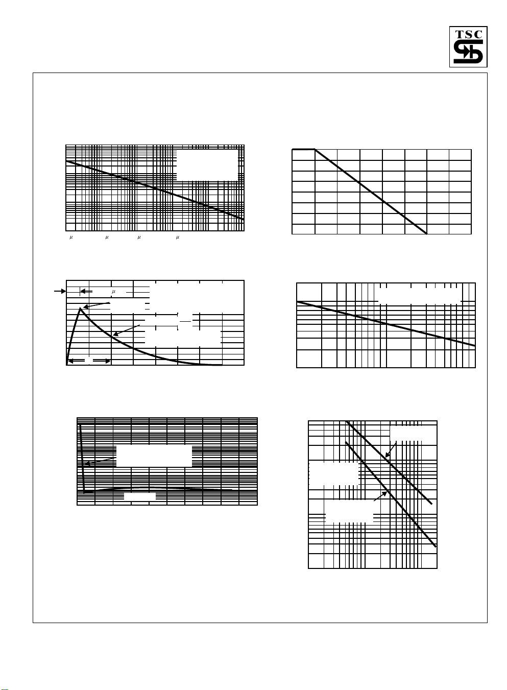
RATINGS AND CHARACTERISTIC CURVES (P6SMB SERIES)
FIG.1- PEAK PULSE POWER RATING CURVE
100
10
1.0
PPM
0.1
P , PEAK PULSE POWER, KW
0.1 s 1.0 s 10 s 100 s 1.0ms 10ms
tp, PULSE WIDTH, sec.
NON-REPETITIVE
PULSE WAVEFORM
SHOWN in FIG.3
O
T=25C
A
FIG.3- PULSE WAVEFORM
150
tr = 10 sec
Peak Value
PPM
100
50
PEAK PULSE CURRENT - %
0
0 1.0 2.0 3.0 4.0
I
td
PULSE WIDTH (td) is DEFINED
as the POINT WHERE the PEAK
CURRENT DECAYS
PPM
to 50% of I
I
Half Value -
10/1000 sec. WAVEFORM
as DEFINED by R.E.A.
PPM
2
t, TIME, ms
FIG.5- TYPICAL REVERSE LEAKAGE CHARACTERASTICS
1,000
100
10
1
0.1
0.01
CURRENT, MICROAMPERES
0.001
0 100 200 300 400 500
D
I , INSTANTANEOUS REVERSE LEAKAGE
MEASURED AT DEVICES
STAND-OFF
VOLTAGE, V
O
TA=25 C
WM
V , BREAKDOWN VOLTAGE. VOLTS(BR)
FIG.2- PULSE DERATING CURVE
100
75
PP
50
25
DERATING IN PERCENTAGE. %
0
0 25 50 75 100 125 150 175 200
PEAK PULSE POWER (P ) or CURRENT (IPPM)
FIG.4- MAXIMUM NON-REPETITIVE FORWARD SURGE
200
100
TA, AMBIENT TEMPERATURE. ( C)
CURRENT UNIDIRECTIONAL ONLY
8.3ms Single Half Sine Wave
JEDEC Method
AMPERES
10
1 10 100
IFSM, PEAK FORWARD SURGE CURRENT.
FIG.6- TYPICAL JUNCTION CAPACITANCE
6,000
1,000
100
NUMBER OF CYCLES AT 60Hz
UNIDIRECTIONAL
O
Tj =25 C
f = 1.0MHz
Vsig=50mVp-p
MEASURED at
STAND-OFF
VOLTAGE, V
WM
O
MEASURED at
ZERO BIAS
-113-
J
C ,JUNCTION CAPACITANCE. (pF)
10
1.0 10 100 200
V , BREAKDOWN VOLTAGE. VOLTS(BR)
Page 5

 Loading...