

TriQuint Semiconductor Inc TQ9222 Datasheet
WIRELESS COMMUNICATIONS DIVISION
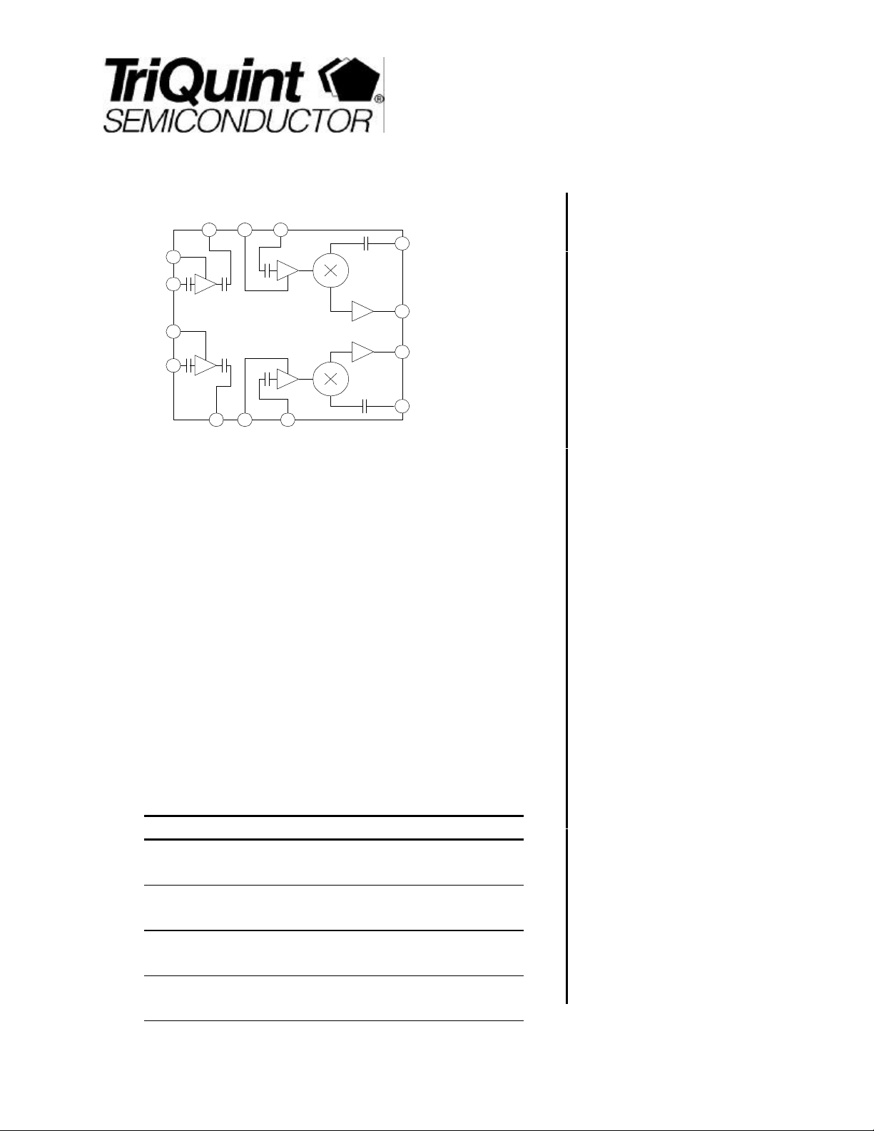
TQ9222
800
Vdd
MXR 1900
Vdd
MXR 800
MXR LO
1900
MXR LO
800
MXR RF
1900
MXR IF
1900
MXR IF
800
MXR RF
800
Vdd LNA
1900
LNA IN
1900
Vdd LNA
800
LNA IN
800
LNA OUT
1900
LNA OUT
Product Description
The TQ9222 is a 3-V, RF receiver IC designed specifically for dual-band TDMA
applications. Its RF performance meets the requirements of products designed to
the IS-136 and GSM standards. The TQ9222 is pin compatible with TQ5121 (cellular
band LNA/Mixer) which enables handset designers to use strategic board platform
strategy.
The TQ9222 contains two separate LNA+Mixer circuits to handle both the 800 MHz
cellular band and the 1900 MHz PCS band. The mixers use a high-side LO
frequency, with the IF covering a range of 70-140 MHz. IF frequencies below 120
MHz are possible due to the ½-IF spurious signal rejection in the 1900 MHz
LNA+Mixer. The IF outputs are designed for use of a common IF frequency. Most
RF ports are internally matched to 50Ω, greatly simplifying the design and keeping
the number of external components to a minimum. Separate supply voltage
connections provide the required flexibility for dual-band operation. The TQ9222
achieves good RF performance with low current consumption, supporting long
standby times in portable applications. Coupled with the very small QSOP-24
package, the part is ideally suited for dual-band mobile phones.
DATA SHEET
Dual-Band TDMA
LNA/Downconverter IC
Features
§ Pin compatible with TQ5121
§ Single 3 V operation
§ Low-current operation
§ Low-frequency IF capability
§ Excellent ½ IF rejection
§ IF output combining
§ 50 Ω matched inputs (most ports)
§ QSOP-24 plastic package
Applications
Electrical Specifications
1
§ IS-136 dual-band Mobile Phones
§ Tri-Mode Phones
Parameter Typ Units
Gain 800 band
1900 band
Noise Figure 800 band
1900 band
Input 3rd Order Intercept 800 band
1900 band
DC supply Current 800 band
1900 band
Note 1: Test Conditions: Vdd=2.8V, Ta=25C, filter IL=2.5dB, RF1=881MHz, RF 2=1960MHz,
LO1=991MHz, LO2= 2070MHz, IF=110MHz, LO Input=-7dBm; unless otherwise specified
17.5
17.5
2.7
3.0
-9.0
-9.0
10.0
22.0
MHz
MHz
dB
dB
dBm
dBm
mA
mA
For additional information and latest specifications, see our website: www.triquint.com 1
§ GSM dual-band Mobile Phones
§ Wireless local loop
TQ9222
Data Sheet
Electrical Characteristics
Parameter Conditions Min. Typ/Nom Max. Units
RF Frequency Cellular band
PCS band
LO Frequency Cellular band
PCS band
IF Frequency Cellular band 85 140 MHz
LO input level -7 -4 0 dBm
Supply voltage 2.7 2.8 3.0 V
Gain Cellular band
PCS band
Gain Variation vs. Temp. -40 to 85C -2.0 +2.0 dB
Noise Figure Cellular band
PCS band
Input 3rd Order Intercept Cellular band
PCS band
Return Loss
Cellular and PCS band
Isolation
Cellular and PCS bands
IF Output Impedance
Cellular and PCS band
Supply Current Cellular band
Note 1: Test Conditions: Vdd=2.8V, Ta=25C, filter IL=2.5dB, RF1=881MHz, RF2=1960MHz, LO1=991MHz, LO2= 2070MHz, IF=110MHz, LO Input=-7dBm; unless
otherwise specified
LNA input – external match
LNA output
Mixer RF input
Mixer LO input
LO to LNA in
LO to IF; after IF match
RF to IF; after IF match
Vdd = 2.8V; “ON”
Vdd = 0V; “OFF”
PCS band
Absolute Maximum Ratings
869
1930
950
2010
16.0
16.0
-11.0
-11.0
10
10
10
10
40
17.5
17.5
2.7
3.0
-9.0
-9.0
40
40
500
<50
10
22
894
1990
1040
2140
3.5
3.5
13 mA
MHz
MHz
MHz
MHz
dB
dB
dB
dB
dBm
dBm
dB
dB
dB
dB
dB
dB
dB
Ohm
Ohm
mA
Parameter Value Units
DC Power Supply 5.0 V
Power Dissipation 500 mW
Operating Temperature -40 to 85 C
Storage Temperature -60 to 150 C
Signal level on inputs/outputs +20 dBm
Voltage to any non supply pin -.3 to +.3 V
2 For additional information and latest specifications, see our website: www.triquint.com
TQ9222
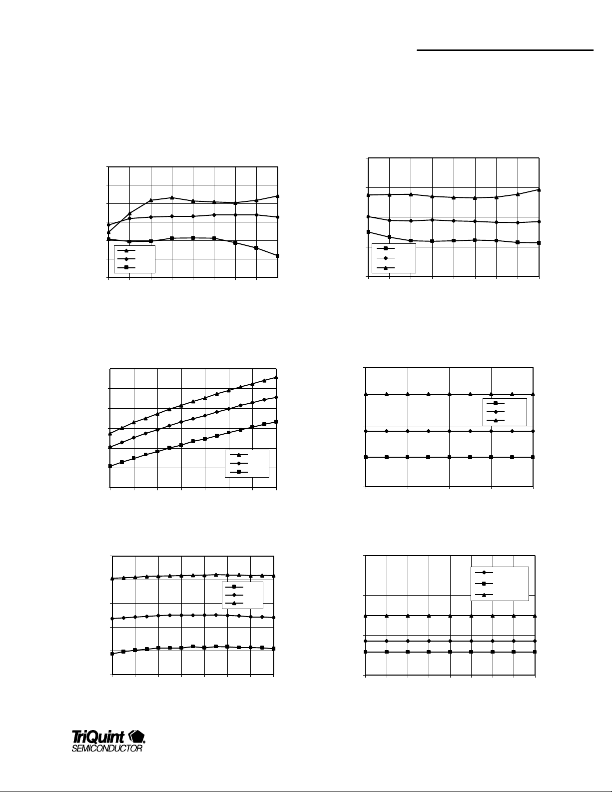
Conversion Gain vs. Vdd vs. Temp
Noise Figure vs. Freq vs. Temp
Data Sheet
Typical Performance
Test Conditions: TQ9222 Low Band (Unless Otherwise Specified): Vdd=2.8V, Ta=25C, filter IL=2.5dB, RF=881MHz, LO=991MHz, IF=110MHz, LO input=-7dBm
Conversion Gain vs. Freq vs. Temp
*Note: rolloff at -40C and +85C due to change in SAW filter Fc over temperature
20
5
19
18
17
Gain (dB)
16
15
14
869 872 875 878 881 884 887 890 893
20
19
18
17
Gain (dB)
16
15
14
2.5 2.6 2.7 2.8 2.9 3 3.1 3.2
-40C
+25C
+85C
Freq (MHz)
-40C
+25C
+85C
Vdd (volts)
4
3
Noise Figure (dB)
2
1
869 872 875 878 881 884 887 890 893
11
10
9
Idd (mA)
8
7
869 875 881 887 893
-40C
+25C
+85C
Freq (MHz)
Idd vs. Freq vs. Temp
-40 C
+25 C
+85 C
Freq (MHz)
-7
-8
-9
-10
IIP3 (dBm)
-11
-12
IIP3 vs. Vdd vs. Temp
-40C
+25C
+85C
2.5 2.6 2.7 2.8 2.9 3 3.1 3.2
Vdd (volts)
For additional information and latest specifications, see our website: www.triquint.com 3
Idd vs. Freq vs. Vdd
11
Vdd= 2.8v
Vdd= 2.7v
10
Idd (mA)
9
8
869 872 875 878 881 884 887 890 893
Freq (MHz)
Vdd= 3.0v

TQ9222
Data Sheet
Typical Performance:
Test Conditions: TQ9222 High Band (Unless Otherwise Specified): Vdd=2.8V, Ta=25C, filter IL=2.5dB, RF=1960MHz, LO=2070MHz, IF=110MHz, LO input=-7dBm
Conversion Gain vs. Freq. vs. Temp.
20
19
18
CG (dB)
17
16
15
1930 1940 1950 1960 1970 1980 1990
Conversion Gain vs. Vdd vs. TEMP
21
20
19
18
17
CG (dB)
16
15
14
2.5 2.6 2.7 2.8 2.9 3 3.1 3.2
Freq (MHz)
Vdd (v)
-40 C
+25 C
+85 C
-40 C
+25 C
+85 C
Noise Figure vs. Freq. vs. Temp.
5
4
3
NF (dB)
2
1
1930 1940 1950 1960 1970 1980 1990
Freq (MHz)
Idd vs Freq. vs Temp.
26
24
22
Idd (mA)
20
18
1930 1940 1950 1960 1970 1980 1990
Freq (MHz)
-40 C
+85 C
+25 C
-40 C
+25 C
+85 C
IIP3 vs. Vdd vs. TEMP
-7
-8
-9
-10
IIP3 (dBm)
-11
-12
-13
2.5 2.6 2.7 2.8 2.9 3 3.1 3.2
Vdd (v)
-40 C
+25 C
+85 C
26
24
22
Idd (mA)
20
18
1930 1940 1950 1960 1970 1980 1990
4 For additional information and latest specifications, see our website: www.triquint.com
Idd vs Freq. vs Vdd
Vdd= 2.7v
Vdd= 2.8v
Vdd= 3.0v
Freq (MHz)
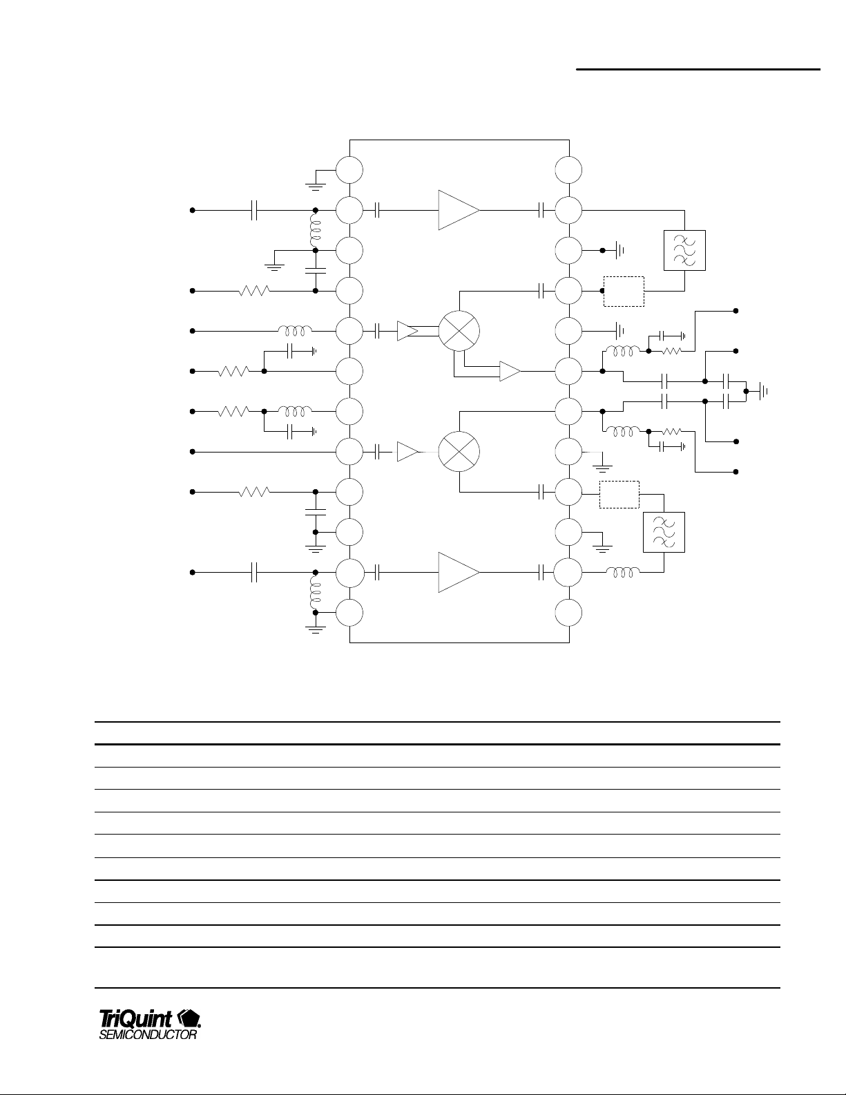
Application/Test circuit
TQ9222
Data Sheet
LNA in B
V LNA B
LO in B
V MX B
V MX A
LO in A
V LNA A
LNA in A
R4
R2
R5
R1
C1
C6
C4
C3
C2
1
2
L4
3
C5
L3
L2
L1
4
5
6
7
8
9
10
11
12
24
23
22
2
21
20
19
18
17
2
16
15
14
13
N2
L6
L5
L8
N1
1
C7
R6
C8
C11
R3
C10
1
F2
V IF B
IF out B
C9
C12
IF out A
V IF A
F1
TQ9222
Bill of Material for TQ9222 Receiver Application/Test Circuit
Component Reference Designator Part Number Value Size Manufacturer
Receiver IC U1 TQ9222 QSOP-24 TriQuint Semiconductor
Capacitor C1 1.2pF 0603
Capacitor C2, C3, C4, C5 1000pF 0603
Capacitor C6 1.5pF 0603
Capacitor C7, C10
.01µF
Capacitor C9 4.7pF 0603
Capacitor C8, C11 12pF, 10pF 0603
Capacitor C12 8.2pF 0603
Capacitor C13 1.5pF 0603
Capacitor C14, C15 (filter
0.5pF 0603
dependent)
For additional information and latest specifications, see our website: www.triquint.com 5
0603
 Loading...