

TriQuint Semiconductor Inc TQ9203 Datasheet
WIRELESS COMMUNICATIONS DIVISION
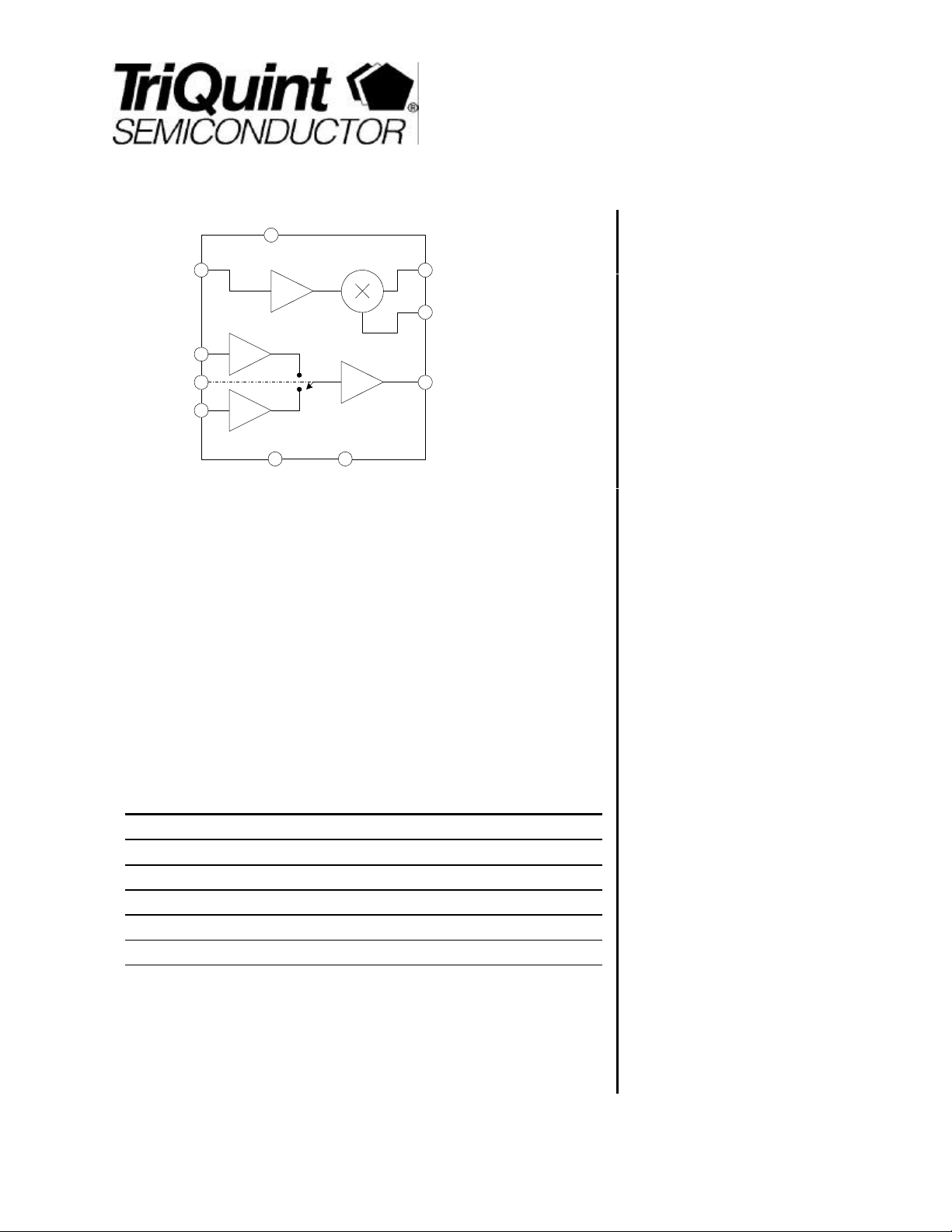
TQ9203
VDD
Mixer
LO In
LNA
IN0
Select
LNA
IN1
GND
LO Tune
Mixer
IF out
Mixer
RF In
LNA
out
Product Description
The TQ9203 RFIC Downconverter is a multifunction RF front end designed for the
high dynamic range cellular communications standards. The design of the TQ9203
provides a 2.5dB system noise figure for excellent sensitivity, and a good signal
range with –10dBm input IP3. Its low current consumption, single +5V operation and
small, plastic surface-mount package are ideally suited for cost-competitive, spacelimited and portable applications. In addition, two selectable RF inputs simplify
implementation of “antenna diversity” in applications such as CDPD. The TQ9203 is
specified over a RF frequency range of 800 to 1000MHz, and therefore may be used
for any of the cellular and cordless telephony standards.
DATA SHEET
Low-Current Cellular
Band Downconverter IC
Features
§ +5-V single supply
§ Internal buffer amplifier on mixer
LO port
§ On-chip matching to 50Ω
§ Two selectable RF inputs
§ Low-cost SO-14 plastic package
§ 21dB system gain
§ -10dBm typical input intercept point
§ 2.5dB typ. system noise figure
§ 10.5mA typ. operating current
Electrical Specifications
Parameter Min Typ Max Units
Frequency 800 1000 MHz
Gain 21.0 dB
Noise Figure 2.5 dB
Input 3rd Order Intercept -10.0 dBm
DC supply Current 10.5 mA
Note 1. Test Conditions: Vdd=5V, Ta=25C, filter IL=3.0dB, RF=881MHz, LO=966MHz, IF=85MHz,
LO input=-6dBm
2. Specified with external noise-matching circuit elements, with image-stripping BPF IL=3dB
3. Frequency separation of the two signals is 500KHz; BPF IL=3dB
1
Applications
§ Cellular Communications
§ Spread-Spectrum Receivers
§ Cordless Phones
Electrical Characteristics
For additional information and latest specifications, see our website: www.triquint.com 1

TQ9203
Data Sheet
Parameter Conditions Min. Typ/Nom Max. Units
RF Frequency Tuned external match 800 1000 MHz
LO Frequency Tuned external match 700 1300 MHz
IF Frequency Tuned external match 30 300 MHz
LO input level -6 dBm
Supply voltage 4.5 5.0 5.5 V
Gain (LNA IN1)
Gain (LNA IN0)
Noise Figure LNA IN0 Pin; SSB
Input 3rd Order Intercept Frequency Sep. = 500KHz -10.0 dBm
Return Loss Mixer RF input
Supply Current 10.5 12 mA
Note 1. Test Conditions:, Vdd=5.0V, Ta=25C, filter IL=3.0dB, RF=881MHz, LO=966MHz, IF=85MHz, LO input=-6dBm: unless otherwise specified.
2. Conversion gain, noise figure, and IP3 assume an image stripping band-pass filter between the LNA section and the Mixer section with a 3dB insertion loss.
LO=-6dBm, RF=-35dBm
LO=-6dBm, RF=-35dBm
LNA IN1 Pin; SSB
Mixer LO input
LNA OUT Return Loss
18.0 21.0
21.0
2.8
2.5 3.0
10
10
20
dB
dB
dB
dB
dB
dB
dB
Electrical Characteristics-LNA section only
Parameter Conditions Min. Typ/Nom Max. Units
Gain RF=-40dBm 18.0 dB
Noise Figure LNA0 Active
LNA1 Active
Input 3rd Order Intercept Separation: 500KHz +13.0 dBm
Output Gain Compression 1.5 dBm
Off Isolation, LNA In1/Out
Off Isolation, LNA In0/Out
Reverse Isolation 38.0 dB
Supply Voltage 4.5 5.0 5.5 V
Supply Current Mixer Off
Note 1. Test Conditions:, Vdd=5.0V, Ta=25C, RF=881MHz.
2. Vdd pin supplies connect to both the LNA and the LO buffer amps. Mixer cannot operate without Vdd connection. Mixer Vdd through the IF pin connects
only to the mixer FET.
Select=0V, LNAo On
Select=5C, LNA1 On
(2)
Powered down 8.8 mA
2.1
1.8
-7
-5
dB
dB
dB
dB
2 For additional information and latest specifications, see our website: www.triquint.com
TQ9203
Data Sheet
Electrical Characteristics- Mixer section only
Parameter Conditions Min. Typ/Nom Max. Units
Conversion Gain 0 dB
Noise Figure 12.0 dB
Output 3rd Order Intercept 10.0 dBm
Mixer RF Return Loss 15.0 dB
Mixer LO Return Loss 10.0 dB
LO Input Power -6.0 dBm
LO to IF Isolation 40.0 dB
LO to RF Isolation 5.0 dB
RF to IF Isolation 40.0 dB
Supply Current 4.0 mA
Note 1: Test Conditions:, Vdd=5.0V, Ta=25C, filter IL=3.0dB, RF=881MHz, LO=996MHz, IF=85MHz, LO input=-6dBm: unless otherwise specified.
-Absolute Maximum Ratings
Parameter Value Units
DC Power Supply 8.0 V
RF Input Power +10 dBm
Operating Temperature -40 to 85 C
Storage Temperature -55 to 150 C
For additional information and latest specifications, see our website: www.triquint.com 3

TQ9203
Gain vs. Freq. vs. Temp.
Data Sheet
Typical Performance
Test Conditions (Unless Otherwise Specified): Vdd=5.0V, Ta=25C, filter IL=3.0dB, RF=881MHz, LO=996MHz, IF=85MHz, LO input=-6dBm
Conversion Gain vs. Freq. vs. Temp.
23
22
21
20
19
18
Gain (dB)
17
16
15
14
869 872 875 878 881 884 887 890 893
Freq. (MHz)
Input IP3 vs. Freq. vs. Temp.
-6
-7
-8
-9
Input IP3 (dB)
-10
-11
-12
869 872 875 878 881 884 887 890 893
Freq. (MHz)
-40C
+25C
+85C
-40C
+25C
+85C
LNA Performance
Noise Figure vs. Freq. vs. Temp.
3
2.5
2
1.5
1
Noise Figure (dB)
0.5
0
869 872 875 878 881 884 887 890 893
Freq. (MHz)
LNA Performance
19
18
17
16
Gain (dB)
15
14
13
12
869 872 875 878 881 884 887 890 893
Freq. (MHz)
+85C
+25C
-40C
-40C
+25C
+85C
4 For additional information and latest specifications, see our website: www.triquint.com
Noise Figure vs. Freq. vs. Temp.
4
3.5
3
2.5
2
1.5
1
Noise Figure (dB)
0.5
0
869 872 875 878 881 884 887 890 893
Freq (MHz)
+85C
+25C
-40C
LNA Performance
IP3 vs. Freq. vs. Temp.
13.5
13
12.5
12
Input IP3 (dB)
11.5
11
869 872 875 878 881 884 887 890 893
Freq. (MHz)
-40C
+25C
+85C
 Loading...