

TriQuint Semiconductor Inc TQ9147B Datasheet
WIRELESS COMMUNICATIONS DIVISION
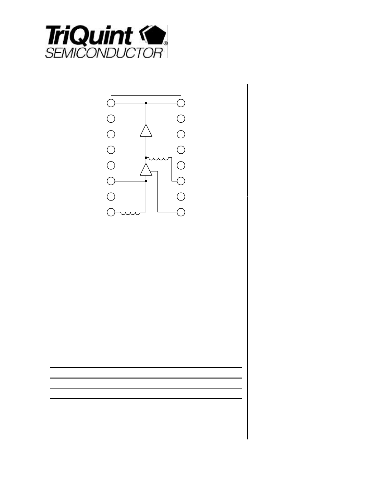
TQ9147B
RF
GND
GND
GND
GND
RF
GND
V
OUT
1 16
2
3
4
5
6
IN
7
G1
RF
OUT
15
GND
14
GND
13
GND
GND
12
11
V
G2
10
GND
98
V
D1
Product Description
The TQ9147 is a high efficiency two stage GaAs MESFET power amplifier IC
intended for use in AMPS (IS-19) applications that operate in the US Cellular (824 849 MHz) band. The TQ9147 requires minimal external RF circuitry and operates
from a 4.8-Volt supply. With its flexible, off-chip, single component output matching
circuit, the TQ9147 is suitable for use in other applications near the cellular band,
such as 900 MHz ISM applications.
The TQ9147 utilizes a space saving SO-16 plastic package that minimizes board
area and cost.
DATA SHEET
2-Stage AMPS
Power Amplifier IC
Features
§ High Efficiency
§ +32 dBm Output Power
§ 50Ω Matched Input
§ SO-16 Plastic Package
§ Monolithic Power Amp
Applications
§ AMPS Mobile Phones
§ CDPD Modems
§ General ISM Band Applications
Electrical Specifications
Parameter Min Typ Max Units
Output Power +31.5 +32 dBm
Efficiency 55 60 %
Note 1: Test Conditions: VDD = 4.8 V, PIN = +7 dBm, Freq. = 824 & 849 MHz, TC = 25° C,
Min/max values 100% production tested.
1
Electrical Characteristics
For additional information and latest specifications, see our website: www.triquint.com 1
TQ9147B
Data Sheet
Electrical Characteristics
Parameter
Frequency tuned for cellular band 824 849 MHz
Supply Voltage (VDD)
Temperature measured at case -40 25 +110
P
OUT
Efficiency 55 60 %
Rx band Noise
Small Signal Gain PIN = -10 dBm 32 dB
Power Gain P
Input Return Loss PIN = -30 to +7 dBm 10 dB
Harmonics
4th Harmonic
Spurious (Stability) PIN = -30 to +7 dBm -70 dBc/30 kHz
RF Off Isolation 20 dBc
Ruggedness VDD at burnout 6.5 V
Note 1: Test Conditions: VDD = 4.8 V, PIN = +7 dBm, Freq. = 824 & 849 MHz, VGG = 3.5 V, TC = 25° C.
Note 2: Noise power is measured in 30 kHz band width at the transmit frequency plus 45 MHz
Note 3: Load is set to 50 ohms, output power measured at nominal test conditions. Load VSWR is set to 10:1 and the angle is varied 360 degrees over 5 seconds.
1
Conditions Min Typ/Nom Max Units
2.7 4.8 6.0 V
2
2nd Harmonic
3rd Harmonic
VDD = 4.8 V
VDD = 4.3 V
PIN = -30 to +7 dBm -90 dBm
= 32 dBm (typ) 25 dB
OUT
31.5 32
30
-30
-35
-35
Load set to 50 ohms, output power remeasured and compared with the first measurement to check for no degradation from the first measurement.
o
C
dBm
dBm
dBc
dBc
dBc
Absolute Maximum Ratings
Parameter Value Units
DC Power Supply
1
8.0 V
DC Gate Voltage -5.0 V
RF Input Power 20 dBm
Storage Temperature -55 to 150
Operating Temperature (case) -40 to 110
Note 1: Into a 10:1 mismatch.
° C
° C
2 For additional information and latest specifications, see our website: www.triquint.com
TQ9147B
Data Sheet
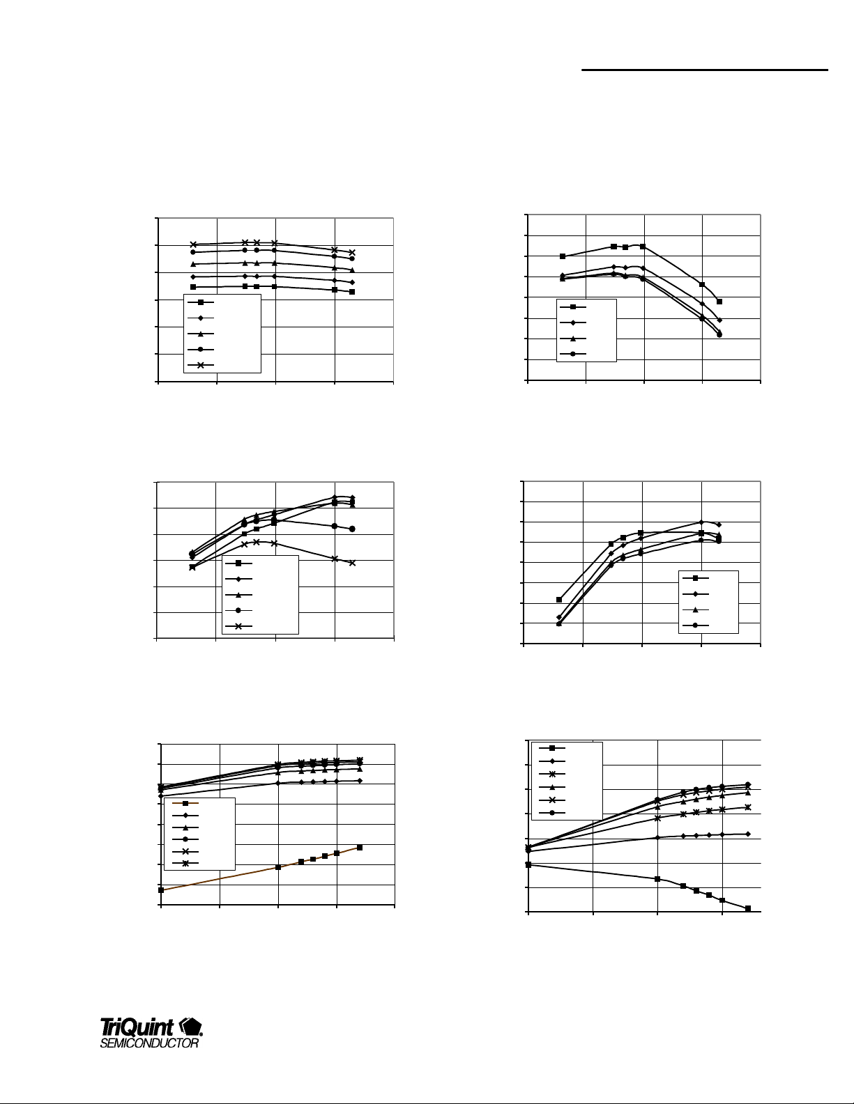
Typical Performance
Test Conditions (Unless Otherwise Specified): VDD = 4.8 V, PIN = +7 dBm, Freq. = 824 & 849 MHz, TC = 25° C, constant gate
voltages: VG1 = -1.5 V, VG2 = -2.2 V.
Output Power vs. Frequency and VDD
40
35
30
25
POUT (dBm)
20
15
VDD=3.0 V
VDD=3.6 V
VDD=4.6 V
VDD=5.8 V
VDD=7.0 V
10
750 800 850 900 950
Frequency (MHz)
Efficiency vs. Frequency and VDD
70
65
60
55
50
Efficiency (%)
45
VDD=3.0 V
VDD=3.6 V
VDD=4.6 V
VDD=5.8 V
VDD=7.0 V
40
750 800 850 900 950
Frequency (MHz)
Output Power vs. Frequency vs. Temp.
33.0
32.5
32.0
31.5
31.0
30.5
Pout (dBm)
30.0
29.5
-30 C
25 C
85 C
110 C
29.0
750 800 850 900 950
Frequency (MHz)
Efficiency vs. Frequency vs. Temp
70
68
66
64
62
60
Efficiency ( % )
58
56
-30 C
25 C
85 C
110 C
54
750 800 850 900 950
Freq ( MHz )
Output Power vs. Input Power vs. VD1
40
30
20
10
0
-10
POUT (dBm)
-20
Vd1=0V
Vd1=1V
Vd1=2V
Vd1=3V
Vd1=4V
Vd1=5V
-30
-40
-10 -5 0 5 10
PIN (dBm)
For additional information and latest specifications, see our website: www.triquint.com 3
Efficiency vs. Input Power vs. Vd1
100
80
60
40
Vd1=0V
Vd1=1V
Vd1=2V
Vd1=3V
Vd1=4V
Vd1=5V
20
Efficiency (%)
0
-20
-40
-10 -5 0 5
PIN (dBm)
 Loading...