

TriQuint Semiconductor Inc TQ9132B Datasheet
WIRELESS COMMUNICATIONS DIVISION
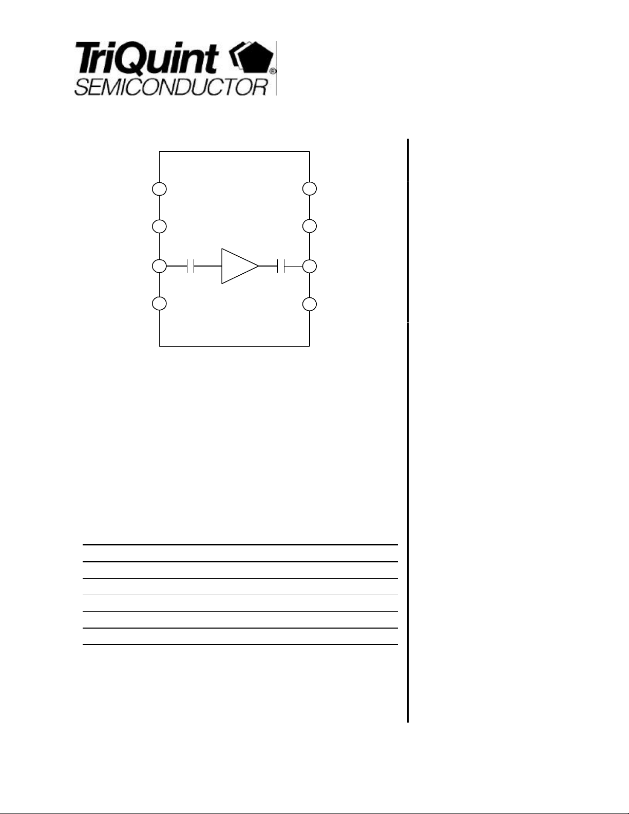
TQ9132B
VDD
1
DATA SHEET
GND
8
GND
GND GND
IN
2
3
4
GND
7
6
OUT
5
TQ9132B
Product Description
The TQ9132B amplifier is an 800-2500 MHz amplifier capable of providing moderate
output power (50 mW) for a wide variety of transmit and receive applications. The
amplifier’s input and output are matched to 50 Ω with internal circuitry, simplifying
interfaces to 50 Ω systems. In addition, DC blocking capacitors are included on chip,
permitting direct connections to the input and output. Its 8-pin surface mount
package and low cost are well suited to many wireless communications applications.
Electrical Specifications
1
3V Cellular TDMA/AMPS
Power Amplifier IC
Features
§ Single 3V- 6V supply
§ Wide frequency range
§ +17 dBm output power
§ Input and output matched to 50 Ω
§ SO-8 surface mount plastic package
Applications
§ Power Amplifier drivers
§ PCN Medium-power amplifiers
§ Medium-power WLANs
Parameter Min Typ Max Units
Gain 13.5 16 dB
Output 1 dB Gain Compression 15.5 17 dBm
Input Return Loss 12 dB
Output Return Loss 12 dB
DC Supply Current 85 100 MA
Note 1: Test Conditions: VDD = 5.0 V, Freq. = 2500 MHz, TA= 25° C.
Note 2: . Min/max values 100% production tested
Electrical Characteristics
For additional information and latest specifications, see our website: www.triquint.com 1
§ CDPD Modems
§ Base Station receivers
TQ9132B
Data Sheet
Electrical Characteristics
Parameter Conditions Min. Typ/Nom Max. Units
Frequency 800 800 to 2500 2500 MHz
Supply Voltage (VDD)
Gain 13.5 16 dB
Noise Figure 4.1 dB
Output 1 dB Gain Compression 15.5 17 dBm
Output 3rd Order Intercept 27 dBm
Input Return Loss 12
Output Return Loss 12 10 dB
DC Supply Current 85 100 mA
Note 1: Test Conditions: VDD = 5.0 V, Freq. = 2500 MHz, TA= 25° C.
Note 2: . Min/max values 100% production tested
Absolute Maximum Ratings
3.0 5.0 6.0 V
10
dB
Parameter Value Units
DC Power Supply 7.0 V
Power Dissipation 500 mW
Input Power +10 dBm
Storage Temperature -55 to 150
Operating Temperature (case) -40 to 70
Thermal Resistance 135.5
° C
° C
o
C/W
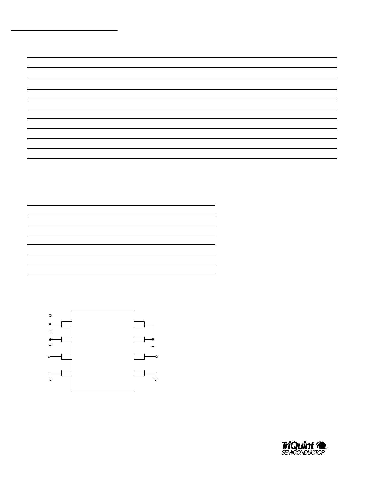
Application/Test Circuit
VDD
0.01 µF
Input
1
2
GND
TQ9132B
3
IN
GND GND
4
GND
GND
OUT
8VDD
7
6
5
Output
2 For additional information and latest specifications, see our website: www.triquint.com
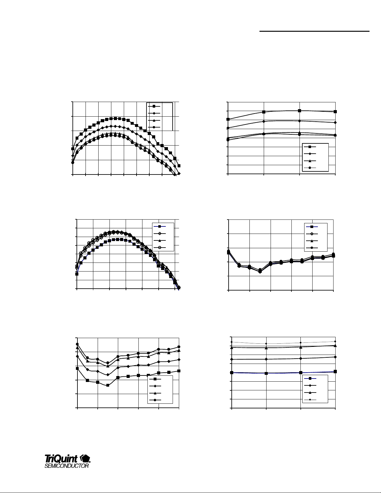
Typical Performance
Gain vs. Frequency vs. Vdd
Test Conditions (Unless Otherwise Specified): VDD = 5 V, Freq. = 2500 MHz, TC = 25° C.
TQ9132B
Data Sheet
Gain vs. Frequency vs. Temperature (Vdd = 5V)
22
20
18
16
Gain (dB)
14
12
500 800 1100 1400 1700 2000 2300 2600 2900
Frequency (MHz)
20
19
18
17
16
Gain (dB)
15
14
13
12
500 900 1300 1700 2100 2500 2900
Frequency (MHz)
-40 C
25 C
70 C
85 C
3 V
4V
5V
6V
Gain vs. Vdd vs. Temperature (1900 MHz)
20
19
18
17
16
Gain (dB)
15
14
13
12
3.0 4.0 5.0 6.0
Vdd (V)
NF vs. Frequency vs. Vdd
8.0
7.0
6.0
NF (dB)
5.0
4.0
3.0
500 1000 1500 2000 2500 3000
Frequency (MHz)
-40 C
25 C
70 C
85 C
3 V
4 V
5 V
6 V
NF vs. Frequency vs. Temperature
7.0
6.0
5.0
4.0
NF (dB)
3.0
2.0
500 1000 1500 2000 2500 3000
Frequency (MHz)
For additional information and latest specifications, see our website: www.triquint.com 3
-40 C
25 C
70 C
85 C
NF vs. VDD vs. Temperature
6.5
6.0
5.5
5.0
4.5
NF (dB)
4.0
3.5
3.0
2.5
3.0 4.0 5.0 6.0
VDD (V)
-40 C
25 C
70 C
85 C
 Loading...