

TriQuint Semiconductor Inc TQ8106S, TQ8105S, TQ8106P, TQ8105P Datasheet
T R I Q U I N T S E M I C O N D U C T O R , I N C .
1
PRELIMINARY DATA SHEET
For additional information and latest specifications, see our website: www.triquint.com
TELECOM
PRODUCTS
The TQ8105/TQ8106 are SONET/SDH transceivers that integrate
multiplexing, demultiplexing, SONET/SDH framing, clock-synthesis PLL, and
enhanced line and clock diagnostic functions into a single monolithic device.
The TQ8106 is a pin-compatible upgrade of the TQ8105 that includes a
Clock and Data Recovery (CDR) function. The TQ8105 and TQ8106 allow
maximum flexibility in the selection of internal/external Clock and Data
Recovery, Opto-Electronic (O/E) Module, and Reference Clock Sources.
On-chip PLLs use external RC-based loop filters to allow custom tailoring of
loop response and support the wide range of reference clock frequencies
found in SONET/SDH/ATM systems. For transmit clock synthesis or for CDR,
the PLLs exceed ANSI, Bellcore, and ITU jitter specifications for systems
when combined with industry-typical O/E devices such as Sumitomo, AT&T,
HP, and AMP. The TQ8105/TQ8106 PLLs provide byte clocks and constantrate 38.88 MHz and 51.84 MHz, synthesized clock outputs, providing
clocking for UTOPIA and other system busses. Transmit data may also be
clocked into the devices with respect to the reference clock.
Operating from a single +5V supply, the TQ8105/TQ8106 provides fully
compliant functionality and performance, utilizing direct-connected PECL
levels (differential or single-ended) for high-speed I/O. As compared to ACcoupled schemes, the direct-coupled connections reduce jitter and
switching-level offsets due to data patterns. The TQ8105/TQ8106 can also
provide direct connection to high-speed I/O utilizing ECL levels with a –5V
supply. Low-speed bus, control, and clock I/O utilize TTL levels. (An ECL/
PECL reference clock input is also provided; at 155.52 MHz the input should
be only PECL/ECL.) Output TTL pins can be tristated and may also be
configured for V
OH
with a 3.3V supply connection.
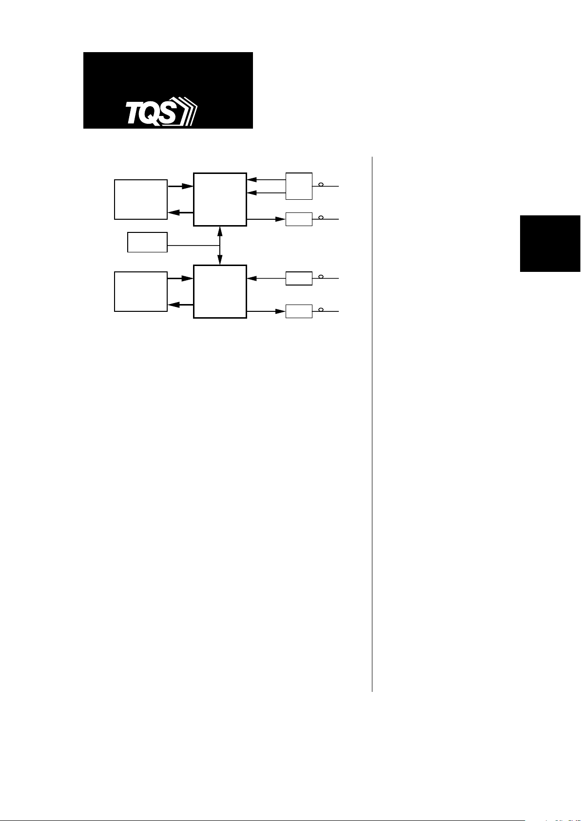
TQ8105/8106
SONET/SDH
Overhead
Processor
TQ8105
or
TQ8106
SONET/SDH
Transceiver
Tx O/E
Rx O/E
with
CDR
SONET/SDH
Overhead
Processor
TQ8106
SONET/SDH
Transceiver
with CDR
Tx O/E
Rx O/E
Reference
Clock
SONET/SDH
Transceivers
Features
• Single-chip, byte-wide Mux,
Demux, Framer, and Tx clocksynthesis PLL with enhanced
diagnostics
• TQ8106 includes monolithic
Clock and Data Recovery
• SONET/SDH/ATM compliant for
STS-12/STM-4 (622 Mb/s) or
STS-3/STM-1 (155 Mb/s) rates
• 155.52, 77.76, 51.84, 38.88, or
19.44 MHz reference clock inputs
with TTL, PECL, or ECL level
• 38.88 MHz and 51.84 MHz clock
outputs for UTOPIA as well as
byte clock rate (77.76 or 19.44 MHz)
• External RC-based loop filters
• Integrated loopbacks with
enhanced line and reference
clock diagnostics
• Direct-coupled standard, PECL,
high-speed I/O with ECL option
• Clean TTL interface to
PMC-Sierra devices
• 100-pin 14x14 mm JEDEC
plastic package
• +5V-only supply for PECL I/O
(–5.2V required for ECL I/O option)
• –40 to +125°C case operating
temperature
2
TQ8105/TQ8106
PRELIMINARY DATA SHEET
For additional information and latest specifications, see our website: www.triquint.com
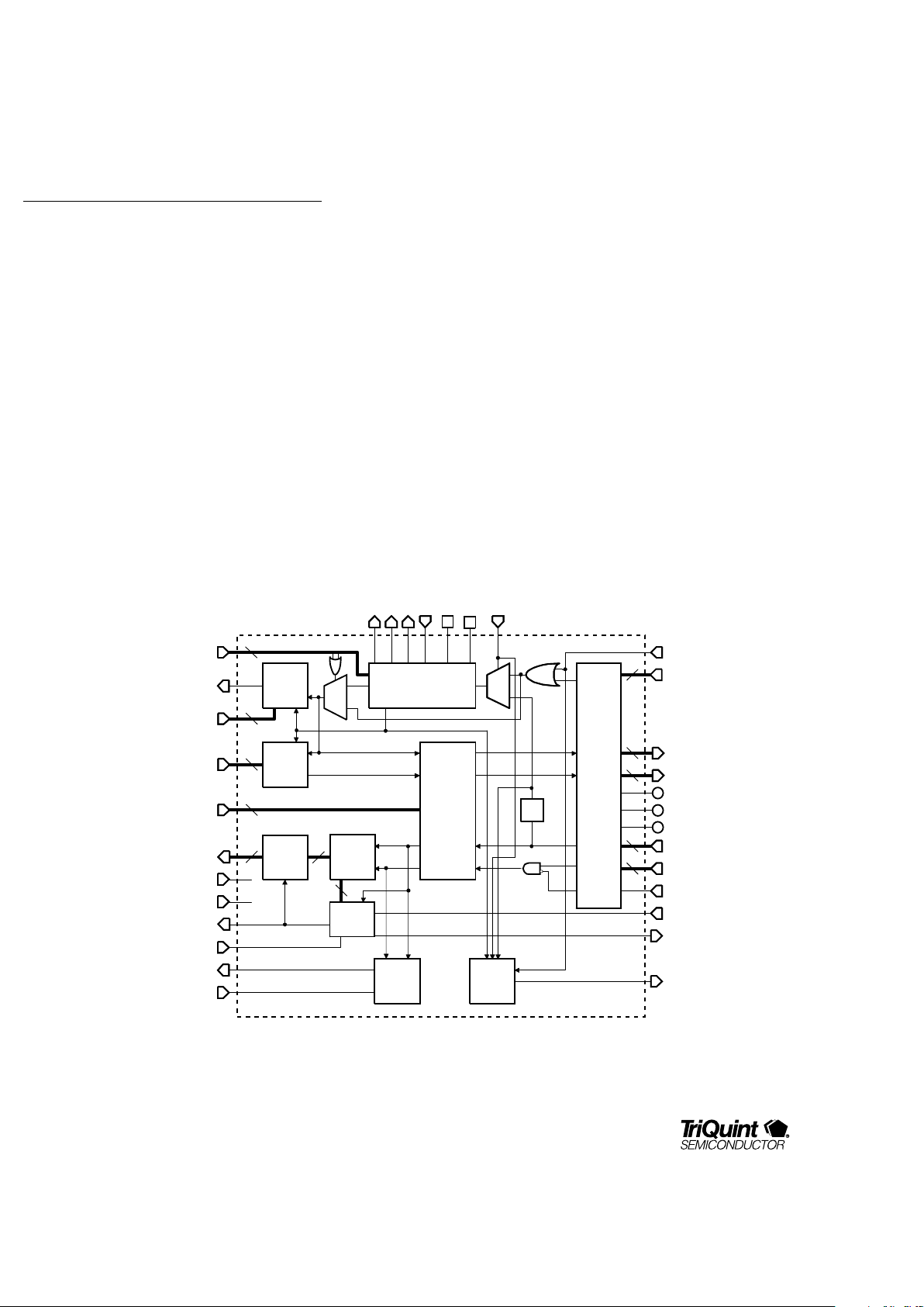
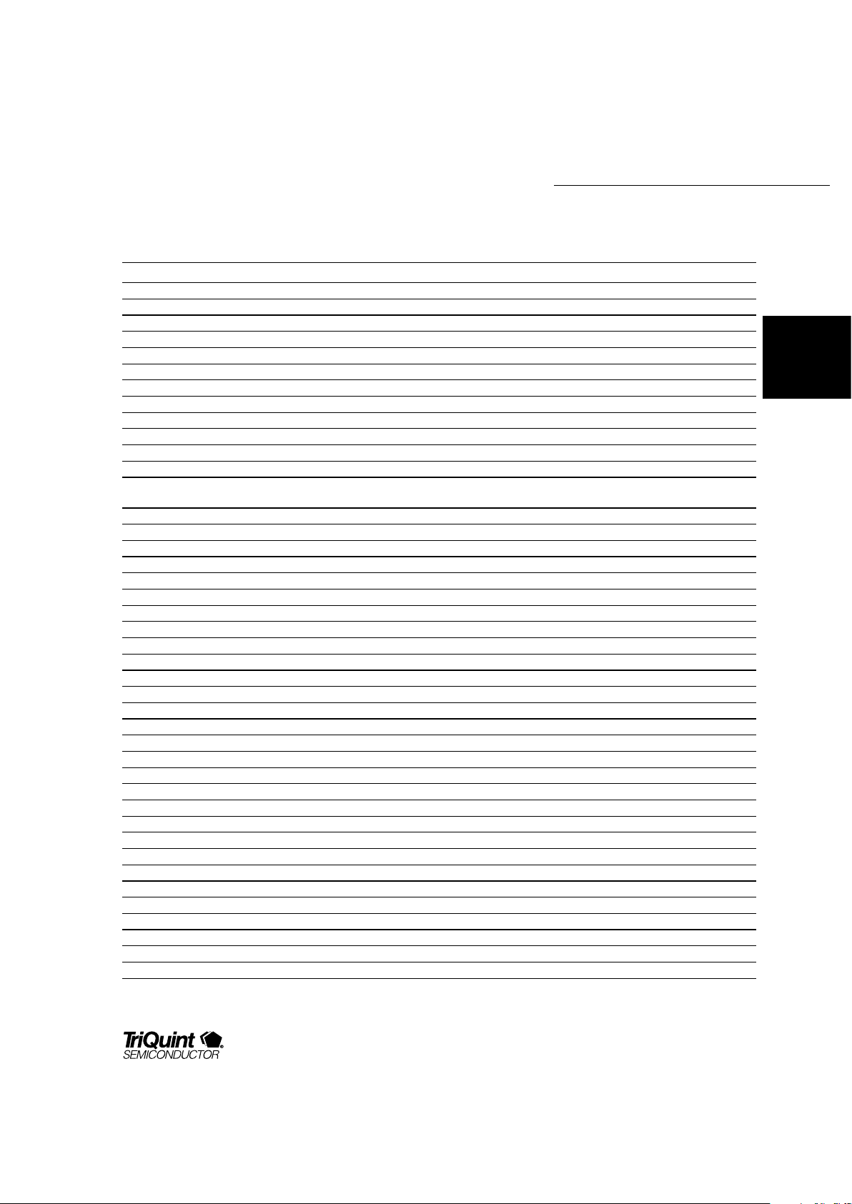
Figure 1. TQ8105 Block Diagram
The combination of a thermally enhanced, 100-pin
JEDEC, metric, plastic package, the low-power
dissipation of the device, and the wide casetemperature range permits operation without a heat
sink in most designs.
The TQ8106 uses the same pinout as the TQ8105 and
is compatible with it.
The TQ8105/TQ8106 provides comprehensive,
integrated, loopback functionality and enhanced line
and reference clock diagnostics required of SONET/
SDH systems, minimizing additional external circuitry.
TQ8105/TQ8106 diagnostics include:
• Loss of Reference clock detector (LOR) output to
indicate that the PLL Reference Clock is not toggling
• Lock Indicator (RLOCK), which permits monitoring
of the receiver clock frequency, flagging when the
frequency drifts beyond approximately 500 ppm
• Loss of Signal (LOS) detector output to indicate that
the incoming data stream has no data transitions in
128-bit periods
• ECL/PECL input (NSOL) to allow LOS from an O/E
module to force the data stream to all zeroes,
eliminating the need for external glue logic.
CKSRC(2:0)
MXD(7:0)
TXD
TXCK
RXD
RXCK
2
2
2
2
ECL/
PECL
I/O
Block
DVPP
8
Parallel
to
Serial
DXD(7:0)
8
LBM(1:0)
2
PH(1:0)
2
Loop
Back &
Retime
Block
LOS
Detect
VPP
VNN
FP1
REFCKE
2
REFCKT
B
Y
A
B
Y
A
MMS
Clock
Data
Clock
Data
Clock
Data
Clock
Data
/8
Ext. Clk
OC3
11
Hold
Register
NOE
LOS
DXSYNC
OOF
8
Serial
to
Parallel
Clock
Phase
TxBC
RxBC
Framer
Clock/8
LOR
NRESET
SDHCK
3
PLL Clock
Synthesizer
FP2
NSOL
SONETC
K
CLRLOS
Freq.
Lock
Detect
RLOCK
FRPWR
TQ8105
TQ8105/TQ8106
3
PRODUCTS
PRELIMINARY DATA SHEET
For additional information and latest specifications, see our website: www.triquint.com
TELECOM
PRODUCTS
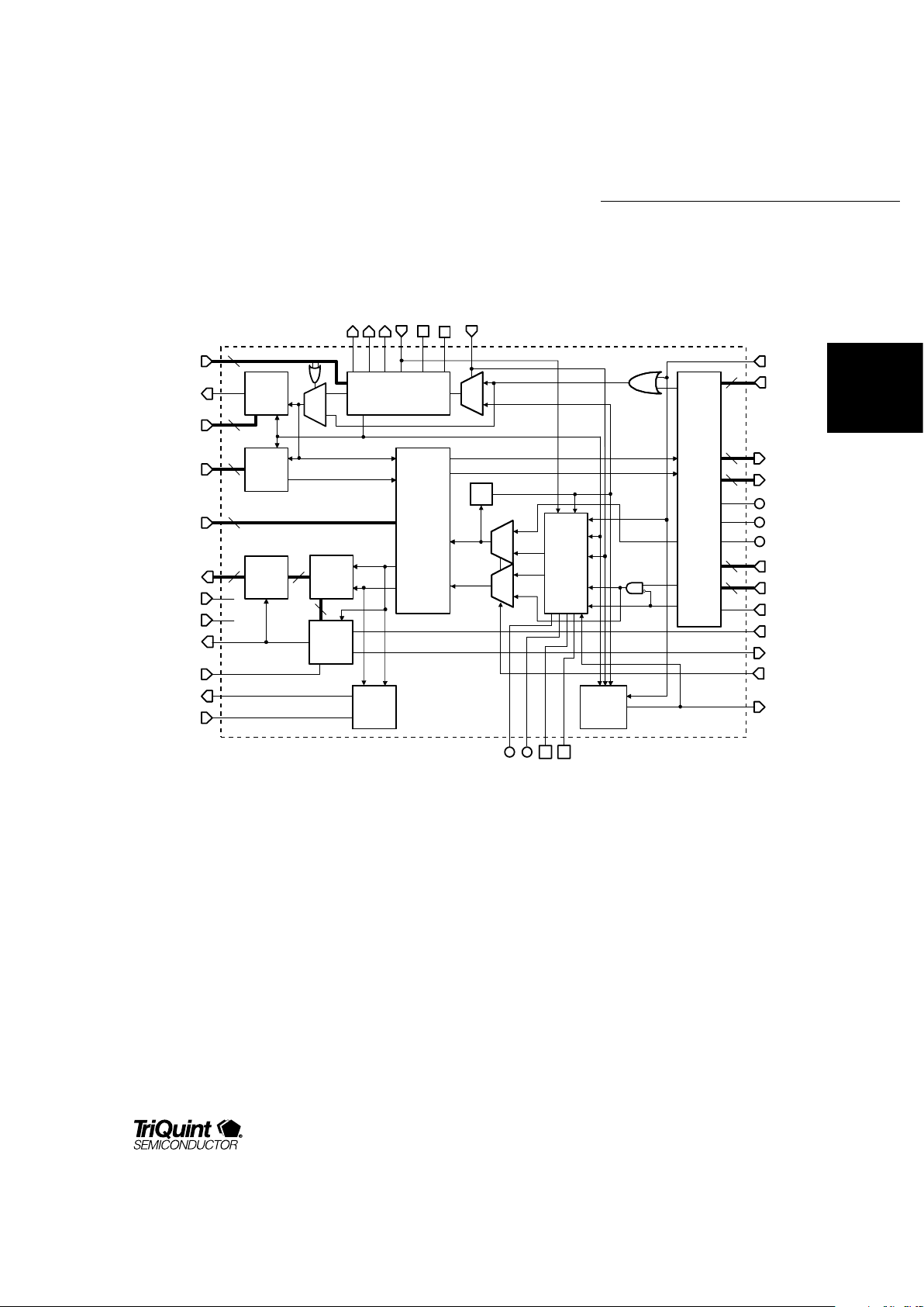
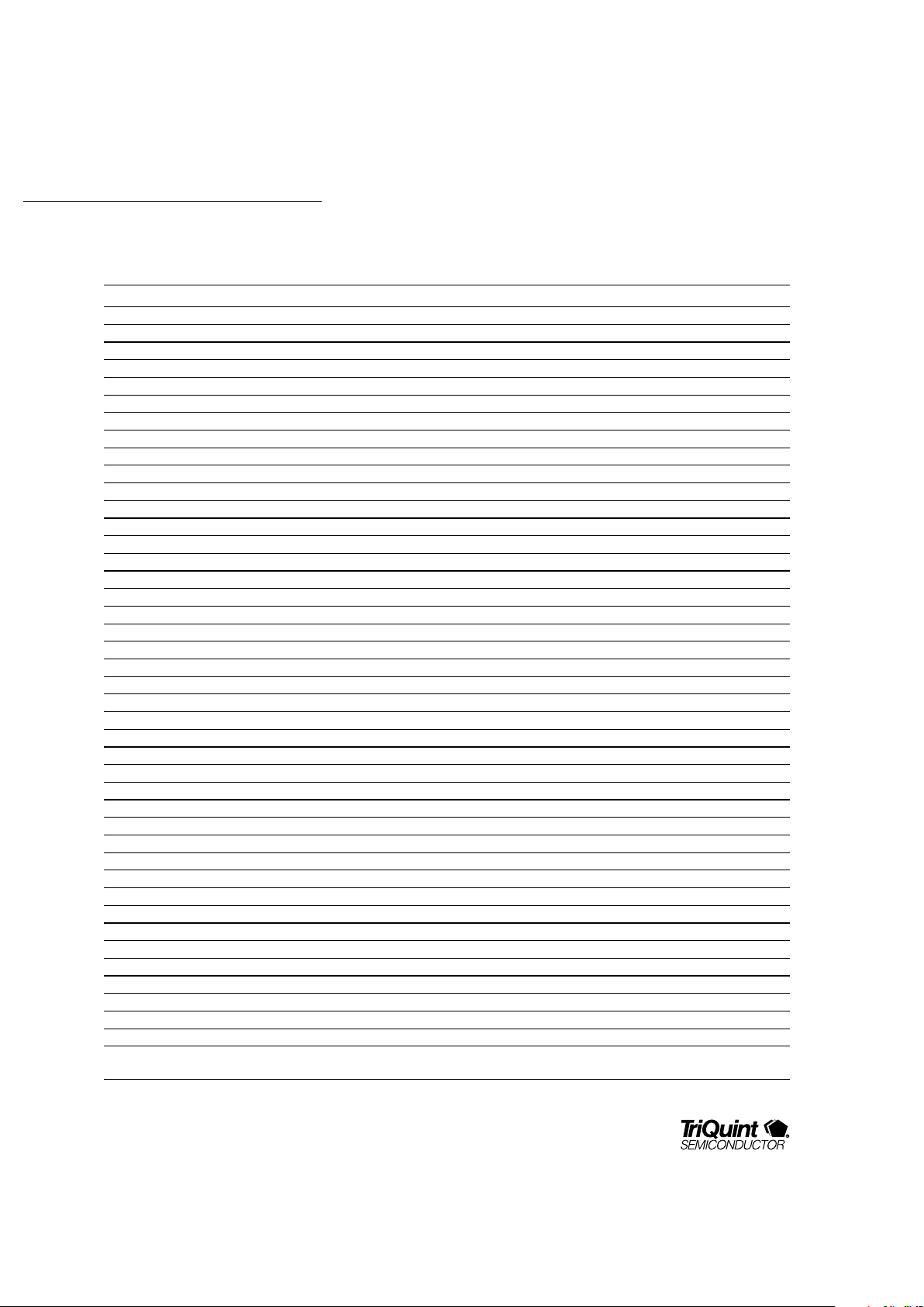
Figure 2. TQ8106 Block Diagram
CKSRC(2:0)
MXD(7:0)
TXD
TXCK
RXD
RXCK
2
2
2
2
ECL/
PECL
I/O
Block
DVPP
8
Parallel
To
Serial
DXD(7:0)
8
LBM(1:0)
2
PH(1:0)
2
Loopback
& Retime
Block
LOS
Detect
VPP
VNN
FP1
REFCKE
2
REFCKT
B
Y
A
MMS
Clock
Data
Clock
Data
Clock
Data
Clock
Data
/8
Ext. Clk
OC3
11
Hold
Register
NOE
LOS
DXSYNC
OOF
8
Serial
To
Parallel
Clock
Phase
TxBC
RxBC
Framer
Clock/8
LOR
NRESET
SDHCK
3
PLL Clock
Synthesizer
FP2
NSOL
SONETCK
CLRLOS
Freq.
Lock
Detect
RLOCK
FRPWR
B
Y
A
B
Y
A
B
Y
A
Clock
& Data
Recovery
Data
Clock
NCDREN
CDRFP2
CDRFP1
CDRGND
CDRAVDD
Clock
Data
TQ8106
4
TQ8105/TQ8106
PRELIMINARY DATA SHEET
For additional information and latest specifications, see our website: www.triquint.com
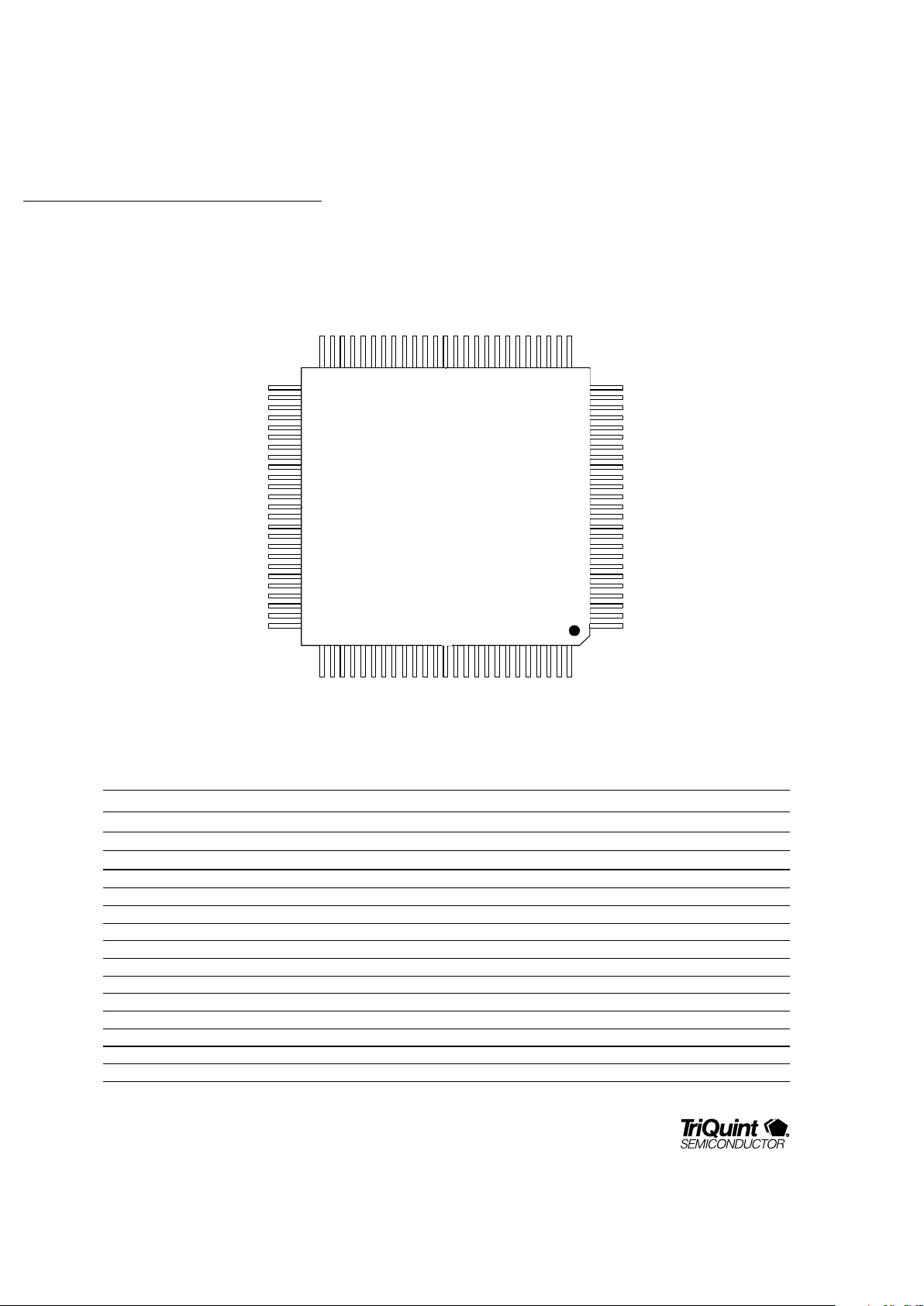
Figure 3. 100-Pin Enhanced Plastic 14x14 mm Package Pinout
Table 1. Signal Descriptions (continues on next page)
Pin Signal Function Description
1 VNN –5.2V/Ground ECL/PECL section power
2 NC No Connect Do not connect
3 VPP Ground/+5V ECL/PECL Positive Supply (see Table 6B)
4 DVPP Ground/+5V ECL/PECL Driver Return (see Table 6B)
5 REFCKEN ECL/PECL Input Tx Ref. Clock or Bypass Clock, Complement
6 REFCKEP ECL/PECL Input Tx Ref. Clock or Bypass Clock, True
7 DVPP Ground/+5V ECL/PECL Driver Return (see Table 6B)
8 TXCKN ECL/PECL Out Transmit Clock, Complement
9 TXCKP ECL/PECL Out Transmit Clock, True
10 DVPP Ground/+5V ECL/PECL Driver Return (see Table 6B)
11 TXDN ECL/PECL Out Transmit Data, Complement
12 TXDP ECL/PECL Out Transmit Data, True
13 DVPP Ground/+5V ECL/PECL Driver Return (see Table 6B)
14 RXDN ECL/PECL Input Receive Data, Complement
15 RXDP ECL/PECL Input Receive Data, True
Note: *TQ8106-specific signal
Note: *TQ8106-specific signal
13
TXDP
14
15
12
TXDN
11
DVPP
18
RXDP
19
DVPP
20
RXCKP
17
RXDN
16
DVPP
23
NSOL
24
VNN
25 GND
22
DVPP
21
RXCKN
8
DVPP
9
TXCKN
10
TXCKP
7
63REFCKEP
4
VPP
5
REFCKEN
21NC
38
DXD2
39
DGND
40
DXD337VCC36DXD1
43
DGND
44
DXD5
45 VCC
42 DXD4
41
VCC
48 DXD7
49 SVDD
50
VDD47DGND
46 DXD6
33 VCC
34 DXD0
35 DGND
32
DXSYNC
31 DGND
28
NC/CDRAVDD*29VCC30RXBC
27 VDD
26
SVDD
63
VDD
62
LBM0
61
GND
64
NOE
65
GND
58
RLOCK
57
56
CLRLOS
59
CDRGND*/NC
60
LBM1
53
VCC
52
OOF
51
GND
54
LOS
55
DGND
68
MMS
67
OC3
66
NRESET
69
CKSRC2
70
CKSRC1
73
PH0
72
PH1
71
CKSRC0
74
VDD
75
SVDD
88
DGND
87
TXBC
86
VCC
89
SONETCK
90
VCC
83
MXD5
82
MXD4 81
MXD384MXD685MXD7
78
MXD0 77
76
79
MXD180MXD2
93
LOR
92
DGND
91
SDHCK
94
AGND
95
FP2
98
VDD
97
AVDD
96
FP1
99
REFCKT
100
GND
DVPP
NC/CDRFP2*
NC/CDRFP1*
VPP
GND
VNN
FRPWR
NCDREN*/NC
TQ8105/TQ8106
5
PRODUCTS
PRELIMINARY DATA SHEET
For additional information and latest specifications, see our website: www.triquint.com
TELECOM
PRODUCTS
Table 1. Signal Descriptions (continued)
Pin Signal Function Description
16 DVPP Ground/+5V ECL/PECL Driver Return (see Table 6B)
17 RXCKP ECL/PECL Input Receive Clock, True (Ignored when CDR used)
18 RXCKN ECL/PECL Input Receive Clock, Complement (Ignored when CDR used)
19 DVPP Ground/+5V ECL/PECL Driver Return (see Table 6B)
20 VPP Ground/+5V ECL/PECL Positive Supply (see Table 6B)
21 NSOL ECL/PECL Input Loss of Signal — zeroes serial data in when low; RXBC=TXCK/8
22 VNN –5.2V/Ground ECL/PECL section power (see Table 6B)
23 NC/CDRFP1* Analog Output CDR Loop Filter Pin 1 — Charge Pump Out (ignored by TQ8105)
24 NC/CDRFP2* Analog Input CDR Loop Filter Pin 2 — VCO Tune (ignored by TQ8105)
25 GND GND Core Ground
26 SVDD +5V Output Driver Internal Positive Supply
27 VDD +5V Core Positive Supply
28 CDRAVDD* Analog +5V TQ8106 CDR Analog +5V Supply
(not connected if CDR not used; ignored by TQ8105)
29 VCC +5V/+3.3V TTL Driver Positive Supply
30 RxBC Tristate TTL Out Demultiplexer Byte Clock
31 DGND GND TTL Driver Ground
32 DXSYNC Tristate TTL Out Frame Synchronization Signal
33 VCC +5V/+3.3V TTL Driver Positive Supply
34 DXD0 Tristate TTL Out Demultiplexer Data Bit 0 (LSB)
35 DGND GND TTL Driver Ground
36 DXD1 Tristate TTL Out Demultiplexer Data Bit 1
37 VCC +5V/+3.3V TTL Driver Positive Supply
38 DXD2 Tristate TTL Out Demultiplexer Data Bit 2
39 DGND GND TTL Driver Ground
40 DXD3 Tristate TTL Out Demultiplexer Data Bit 3
41 VCC +5V/+3.3V TTL Driver Positive Supply
42 DXD4 Tristate TTL Out Demultiplexer Data Bit 4
43 DGND GND TTL Driver Ground
44 DXD5 Tristate TTL Out Demultiplexer Data Bit 5
45 VCC +5V/+3.3V TTL Driver Positive Supply
46 DXD6 Tristate TTL Out Demultiplexer Data Bit 6
47 DGND GND TTL Driver Ground
48 DXD7 Tristate TTL Out Demultiplexer Data Bit 7 (MSB)
49 SVDD +5V Output Driver Internal Positive Supply
50 VDD +5V Core Positive Supply
51 NC/CDRGND* GND GND for TQ8106 to powerup CDR (ignored by TQ8105)
52 GND GND Core Ground
53 FRPWR TTL Input Framer Power Control (power on when high)
54 OOF TTL Input Out-of-Frame: Initiates Frame Search/Bit Alignment
55 VCC +5V/+3.3V TTL Driver Positive Supply
56 LOS Tristate TTL Output Loss of Signal (high when > 128 bit periods without transitions)
57 DGND GND TTL Driver Ground
Note: *TQ8106-specific signal
6
TQ8105/TQ8106
PRELIMINARY DATA SHEET
For additional information and latest specifications, see our website: www.triquint.com
Table 1. Signal Descriptions (continued)
Pin Signal Function Description
58 CLRLOS TTL Input Active-high Clear LOS output
59 RLOCK Tristate TTL Output Receive Clock meets lock criteria when high
60 LBM1 TTL Input Loopback Mode Control (see Table 3)
61 GND GND Core Ground
62 LBM0 TTL Input Loopback Mode Control (see Table 3)
63 VDD +5V Core Positive Supply
64 NOE TTL Input TTL tristate control (active low to enable)
65 GND GND Core Ground
66 NRESET TTL Input Global Reset (active low)
67 OC3 TTL Input OC3/OC12 Mode Select
68 MMS TTL Input Master/Slave Mode Control
69 CKSRC2 TTL Input Clock Source Select (see Table 3)
70 CKSRC1 TTL Input Clock Source Select (see Table 3)
71 CKSRC0 TTL Input Clock Source Select (see Table 3)
72 PH1 TTL Input TxBC Phase Select (see Table 3)
73 PH0 TTL Input TxBC Phase Select (see Table 3)
74 VDD +5V Core Positive Supply
75 SVDD +5V Output Driver Internal Positive Supply
76 GND GND Core Ground
77 MXD0 TTL Input Multiplexer Data Bit 0 (LSB)
78 MXD1 TTL Input Multiplexer Data Bit 1
79 MXD2 TTL Input Multiplexer Data Bit 2
80 MXD3 TTL Input Multiplexer Data Bit 3
81 MXD4 TTL Input Multiplexer Data Bit 4
82 MXD5 TTL Input Multiplexer Data Bit 5
83 MXD6 TTL Input Multiplexer Data Bit 6
84 MXD7 TTL Input Multiplexer Data Bit 7 (MSB)
85 VCC +5V/+3.3V TTL Driver Positive Supply
86 TxBC Tristate TTL Out Transmit Byte Clock
87 DGND GND TTL Driver Ground
88 SONETCK Tristate TTL Out 51.84 MHz Clock Output
89 VCC +5V/+3.3V TTL Driver Positive Supply
90 SDHCK Tristate TTL Out 38.88 MHz Clock Output
91 DGND GND TTL Driver Ground
92 LOR Tristate TTL Out Indicates Reference Clock is Absent
93 AGND Analog Ground VCO Analog Ground
94 FP2 Analog Output Transmit PLL Loop Filter, Charge Pump Out
95 FP1 Analog Input Transmit PLL Loop Filter, VCO Tune
96 AVDD Analog +5V VCO & Filter Analog VDD Supply
97 VDD +5V Core Positive Supply
98 REFCKT TTL Input Tx Reference Clock or Bypass Clock
99 GND GND Core Ground
100 NC/NCDREN* TTL Input Internal Pull-up, Low = CDR receiver clock; Float = Pin 17/18 Rx Clk
(ignored by TQ8105)
Note:*TQ8106-specific signal
 Loading...