

TriQuint Semiconductor Inc TQ8101-C Datasheet
T R I Q U I N T S E M I C O N D U C T O R , I N C .
TELECOM
PRODUCTS
1
For additional information and latest specifications, see our website: www.triquint.com
TQ8101C
622/155 Mb/s
SONET/SDH MDFP
Features
• Byte-wide Multiplexing,
Demultiplexing, Framing, and
PLL (MDFP) in one device
• Choice of STS-12/STM-4 or
STS-3/STM-1 transmission rates
• Configurable master or slave
reference clock generation and
PLL bypass for external clocking
• 77.76 MHz or 19.44 MHz output
for the multiplexer; 77.76 MHz or
19.44 MHz and 51.84 MHz
output for the demultiplexer
• External RC loop filter
• Pass-through mode and three
loopback modes for enhanced
filed diagnostics
• Frame-synchronous and bytealigned demultiplexer output,
compliant with SONET and SDH
• Search, detect, and recovery of
framing on out-of-frame input
• Standard TTL and differential or
single-ended ECL I/O (except TXCK)
• Tristate TTL output for factory
circuit-board testability
• 68-pin TriQuint MLC controlled-Z
surface-mount package with
integral heat spreader
•
Dual-supply operation (+5V, –5.2V)
•
Low power dissipation (2.3W nom.)
The TQ8101C is a SONET/SDH transceiver that integrates Multiplexing,
Demultiplexing, SONET/SDH Framing, clock synthesis PLL (MDFP), and
loopback functions in a single monolithic integrated circuit. Implementation
with the TQ8101C requires only a simple external RC loop filter and standard
TTL and ECL power supplies. For optimal performance, the TQ8101C MDFP
is packaged in a 68-pin multilayer ceramic (MLC) surface-mount package
with an integral CuW heat spreader. The TQ8101C provides an integrated
solution for physical interfaces intended for use in STS-12/STM-4
(622.08-Mb/s) and STS-3/STM-1 (155.52-Mb/s) SONET/SDH systems.
The TQ8101C meets ANSI, Bellcore, and ITU requirements for a SONET/
SDH device. With a 51.84-MHz reference clock, the phase-locked loop
(PLL) provides 77.76-MHz or 19.44-MHz output for the multiplexer and
77.76-MHz or 19.44-MHz and 51.84-MHz output for the demultiplexer.
Typical SONET/SDH system applications for the TQ8101C include:
• Transmission system transport cards
• Switch and cross-connect line cards
• Repeaters
• ATM physical layer interfaces
• Test equipment
• Add/drop multiplexers
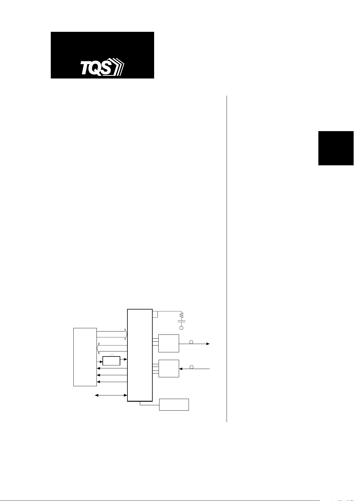
Figure 1. Logical Application
TQ8101C
MDFP
PM5312orPM5355
STTX S/UNI-622
Driver
and
LASER
O/E Rx +
TQ8103
CDR
TOUT(7:0)
OOF
TCLK
RIFP
RICLK
CNTL(3:0)
51.84 MHz
CMOS OSC
MXDT(7:0)
OOF
MXCK0
DXSYNC
DXCK
8-bit data
OC-3 or OC-12
OC-3 or OC-12
RIN(7:0)
MXDT(7:0)
DXDT(7:0)
8-bit data
600 Ω
0.68 µF
V
EE
OHFP
OOF fix*
*Contact PMC-Sierra for
application note.
TQ8101C
2
For additional information and latest specifications, see our website: www.triquint.com
Figure 2. TQ8101C Block Diagram
Figure 3. TQ8101C Package—68-pin MLC
Control
Block
Mux
Serial-to-Parallel
Converter
Loop-
back
Block
PLL Clock
Synthesizer
Mux
Framer
Demux
TXDT
TXCK
RXDT
RXCK
2
2
MXDT(7:0)
CNTL(3:0)
MO
TUNE
IOUT
MXCK(2:0)
MXHC
MXLRC
DXRCK
DXCK
DXDT(7:0)
OOF
DXSYNC
+5V
GND
–5.2V
2
2
TOP V
IEW
1.170
± .006
.950
± .010
.800
4 plcs
Pin 1 index
.050
.016
n
-4 plcs
n
plcs
CuW heat
spreader
1
2
2
33
4
AA
.950
± .010
S
ECTION
A A
.050
.060
± .005
.125.650
± .005
B
OTTOM VIEW
Chip capacitor
4 plcs
Ceramic
or metal
lid
TQ8101C
SONET/SDH/ATM
TELECOM
PRODUCTS
3
For additional information and latest specifications, see our website: www.triquint.com
Functional Description
Figure 2 shows a block diagram of the TQ8101C
multiplexer, demultiplexer, framer, and PLL clock
synthesizer (MDFP). The primary purpose of TQ8101C
is to integrate the conversion of serial and parallel
SONET/SDH data with bit alignment and clock
synthesis in a single device.
Multiplexing
Byte-wide input data on MXDT(7:0)
1
is continuously
strobed into the multiplexer on the rising edge of the
multiplexer clock output, MXCK(2:0).
2
Any of these
three MXCK pins may be used as a reference point for
relative timing. (See Table␣ 8 for setup, hold, and skew
times. See Table␣ 1 for clock selection options.)
Either an on-chip synthesized clock (see “PLL Clock
Synthesis”) or an external high-speed multiplexer
Notes: 1. MXDT(0) is defined as the least significant bit.
2. MXCK(2:0) nominally runs at 77.76 MHz in STS-12/STM-4 mode,
and at 19.44 MHz in STS-3/STM-1 mode.
3. Internal signal. See Figure 5, "TQ8101C Loopback Modes."
4. DXDT (0) is defined as the least significant bit.
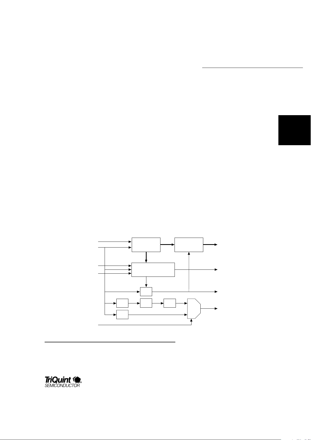
Frame Detection
and Recovery
Shift
Register
Parallel
Register
1
/
3
1
/
8
1
/
2
1
/
2
1
/
3
Mux
DXDTIN
DXHSCK
XFD
OOF
RT
DXDT(7:0)
DXSYNC
DXCK
DXRCK
clock, MXHC, serializes the input data bytes. In the
normal mode of operation, the serial data is then
buffered as ECL-compatible output on TXDT. An ECL
output is provided for the transmit clock, TXCK.
Demultiplexing
As shown in Figure 4, The demultiplexer block converts
incoming serial data on DXDTIN
3
. Byte-wide output
data is presented on DXDT(7:0)
4
slightly after the
falling edge of the output demultiplexer clock, DXCK.
(See Table␣ 8 for setup, hold, and skew times.)
The demultiplexer block also includes clock divider
circuitry, which is used by the demultiplexer to control
divide-by-8 output on DXCK. The MDFP provides a
divide-by-3 or divide-by-12 output, DXRCK.
(See Table 1 for mode selection options.)
Figure 4. Demultiplexer Functional Block
TQ8101C
4
For additional information and latest specifications, see our website: www.triquint.com
Framing
The demultiplexer block (see Figure 2) includes a
frame-detection and recovery block. Regardless of the
state of the OOF input signal, this block takes DXSYNC
high for one period of DXCK whenever it detects a
pattern of three “A1” bytes followed by three “A2”
bytes.
Frame recovery is initiated by the rising edge of the
OOF input signal. The recovery process involves a
search for a bit rotation that satisfies the three-“A1”–
three-“A2” byte pattern specified for SONET/SDH. Once
the pattern is found, DXSYNC goes high and the bit
rotation is synchronized to the correct byte boundaries.
No further byte boundary adjustments are made,
regardless of “A1”-“A2” indication, unless they have
been preceded by an OOF rising edge.
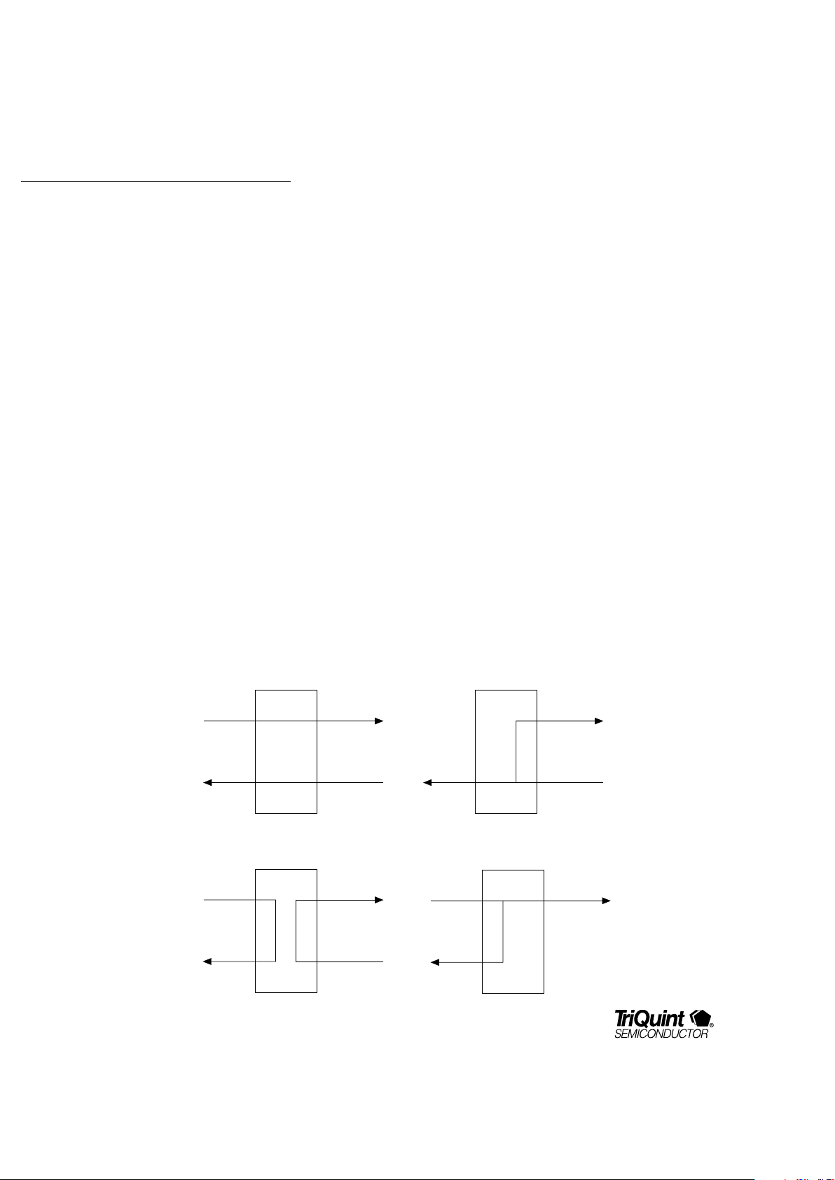
Normal
RXDT
RXCK
TXDT
TXCK
DXDTIN
DXHSCK
MXDTOUT
MXHSCK
Equipment Loopback
TXDT
TXCK
DXDTIN
DXHSCK
MXDTOUT
MXHSCK
Facility Loopback
RXDT
RXCK
TXDT
TXCK
DXDTIN
DXHSCK
Split Loopback
RXDT
RXCK
TXDT
TXCK
DXDTIN
DXHSCK
MXDTOUT
MXHSCK
PLL Clock Synthesis
The PLL utilizes a monolithic voltage-controlled
oscillator with a typical tuning constant of 50 to 100
MHz per volt on the TUNE input. This configuration
provides jitter performance superior to other
technologies. In a typical SONET/SDH application the
TUNE input and charge pump output IOUT are
connected and tied to V
EE
through a 600-ohm resistor
and 0.68-µF capacitor.
Loopback
The TQ8101C features four loopback modes: normal
(pass-through), equipment loopback, split loopback,
and facility loopback. Loopback modes are controlled
by pins CNTL(3:0). Note␣ that the loopback mode does
not affect the latched selection of clock modes and
rates. Note that the RXCK input is␣ directly connected to
the TXCK output in most loopback modes (see below).
Figure 5. TQ8101C Loopback Modes
TQ8101C
SONET/SDH/ATM
TELECOM
PRODUCTS
5
For additional information and latest specifications, see our website: www.triquint.com
Control
The signals on pins CNTL(3:0) can be used to control
the clock rate, clock mode, loopback scheme, and
tristate pins. Also, the internal PLL high-speed clock
may be disabled, allowing an external clock source to
be used on the MXHCN and MXHCP pins.
Note that the NAND tree enable normally is used only
for device testing of the V
IH
and VIL parameters.
Table 1. Modes of Operation
CNTL(3:0) Modes of operation
0h Reset
1h Tristate all TTL outputs except DXRCK and MO
2h NAND-tree test all TTL inputs except CNTL(3:0)
3h DXRCK tristate
4h Frame recovery disable
5h Equipment loopback
6h Facility loopback
7h Split loopback
8h Bypass, slave, internal VCO disabled, STS-3 rate
9h
Bypass, master, internal VCO disabled, STS-3 rate
Ah Bypass, slave, internal VCO disabled, STS-12 rate
Bh
Bypass, master, internal VCO disabled, STS-12 rate
Ch Normal, slave, internal VCO enabled, STS-3 rate
Dh Normal, master, internal VCO enabled, STS-3 rate
Eh Normal, slave, internal VCO enabled, STS-12 rate
Fh
Normal, master, internal VCO enabled, STS-12 rate
Notes: • “Bypass” indicates the use of the external high-speed clock in lieu of the internal transmit PLL.
• “Normal” indicates use of the internal transmit PLL.
• “Master” derives PLL timing from the reference 51.84-MHz oscillator input, MXLRC
• “Slave” derives PLL timing from the demultiplexer clock input, RXCK.
At power-up or during initialization, CNTL(3) should
be set to logic 1. During reset, all internal counters,
dividers, and loopback states, and the phasefrequency detector, are reset or deactivated. Note that
frame search is initiated only by a rising edge on OOF.
 Loading...