

TriQuint Semiconductor Inc TQ8034 Datasheet
T R I Q U I N T S E M I C O N D U C T O R , I N C .
TQ8034
PRELIMINARY DATA SHEET
0:5
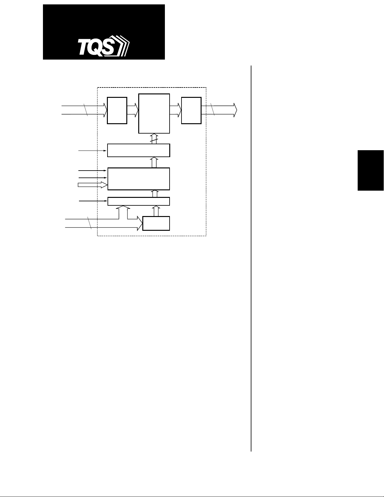
34 x 34
Crosspoint
Switch Matrix
6:34 Decoder
Output
Buffers
TQ8034
OUT0:33
68
IN0:33
CONFIGURE
LOAD
MODE(1)
IADD0:5
MODE(0)
OADD0:33
Input
Buffers
68
34 6-Bit Configuration Latches
34 6-Bit Program Latches
Output Address Select
0:33
34
The TQ8034 is a non-blocking 34 X 34 digital crosspoint switch capable of data
rates greater than 1.6 Gigabits per second per port. Utilizing a fully differential
data path from input to output, the TQ8034 offers a high data rate with
exceptional fidelity. The symmetrical switching and noise rejection
characteristics inherent in differential logic result in low jitter, low crosstalk and
minimum signal skew. The TQ8034 is ideally suited for gigabit data and HDTV
switching applications.
1.6 Gbit/sec
3.3V 34x34 Digital
Crosspoint Switch
Features
• >1.6 Gb/s port data bandwidth
>50 Gb/s aggregate bandwidth
• 3.3V power supply
• Fully differential data path for
superior signal fidelity
• Non-blocking architecture
• Full broadcast and multi-cast
capability
• Differential LVPECL I/O with
TTL control
• On-chip 50 Ohm LVPECL input
termination
• Low jitter and signal skew
• Two-stage configuration register
• Multiple programming modes
PRODUCTS
SWITCHING
The non-blocking architecture uses 34 fully independent 34:1 multiplexers,
allowing each output port to be independently programmed to any input port.
The TQ8034 supports full broadcast and multicast operation, with
programming modes optimized for these applications.
Four methods are provided for configuration of the switch. Two modes are
used for programming one input to one output at a time and the other two are
for programming one input to multiple outputs (1 to 34) at once. In all modes,
data integrity is maintained on all unchanged data paths.
For additional information and latest specifications, see our website: www.triquint.com
• 304-pin BGA package
Applications
• Telecom/datacom switching
including Fibre Channel and
Gigabit Ethernet
• Hubs and routers
• Video switching including
High-Definition TV (HDTV)
1

TQ8034
PRELIMINARY DATA SHEET
Circuit Description
Data inputs
The 34 input channels are differential LVPECL
compatible with on-chip 50-Ohm termination to VTT.
Unused input-pairs should have one side connected to
GND through a 500-Ohm or smaller resistor to prevent
unwanted oscillations. See figure 6 for examples of DC
and AC coupled termination.
Data outputs
The 34 output channels are differential LVPECL
compatible and designed to be terminated through 50Ohms to VDD-2.0V. Unused outputs can be left unterminated to save power. See figure 6 for examples of
DC and AC coupled termination.
Control Inputs
The control inputs are TTL compatible. Unconnected
inputs will default to logic HI levels.
Configuration Storage
Each of the 34 output channels has two sets of
configuration storage registers. The registers are built
using transparent latches which are controlled by the
LOAD and CONFIGURE inputs. The first set of latches,
or program register, stores a new input configuration
prior to application to the switch core. The second set
of latches, or configuration register, stores the
configuration that is applied to the switch core. The
use of two sets of program storage latches allows new
configurations to be loaded without disturbing the
existing configuration. The two-stage architecture also
allows all of the new configurations to be applied to the
switch core simultaneously.
Configuration Modes
There are two primary modes for configuring the
TQ8034; Sequential and Multicast. Sequential mode is
used to program one input to one output per LOAD
cycle and Multicast is used to program one input to
multiple outputs per LOAD cycle. Both modes allow
either a user defined input port assignment or an
internal default input port assignment.
The default input port assignment for each output port
is the output's corresponding input port (IN0 to OUT0,
IN1 to OUT1, etc.). This default configuration is
referred to as pass-through.
All programming modes result in the loading of a new
configuration into the appropriate output port
PROGRAM (first stage) registers. Changing the
contents of the PROGRAM registers does not change
the configuration of the switch core. The configuration
of the switch core is updated following the assertion of
CONFIGURE. CONFIGURE is a global input that
simultaneously transfers the contents of all PROGRAM
registers into their second stage CONFIGURATION
registers. The data is latched into the CONFIGURATION
register when CONFIGURE is de-asserted.
The integrity of the data flowing through the switch
core is maintained during the load cycle. The integrity
of the data flowing through the switch core to outputs
that do not receive a new configuration is also
maintained during the configure cycle. Data integrity is
unknown on output ports receiving a new input port
configuration for a time
Tdcf
after assertion of
CONFIGURE (see timing diagrams).
The CONFIGURE inputs can be tied to a "HI" level or
asserted simultaneously with LOAD. In this case, the
new configuration will be applied to the switch
multiplexer when LOAD is asserted.
2
For additional information and latest specifications, see our website: www.triquint.com

TQ8034
PRELIMINARY DATA SHEET
The configuration modes are defined by the MODE0
and MODE1 control inputs.
MODE0 MODE1 Switch Configuration Mode
0 0 Sequential Mode: User defined input port assignment
0 1 Sequential Mode: Default input port assignment
1 0 Multicast Mode: User defined input port assignment
1 1 Multicast Mode: Default input port assignment
Sequential Program Mode
Sequential programming allows for a single input to
output port assignment per LOAD cycle. Any number
of port assignments can be made with repeated LOAD
cycles prior to assertion of CONFIGURE.
User defined input port assignment
(MODE0=0, MODE1=0)
User defined input port assignment Sequential
programming uses the address inputs IADD(0:5) and
the lower 6 bits of OADD(0:33).
To program, apply the desired output port address to
the address inputs OADD(0:5) and the desired input
port address to the address inputs IADD(0:5). The
input address defines which input port connects to the
selected output port. The new configuration is loaded
into the PROGRAM register by asserting the LOAD
input high and is latched when LOAD is de-asserted.
Default input port assignment (MODE0=0, MODE1=1)
Default input port assignment Sequential programming
uses the same lower 6 bits of OADD(0:33) and ignores
the IADD(0:5) inputs.
configuration is loaded into the PROGRAM register by
asserting the LOAD input high and is latched when
LOAD is de-asserted.
Multicast Program Mode
Multicast programming allows any combination of
output ports to be configured to a single input port in a
single LOAD cycle.
User defined input port assignment
(MODE0=1, MODE1=0)
User defined input port assignment Multicast
programming uses input addresses IADD(0:5) and
output addresses OADD(0:33).
To program, apply the desired input port address to
IADD(0:5) and the OADD(0:33) bits which correspond
to the desired output ports. For example, to program
input 1 to output ports 1, 2 and 5; apply "000001" to
IADD(0:5) and apply "00..0100110" to OADD(0:33). The
new configuration is loaded into the program latches
by asserting the LOAD signal high and is latched when
LOAD is de-asserted. This process is continued for
each set of outputs to be programmed to a unique
input. Data is then transferred to the CONFIGURATION
latches upon assertion of CONFIGURE input.
Default input port assignment (MODE0=1, MODE1=1)
Default input port assignment Multicast programming
uses the OADD(0:33) inputs and ignores the IADD(05)
inputs. Apply the desired output ports to be configured
to inputs OADD(0:33). Upon assertion of LOAD, each
output port selected will be programed to its
corresponding input port.
PRODUCTS
SWITCHING
To program, apply the desired output port address to
the address inputs OADD(0:5). The default
For additional information and latest specifications, see our website: www.triquint.com
3

TQ8034
PRELIMINARY DATA SHEET
Specifications
Specifications subject to change without notice
Table 1. Absolute Maximum Ratings
4
Parameter Condition Symbol Minimum Nominal Maximum Unit
Storage Temperature T
Junction Temperature T
Case Temperature w/bias (1) T
Supply Voltage (2) V
Voltage to any input (2) V
Voltage to any output (2) V
Current to any TTL input (2) I
Current from any output (2) I
Power Dissipation of output (3) P
store
CH
C
DD
in
out
in
out
out
–65 150 °C
–65 150 °C
0 100 °C
0 5.5 V
–0.5 VDD + 0.5 V
–0.5 V
+ 0.5 V
DD
–1.0 1.0 mA
40.0 mA
50.0 mW
Electrostatic Discharge ESD 2000 V
Notes: 1. Tc is measured at case top.
2. All voltages are measured with respect to GND (0V) and are continuous.
– V
) x I
3. Pout = (V
4. Absolute maximum ratings, as detailed in this table, are the ratings beyond which the device’s performance may be impaired
and/or permanent damage to the device may occur.
DD
out
Table 2. Recommended Operating Conditions
out
.
7
Symbol Parameter Min Typ Max Units Notes
T
C
Case Operating Temperature 0 — 100 °C1
VDDSupply Voltage 3.14 — 3.47 V
I
DDcore
I
DDoutput
V
TT
R
LOAD
P
Dcore
P
Doutput
P
DinputAC
P
DinputDC
Θ
JC
Notes: 1. TC measured at case top. Use of adequate heatsink is required.
4
Positive Supply Current Switch Core 2.25 A
Positive Supply Current Per Output Pair 30 mA 2
Load Termination Supply Voltage VDD – 2.0 V 3
Output Termination Load Resistance 50 Ω 3
Power Dissipation Switch Core 7.4 W
Dissipation per terminated output pair 32 mW 4
Dissipation per AC coupled input pair 2.8 mW 5
Dissipation per DC coupled input pair 9.8 mW 6
Thermal Resistance Junction to Case 2.2 °C/W
2. I
3. The V
4. PDoutput is additive to P
5. P
6. P
7. Functionality and/or adherence to electrical specifications is not implied when the device is subjected to conditions that exceed,
is additive to I
DDoutput
and R
TT
is additive to P
DinputAC
is additive to P
DinputDC
singularly or in combination, the operating range specified.
For additional information and latest specifications, see our website: www.triquint.com
combination is subject to maximum output current and power restrictions.
LOAD
for each terminated differential output pair (true and complement).
DDcore
for each terminated differential output pair (true and complement).
Dcore
for each AC-coupled differential input pair (true and complement).
Dcore
for each DC-coupled differential input pair (true and complement).
Dcore
TQ8034
PRELIMINARY DATA SHEET
Table 3. DC Characteristics—PECL I/O
3
Parameter Condition Symbol Minimum Nominal Maximum Unit
Input common mode voltage range V
Input differential voltage (pk-pk) (1) V
Output common mode voltage range V
Output differential voltage (pk-pk) (2) V
Input termination resistance R
Table 4. DC Characteristics—TTL Inputs
3
ICOM
IDIFF
OCOM
ODIFF
IN
VDD – 1500 — VDD – 1100 mV
600 — 2400 mV
VDD-1500 — VDD – 1100 mV
1200 — 2400 mV
50 Ohm
Parameter Condition Symbol Minimum Nominal Maximum Unit
Input HIGH voltage V
Input LOW voltage V
Input HIGH current V
Input LOW current V
IH(MAX)
IL(MIN)
Input capacitance C
Notes (Tables 3 and 4):
1. Differential inputs.
2. R
= 50 ohms to VTT = VDD – 2.0V.
LOAD
3. Specifications apply over recommended operating ranges.
IH
IL
I
IH
I
IL
IN
2.0 — VDD+1.8 V
0 — 0.8 V
— — 200 uA
–400 –200 — uA
— — TBD pF
PRODUCTS
SWITCHING
For additional information and latest specifications, see our website: www.triquint.com
5
 Loading...