

TriQuint Semiconductor Inc TQ8033 Datasheet
T R I Q U I N T S E M I C O N D U C T O R , I N C .
TQ8033
DATA SHEET
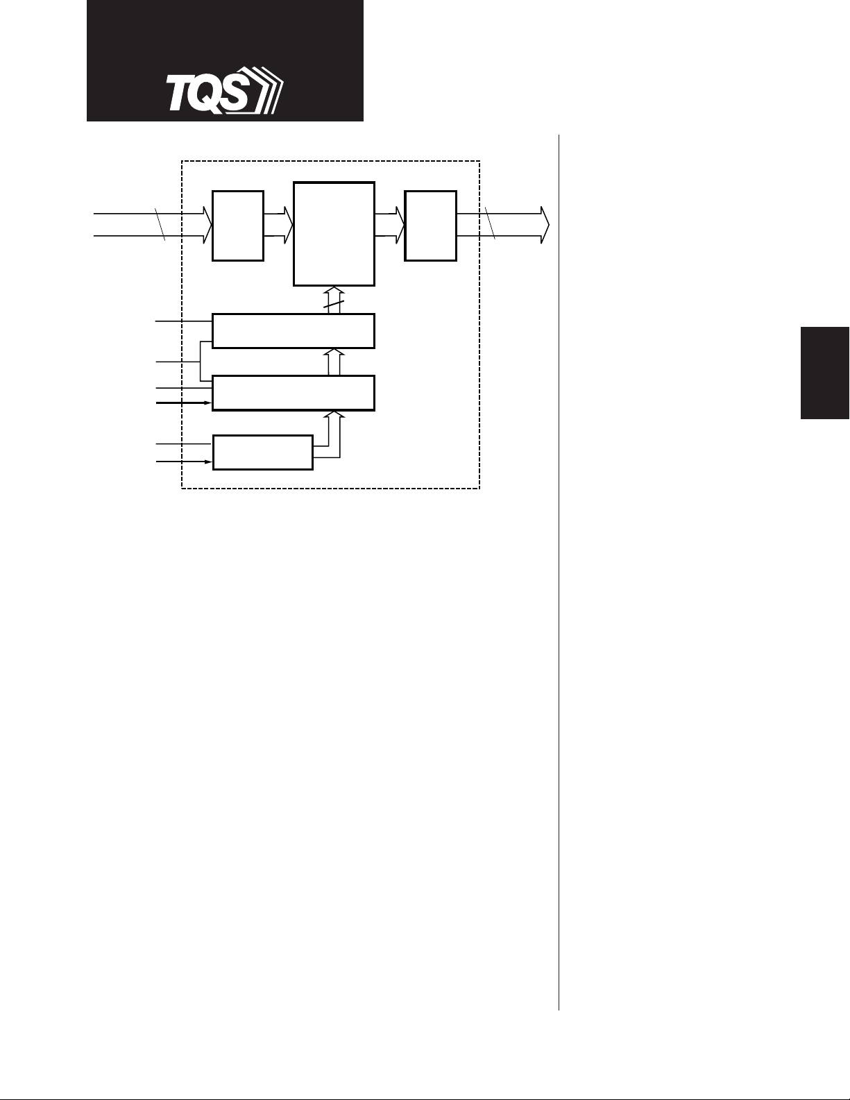
64 x 33
Crosspoint
Switch Matrix
Output
Buffers
TQ8033
O0–O32
66
D0–D63
CONFIGURE
RESETIN
LOAD
IADD(0:5)
MONITOR_LD
O
ADD(0:4)
Input
Buffers
128
33 6-Bit Configuration Latches
33 6-Bit Program Latches
5:32 Decoder
The TQ8033 is a non-blocking 64 x 33 digital crosspoint switch that
supports data rates greater than 1.5 gigabits per second per channel.
The TQ8033's non-blocking architecture allows any combination of
output-to-input programming, supporting both broadcast and multicast
applications. Using 33 independent 64:1 multiplexers, each output
channel can be programmed to any input without restriction or
degradation of signal fidelity.
1.5 Gbit/sec
64x33 Expandable
Crosspoint Switch
Features
• >1.5 Gb/s/port data rate
>50 Gb/s aggregate bandwidth
• Differential PECL data path with
64 inputs and 33 outputs
• Non-blocking architecture
supports Broadcast and
Multicast operation
• Data inputs internally biased for
AC coupling
• Low jitter and signal skew
• Double-buffered configuration
latches
• TTL configuration control inputs
PRODUCTS
SWITCHING
The TQ8033's architecture is ideally suited for building larger switch
arrays. By eliminating the need to "wire-or" or buss the outputs to
interconnect multiple devices, the maximum system bandwidth and signal
fidelity is achived.
Designed for use in high-performance / high-capacity switching
applications, the TQ8033 data path is fully differential to minimize jitter,
skew, and signal distortion. The data path interface levels are PECL and
the configuration and control interface levels are TTL.
The TQ8033 is the ideal switching solution for HDTV digital video, data
communications (Fibre Channel and Gigabit Ethernet) and
telecommunications applications.
For additional information and latest specifications, see our website: www.triquint.com
• 304-pin BGA package
• Single +5V supply
Applications
• Telecom/datacom switching
including Fibre Channel and
Gigabit Ethernet
• Hubs and routers
• Video switching including
High-Definition TV (HDTV)
1

TQ8033
DATA SHEET
Circuit Description
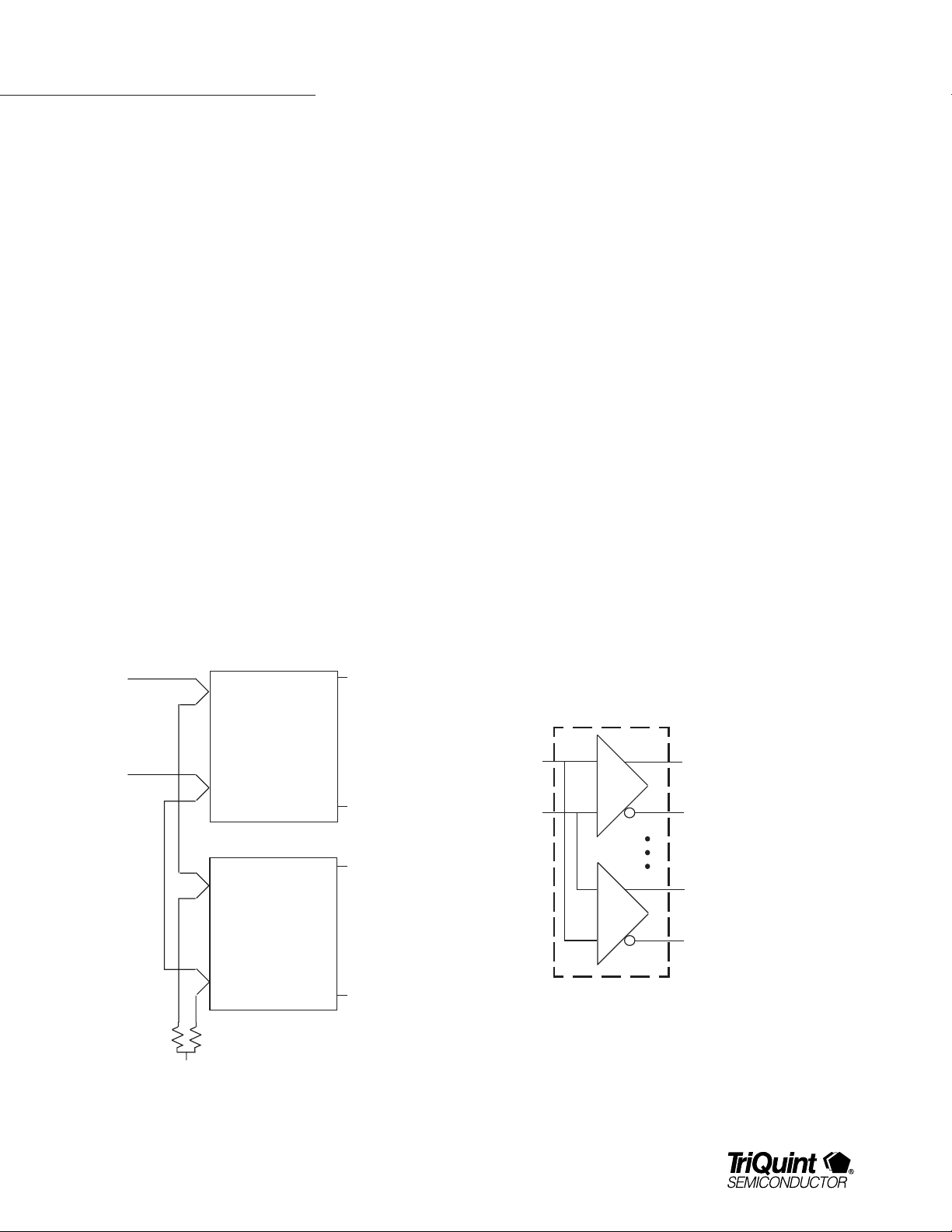
Data Inputs
The 64 data input channels are differential PECL
compatible. All inputs have a 2.5KΩ Thevenin
equivalent bias circuit which holds the DC bias at
-1.3 Volts simplifying the design of applications
V
DD
requiring AC coupling. Input signals must be properly
terminated for maximum performance. Terminate one
side (true or complement) of any unused inputs to V
Data Outputs
The 33 data output channels are differential PECL
compatible and designed to be terminated to 50Ω to
-2.0 Volts. Unused outputs can be left
V
DD
unterminated if desired in order to save power.
Control Inputs
To program the TQ8033, the address of the desired
output port is applied to the inputs (OADD0:4; where
00000=O0 and 11111=O31). The address of the desired
input port is applied to the inputs (IADD0:5; where
000000=I0 and 111111=I63).
The new configuration is loaded into the program
registers by asserting the LOAD signal high. The data
is latched when LOAD is de-asserted. LOAD should
.
remain low and only be asserted for the time necessary
TT
to load the new configuration data.
The process is repeated for each output port
configuration. Only the output ports which are to
receive a new input port configuration need to be
programmed. The new configurations are not applied
to the switch core at this time and there is no
disruption of the data flowing through the switch core.
The control inputs interface levels are TTL compatible.
Program Registers
The configuration data for each of the 33 data channels
have two sets, or stages, of configuration storage
registers. The first stage, known as the program
register, stores a new set of input configurations prior
to application to the switch core. The second stage,
known as the configuration register, stores the current
switch core configurations.
The use of two stage configuration storage registers
allows new input configurations to be loaded without
disturbing the existing configuration. After the new
input configurations have been loaded into the program
registers, the CONFIGURE input is asserted and the
new configurations are applied to the switch core.
After the new configurations have been loaded into the
program registers, the CONFIGURE input is asserted
and the data in the program registers is loaded into the
configuration registers. The data is latched on the
falling edge of CONFIGURE.
The switch core receives the new configuration as soon
as CONFIGURE is asserted. During the time the new
configurations are being applied to the switch core, the
integrity of the data on output ports which receive a
tdcf
new configuration is unknown for a period of
from
the time CONFIGURE is asserted.
If desired, the LOAD and CONFIGURE can be asserted
simultaneously. In this mode, the new configuration
will be applied to the switch core when LOAD is
asserted.
2
For additional information and latest specifications, see our website: www.triquint.com

TQ8033
DATA SHEET
Programming the Monitor Port
The 33rd output port, called the monitor port, is
programmed in the same manner as the other 32
output ports with the exceptions that the LOAD and
Output Address inputs are ignored.
To program the monitor port, apply the desired input
port address to inputs (IADD0:5) and assert the
MONITOR_LD input. Like the other 32 output ports, the
CONFIGURE input is asserted to apply the new
configuration to the switch core.
Reset Programming
The RESETIN is an active high input which sets all of
the switch multiplexers to a defined configuration.
There are three RESET modes available when RESETIN
is used in conjunction with CONFIGURE and IADD5
inputs.
The monitor port is reset to input D0 regardless of the
state of CONFIGURE or IADD5.
Mode 1 is broadcast operation. In this mode, the
RESETIN signal clears all of the configuration registers
immediately forcing all output ports to be connected to
input port 0. The device will remain in the Mode 1 reset
state as long as the RESETIN input is asserted.
Modes 2 and 3 place the device into pass-through
configuration. The mode is controlled by the assertion
of CONFIGURE immediately following the de-assertion
of RESETIN and the state of input IADD5.
Mode 2, or low-order pass-through, is set with the
assertion of CONFIGURE with IADD5 input low. In this
mode, inputs D0 to D31 are configured to outputs O0
to O31 respectively (D0 to O0, D1 to O1,,,D31 to O31).
Mode 3, or high-order pass-through, is set with the
assertion of CONFIGURE with IADD5 input high. In this
mode, inputs D32 to D63 are configured to outputs O0
to O31 respectively (D32 to O0, D33 to O1,,,D63 to
O31).
PRODUCTS
SWITCHING
Reset Configuration Modes
Mode RESETIN CONFIGURE** IADD5** RESET Configuration
1 1 0 X Broadcast mode. All outputs programmed to input 0
2 1 1 0 Low-order Pass-through mode #1.
3 1 1 1 High-order Pass-through mode #2.
** Valid only when asserted immediately following de-assertion of RESETIN and prior to any new program cycles.
For additional information and latest specifications, see our website: www.triquint.com
3
TQ8033
DATA SHEET
Building Switch Arrays with the TQ8033
By eliminating the need to “wire-or” the outputs of
multiple devices or to add additional switch elements to
get the necessary routing channels, the TQ8033 offers
the highest performance solution with the least number
of devices for implementing larger array sizes.
The 33rd output port provides an additional data
channel for system data links or for diagnostics system
monitoring of each switch element within the array. The
following examples show how to interconnect multiple
TQ8033 devices to create a 64x64 and a 128x128
switch array.
64x64 Switch Array
To implement a 64x64 array
(figure 2)
, only two
TQ8033 devices are required and the data passes
through only one switch element. For applications with
data rates less than one gigabit per second, a technique
known as"fly-by" termination offers good signal fidelity
with the minimum number of components. To
implemement, both the input signal pairs (true and
complement) are routed to both devices and then to the
termination network at the end of the signal trace with
the minimum number of trace discontinuities.
To accomplish this, route the trace from the source
device to the first TQ8033 input pad and then continue
the signal trace from the input pads to the next device,
and finally to the termination network.
For applications at data rates above one gigabit per
second, it is recommended to use a fan-out buffer to
drive each TQ8033 input as shown in
figure 3
.
As with any high speed interconnect, careful attention
to the impedance of the signal traces is very important.
D0
O0
TQ8033
D63
O31
O32
TQ8033
O63
50
50
Ω
V
Figure 2. 64x64 array with "fly-by" termination
Ω
TT
Dn/
NDn
Connect one driver
output to each
common TQ8033
input
Figure 3. Optional fan-out buffer for array expansion
4
For additional information and latest specifications, see our website: www.triquint.com
TQ8033
DATA SHEET
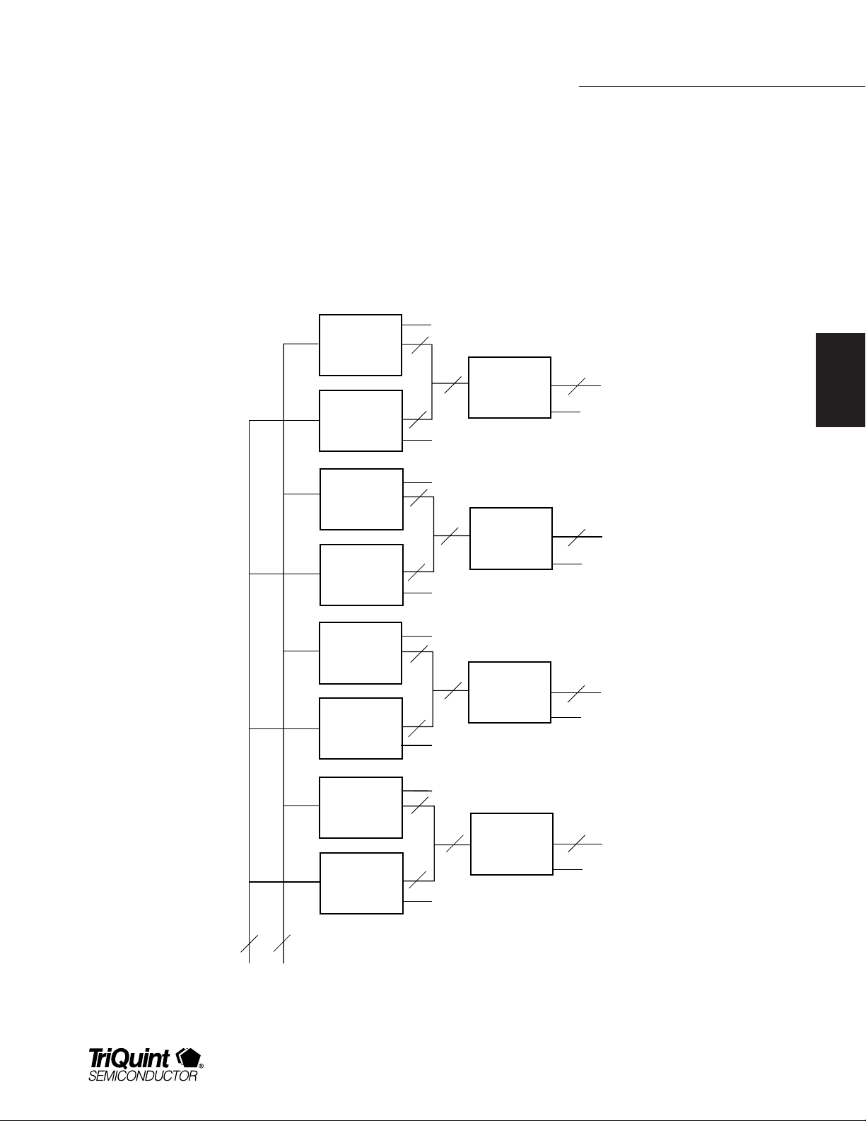
128x128 Switch Array
To implement a 128x128 switch array, simply extend
the design of the 64x64 switch array to include the
additional devices. In this configuration, only 12
TQ8033 devices are required and the signal passes
through only two switch stages.
TQ8033
64x33
Crosspoint
Switch
TQ8033
64x33
Crosspoint
Switch
TQ8033
64x33
Crosspoint
Switch
TQ8033
64x33
Crosspoint
Switch
Monitor
Monitor
Monitor
Monitor
Again, use “fly-by” interconnection or a fan-out buffer on
input signals to connect multiple devices and the far-end
termination network.
Larger switch arrays can be built by simply adding
additional TQ8033 devices.
32
64
32
32
64
32
TQ8033
64x33
Crosspoint
Switch
TQ8033
64x33
Crosspoint
Switch
32
Monitor
32
Monitor
D0-31
D32-63
PRODUCTS
SWITCHING
D0-63
6464
D64-127
TQ8033
64x33
Crosspoint
Switch
TQ8033
64x33
Crosspoint
Switch
TQ8033
64x33
Crosspoint
Switch
TQ8033
64x33
Crosspoint
Switch
Monitor
32
32
Monitor
Monitor
32
32
Monitor
64
64
Figure 4. 128x128 array
TQ8033
64x33
Crosspoint
Switch
TQ8033
64x33
Crosspoint
Switch
32
D64-95
Monitor
32
D96-127
Monitor
For additional information and latest specifications, see our website: www.triquint.com
5
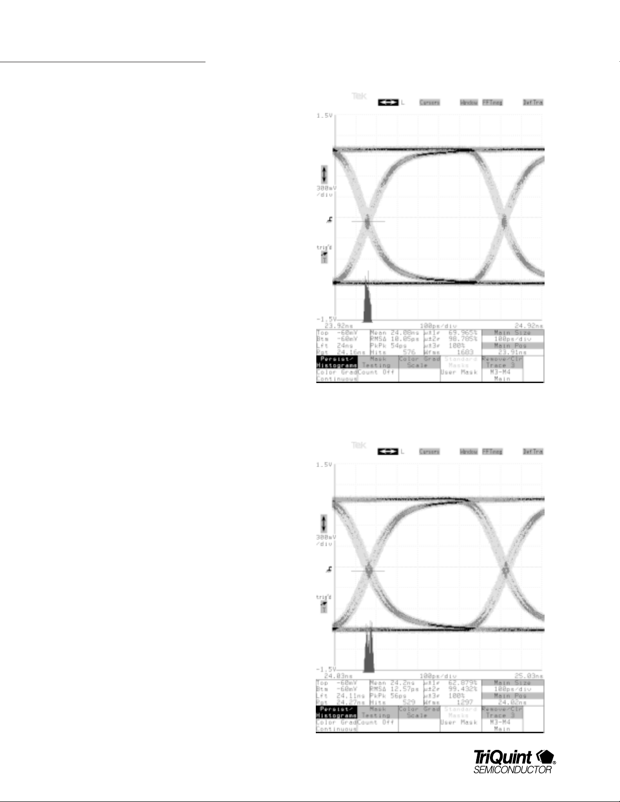
Typical Performance
Data Rate: 1.5Gb/s
Data Pattern: 2
Case Temperature: 0° C
Jitter: 54 ps pk-pk
TQ8033
DATA SHEET
23-1
PRBS
Data Rate: 1.5Gb/s
23-1
Data Pattern: 2
PRBS
Case Temperature: 85° C
Jitter: 56 ps pk-pk
6
For additional information and latest specifications, see our website: www.triquint.com
 Loading...