

TriQuint Semiconductor Inc TQ8032-M Datasheet
T R I Q U I N T S E M I C O N D U C T O R , I N C .
SWITCHING
PRODUCTS
1
For additional information and latest specifications, see our website: www.triquint.com
Min Max Units
Data Rate/Port 800 Mb/s
Jitter 150 ps pk-pk
Channel Propagation Delay 2300 ps
Ch-to-Ch Propagation Delay Skew 500 ps
Input
Buffers
Output
Buffers
32 x 32
Crosspoint
Switch
Matrix
32 5-Bit
Configuration Latches
32 5-Bit
Program Latches
5
5
5:32
Decoder
O0 – 31D0 – 31
CONFIGURE
RESET
LOAD
CNTRL LVL
IA0 – 4
OA0 – 4
TQ8032
64
64
TQ8032
800 Megabit/sec
32x32 Digital ECL
Crosspoint Switch
Applications
•
Telecom/Datacom Switching
•
Hubs and Routers
•
Video Switching
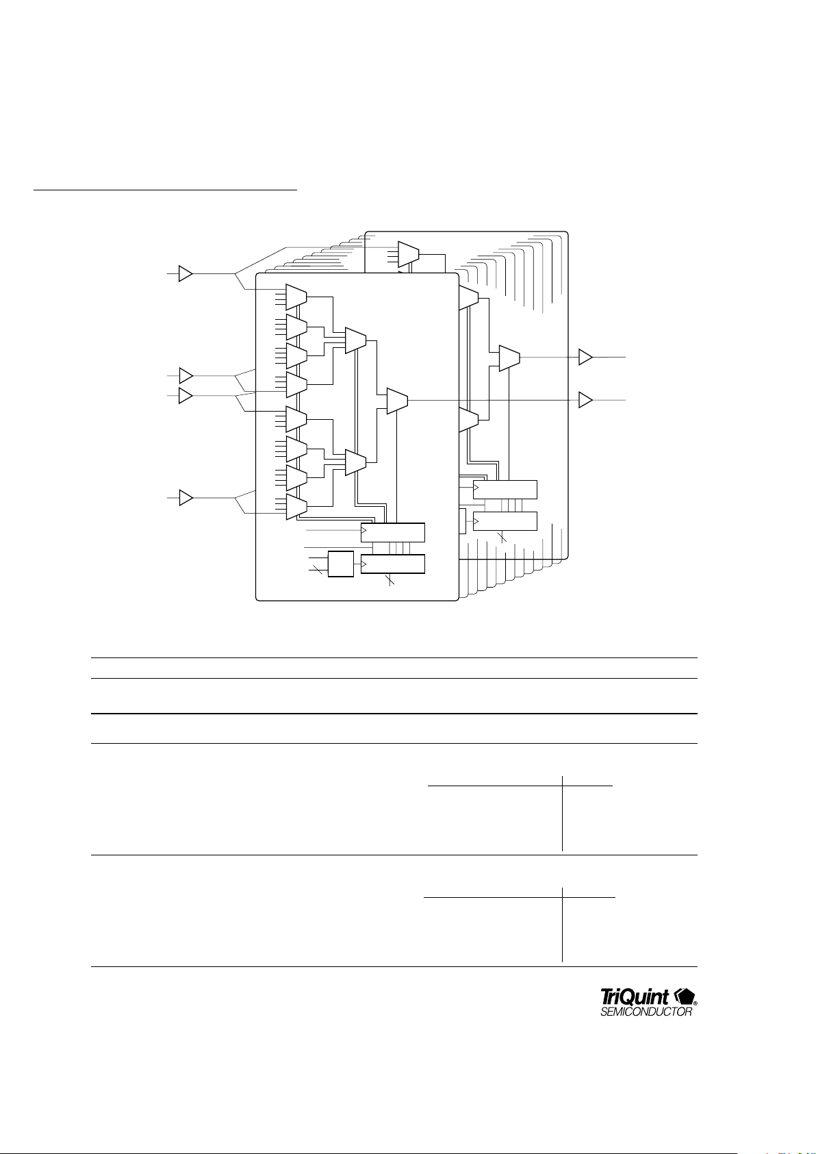
The TQ8032 is a non-blocking 32 x 32 digital crosspoint switch capable of
800 Megabits per second per port data rates. Utilizing a fully differential
internal data path and ECL I/O, the TQ8032 offers a high data rate with
exceptional signal fidelity. The symmetrical switching and noise rejection
characteristics inherent in differential logic result in low jitter and signal
skew. The TQ8032 is ideally suited for digital video, data communications
and telecommunication switching applications.
The non-blocking architecture uses 32 fully independent 32:1 multiplexers
(see diagram on page 2), allowing each output port to be independently
programmed to any input port. The switch is configured by sequentially
loading each multiplexer’s 5-bit program latch (OA0:4) with the desired
input port address (IA0:4) and enabling the LOAD pin. When complete, the
CONFIGURE pin is strobed and all new configurations are simultaneously
transferred into the switch multiplexers. Data integrity is maintained on all
unchanged data paths.
Features
•
>25 Gb/s aggregate BW
•
800 Mb/s/port NRZ data rate
•
Non-blocking architecture
•
500 ps delay match
•
Differential ECL-level data
I/O; Selectable CMOS/TTLlevel control inputs
•
Low jitter and signal skew
•
Fully differential data path
•
Double buffered configuration
latches
•
196-pin CQFP package
Electrical Characteristics
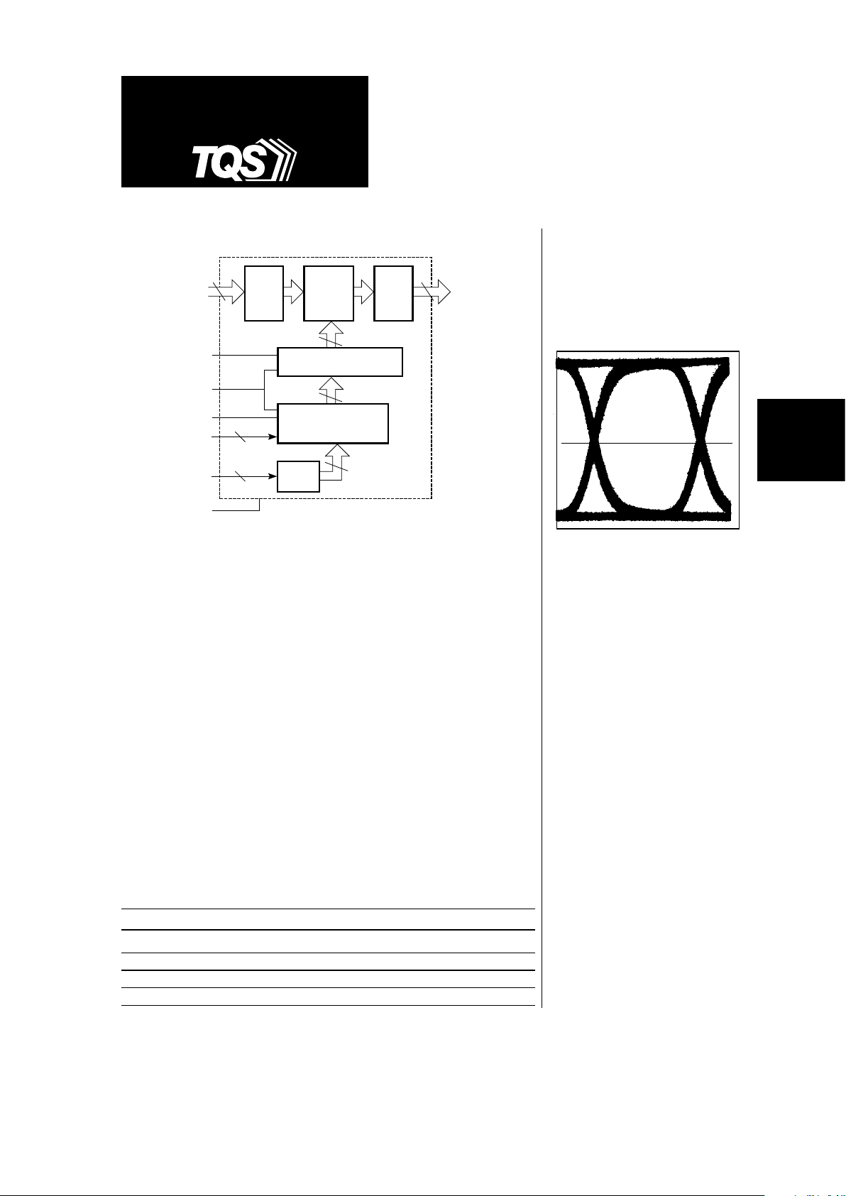
Typical output waveform with all
channels driven
TQ8032
For additional information and latest specifications, see our website: www.triquint.com
2
Signal Name/Level Description
I0 to I31, Data input true and complement. Differential data input ports.
NI0 to NI31 Differential ECL
O0 to O31, Data output true and complement. Differential data output ports.
NO0 to NO31 Differential ECL
IA0:4 Input address. CMOS/TTL Input port selection address that is written into the selected output port
program latches (OA0:4).
IA4 IA3 IA2 IA1 IA0 Input port
00000 0
00001 1
00010 2
::::: :
11111 31
OA0:4 Output select address. Output port selection address. Selects the output port program latches to
CMOS/TTL which the input port selection address (IA0:4) is written.
OA4 OA3 OA2 OA1 OA0 Output port
00000 0
00001 1
00010 2
::::: :
11111 31
Table 2. Pin Descriptions
Figure 1. Architecture
DATA
OUT 31
(O31)
5
RESET
OUTPUT
SELECT ADDRESS
(OA0:4)
Input
Buffers
DATA
OUT 0
(O0)
.
.
.
.
.
.
.
.
.
.
.
.
.
.
.
.
Output
Buffers
Configuration
Register
Program Register
CONFIGURE
LOAD
5
32 X 1-BIT
MULTIPLEXER
DATA IN 0
(I0)
DATA IN 15
(I15)
Input
Buffers
.
.
.
.
.
.
.
.
.
.
.
.
DATA IN 16
(I16)
DATA IN 31
(I31)
5
INPUT ADDRESS
(IA0:4)
5:32
DECODE
32 X 1-BIT
MULTIPLEXER
TQ8032
SWITCHING
PRODUCTS
3
For additional information and latest specifications, see our website: www.triquint.com
VEE (-5V)
NI7
I7
GND
NI6I6NI5
I5
GND
NI4I4NI3
I3
GND
NI2I2NI1
I1
GND
NI0
I0
RESET
GND
O0
NO0
GND
O1
NO1O2NO2
GND
O3
NO3O4NO4
GND
O5
NO5O6NO6
GND
O7
NO7
CTRL LVL
VCC (+5V)
12345678910111213141516171819202122232425262728293031323334353637383940414243444546474849
147
146
145
144
143
142
141
140
139
138
137
136
135
134
133
132
131
130
129
128
127
126
125
124
123
122
121
120
119
118
117
116
115
114
113
112
111
110
109
108
107
106
105
104
103
102
101
100
99
VCC (+5V)
GND
I27
NI27
I28
NI28
GND
I29
NI29
I30
NI30
GND
I31
NI31
IA(4)
IA(3)
GND
IA(2)
IA(1)
IA(0)
CONFIG
GND
LOAD
OA(4)
OA(3)
OA(2)
GND
OA(1)
OA(0)
NO31
O31
GND
NO30
O30
NO29
O29
GND
NO28
O28
NO27
O27
GND
NO26
O26
VEE (-5V)
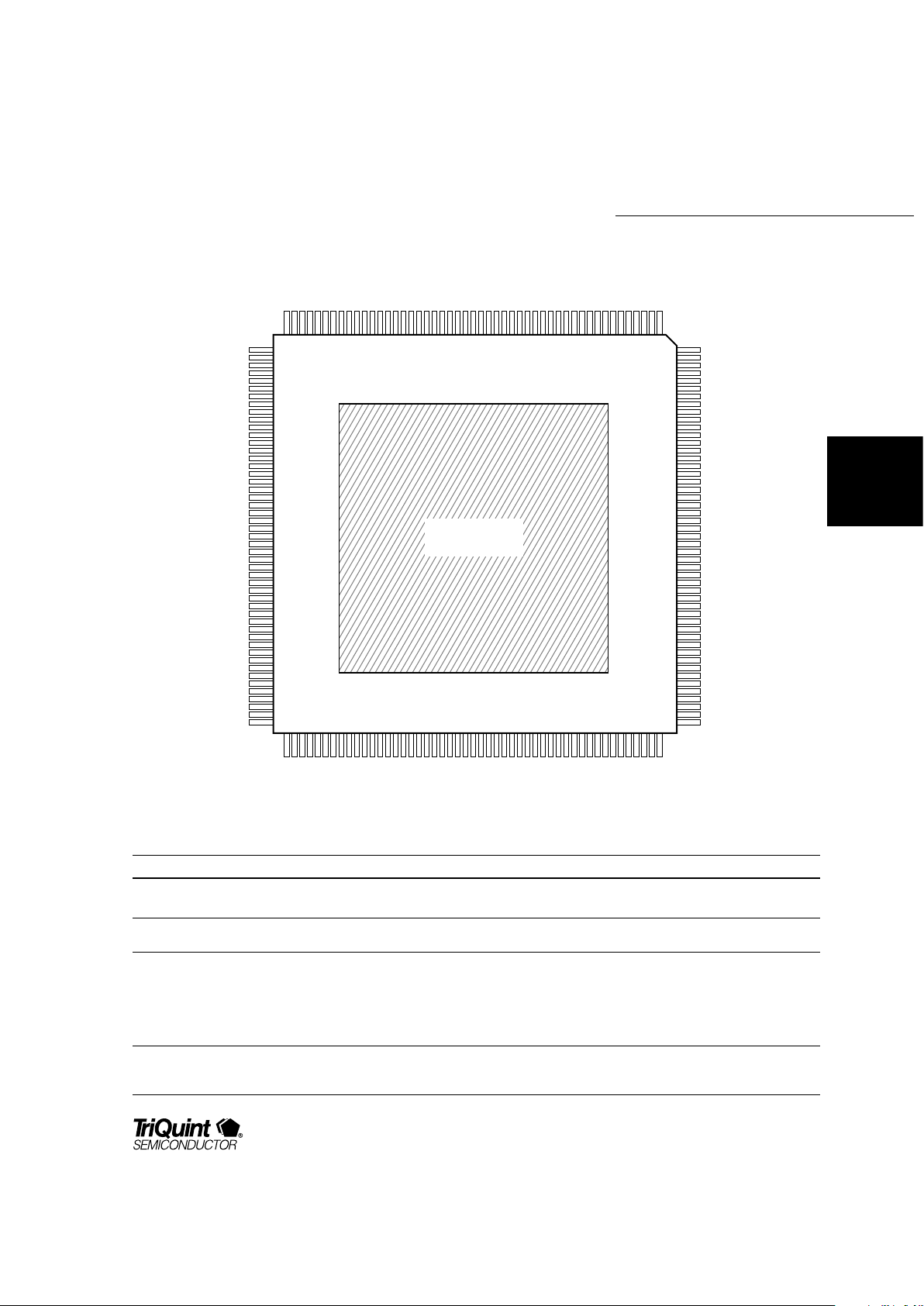
Top View
196-Pin Package
NOTE: All unmarked pins are not connected.
196
195
194
193
192
191
190
189
188
187
186
185
184
183
182
181
180
179
178
177
176
175
174
173
172
171
170
169
168
167
166
165
164
163
162
161
160
159
158
157
156
155
154
153
152
151
150
149
148
VEE (-5V)
I8
NI8
I9
GND
NI9
I10
NI10
I11
GND
NI11
I12
NI12
I13
GND
NI13
I14
NI14
I15
GND
NI15
I16
NI16
I17
GND
NI17
I18
NI18
I19
GND
NI19
I20
NI20
I21
GND
NI21
I22
NI22
I23
GND
NI23
I24
NI24
I25
GND
NI25
I26
NI26
VCC (+5V)
50
51
52
53
54
55
56
57
58
59
60
61
62
63
64
65
66
67
68
69
70
71
72
73
74
75
76
77
78
79
80
81
82
83
84
85
86
87
88
89
90
91
92
93
94
95
06
97
98
VCC (+5V)
O8
NO8
GND
O9
NO9
O10
NO10
GND
O11
NO11
O12
NO12
GND
O13
NO13
O14
NO14
GND
O15
NO15
O16
NO16
GND
O17
NO17
O18
NO18
GND
O19
NO19
O20
NO20
GND
O21
NO21
O22
NO22
GND
O23
NO23
O24
NO24
GND
O25
NO25
VEE (-5V)
Signal Name/Level Description
LOAD CMOS/TTL Enables the selected output port program latches while set ‘high’.
Latches the data when set to a 'low' level.
CONFIGURE CMOS/TTL Transfers the program latches data to the configuration latches and implements
the switch changes while set "high." Latches the data when set to a "low" level.
RESET CMOS/TTL Puts the switch into
Broadcast
or
Pass-Through
configuration, overwriting
existing configurations.
Broadcast mode: All output ports are connected to data input port 0. This mode
is selected by applying a RESET “high” pulse with CONFIGURE held “low."
Pass-through mode: I0 is connected to O0, I1 to O1, etc. This mode is selected
by applying a RESET “high” pulse with CONFIGURE held “high."
CNTRL LVL Input level control. GND/Open Selects the input levels for the input address (IA0:4), output address(OA0:4),
CONFIGURE, LOAD and RESET inputs. Inputs are configured for TTL when
tied to GND and CMOS when left unconnected.
Table 2. Pin Descriptions (continued)
Figure 2. Package Pinout
 Loading...