

TriQuint Semiconductor Inc TQ8025 Datasheet
T R I Q U I N T S E M I C O N D U C T O R , I N C .
TQ8025
PRELIMINARY DATA SHEET
2.5 Gigabit/sec
DIØ–15
(differential)
32
PECL/CML
Input
Buffers
16 x 16
Crosspoint
Switch Matrix
PECL/CML
Output
Buffers
32
DOØ–15
(differential)
Configuration
Latches
4-Bit Shift
Register
4-Bit Shift
Register
16 x 4
Address Generator
and Control
READY
+5V
GND
RADDØ
RADD1
RESET–
LDMODE
CONFIG
ADD15
ADDØ
LOAD
CLOCK
ADDREN
AUTOCONFIG
TQ8025
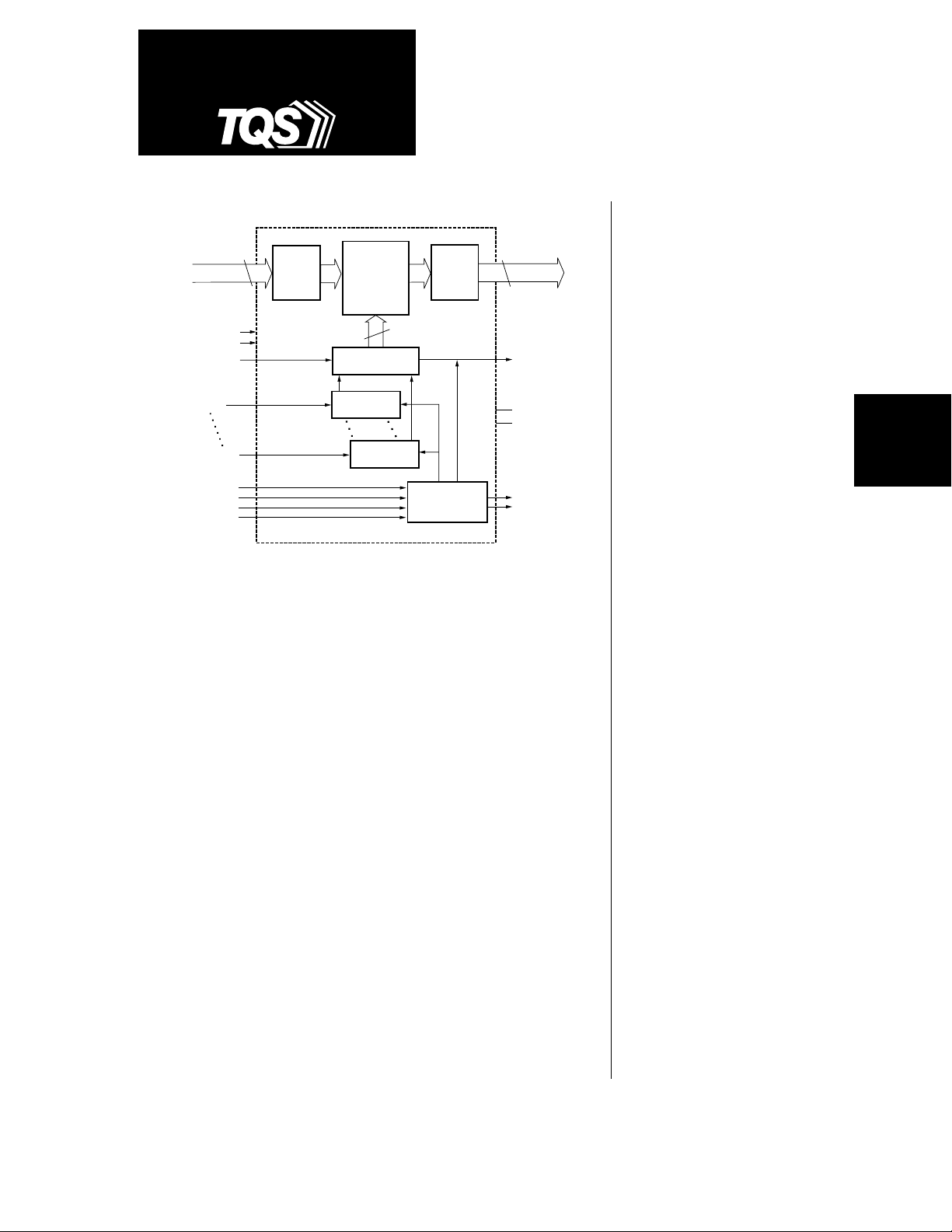
The TQ8025 is a non-blocking 16 x 16 digital crosspoint switch capable of
data rates greater than 2.5 gigabits per second per port. With a fully
differential internal data path and PECL/CML I/O, the TQ8025 offers an
extremely high data rate with exceptional signal fidelity. The use of fully
differential logic results in low crosstalk, jitter, and signal skew. The
TQ8025 is ideally suited for digital video, data communications,
telecommunication switching, and cross-connect applications.
The non-blocking architecture uses 16 fully independent 16:1 multiplexers
which allow each output port to be independently programmed to any input
port. The TQ8025 offers two programming options: a flexible port-by-port
option, and a fast configuration option.
16x16 Digital
Crosspoint Switch
Features
• 16 PECL/CML fully differential
(back-terminated) outputs
• >2.5 Gb/s data bandwidth
per channel
• >40 Gb/s aggregate bandwidth
• Non-blocking architecture
• 80 ns configuration time
• Autonomous control of external
RAM for configuration data
• Low jitter and signal skew
•
±
100 ps delay match (one input
to all outputs)
• Fully differential data path
• 132-pin MLC package with
heat spreader
PRODUCTS
SWITCHING
Using the fast configuration option, all 16 switch ports are programmed
within 80ns by serially loading four 16-bit input port selection words. Two
output pins (RADD0,1) are provided to drive an external RAM
(n x 4 x 16 bits) used to store the switch configuration. An Autoconfigure
option automatically transfers the new configurations into the switch core.
Autoconfiguration occurs after the last input selection word is clocked into
the programming registers.
Data integrity is maintained on all unchanged data paths for both the portby-port and fast configuration options.
For additional information and latest specifications, see our website: www.triquint.com
Applications
• SONET OC-48 data path
• Double-speed Fibre Channel
• Hubs and routers
• High-definition video switching
• Parallel processing
1

PRELIMINARY DATA SHEET
Specifications
TQ8025
Table 1. Absolute Maximum Ratings
Storage temperature
Junction temperature
Case temperature with bias
Supply voltage
2
Voltage to any input
Voltage to any output
Current to any input
Current from any output
Power dissipation of output
1
2
2
2
2
3
4
T
T
T
V
V
V
I
I
P
IN
OUT
STORE
CH
C
CC
IN
OUT
OUT
–65 °C to +150 °C
150 °C
T
= 150 °C
J
0 V to +7.0 V
–0.5 V to VCC + 0.5 V
–0.5 V to VCC + 0.5 V
–1.0 mA to +1.0 mA
40 mA
50 mW
Notes: 1. TC is measured at the case top.
2. All voltages are measeured with respect to GND 0V and are continuous.
3. P
= (VCC – V
OUT
OUT
) x I
OUT
.
4. Absolute maximum ratings in this table are those beyond which the device's performance may be impaired
and/or permanent damage may occur.
Table 2. Recommended Operating Conditions
4
Symbol Parameter Min Typ Max Units Notes
T
C
V
CC
V
TT
I
CC
R
LOAD
Θ
JC
Notes: 1. TC measured at case top. Use of adequate heatsink is required.
Case Operating Temperature 0 — 85 °C 1, 3
Supply Voltage 4.75 — 5.25 V
Load Termination Supply Voltage V
Current Positive Supply — — 2.1 A
Output Termination Load Resistance 50 Ω 2
Thermal Resistance Channel to Case 4.5 °C/W
2. The V
and R
TT
combination is subject to maximum output current and power restrictions.
LOAD
– 2.0 V 2
CC
3. Contact the Factory for extended temperature range applications.
4. Functionality and/or adherence to electrical specifications is not implied when
the device is subjected to conditions that exceed, singularly or
in combination, the operating range specified.
2
For additional information and latest specifications, see our website: www.triquint.com
TQ8025
PRELIMINARY DATA SHEET
Table 3. DC Characteristics — CML I/O
5
Symbol Description Test Conditions Min Nom Max Unit
V
COM
V
DIFF
V
IH
V
IL
V
OH
V
OL
I
OH
I
OL
Table 4. DC Characteristics — PECL I/O
Common mode voltage (Note 1) VCC – 600 — V
CC
Differential voltage (Note 1) 400 — 1200 mV
Input HIGH voltage (Note 2) — V
CC
Input LOW voltage VCC – 1100 — mV
Output HIGH voltage (Note 3) VCC – 100 — V
CC
Output LOW voltage (Note 3) VCC – 1100 — VCC – 600 mV
Output HIGH current (Note 3, 4) 20 23 30 mA
Output LOW current (Note 3, 4) 0 5 8 mA
5
Symbol Description Test Conditions Min Nom Max Unit
V
V
V
V
V
V
I
I
C
C
COM
DIFF
IH
IL
OH
OL
OH
OL
IN
OUT
Common mode voltage (Note 1) VCC – 1500 — VCC – 1100 mV
Differential voltage (Note 1) 400 — 1200 mV
Input HIGH voltage (Note 2) — VCC – 500 mV
Input LOW voltage VCC – 2100 — mV
Output HIGH voltage (Note 3) VCC – 1100 — V
– 600 mV
CC
Output LOW voltage (Note 3) VCC – 2100 — VCC – 1600 mV
Output HIGH current (Note 4) 20 23 30 mA
Output LOW current (Note 4) 0 5 8 mA
Input capacitance — — TBD pF
Output capacitance — — TBD pF
VESD ESD breakdown rating (Note 5) Class I — —
mV
mV
mV
PRODUCTS
SWITCHING
Table 5. DC Characteristics — TTL I/O
5
Symbol Description Test Conditions Min Nom Max Unit
V
IH
V
IL
I
IH
I
IL
V
OH
V
OL
C
IN
C
OUT
Input HIGH voltage 2.0 — V
CC
Input LOW voltage 0 — 0.8 V
Input HIGH current V
Input LOW current V
(IHMAX)
(ILMIN)
Output HIGH voltage IOH = 50 mA 2.4 — V
— — 200 uA
–400 –200 — uA
CC
Output LOW voltage IOH = –20 mA 0 — 0.4 V
Input capacitance — — TBD pF
Output capacitance — — TBD pF
VESD ESD breakdown rating (Note 5) Class I — —
Notes (Tables 3, 4, and 5): 1. Differential inputs.
= 1300 mV.
2. V
REF
= 50 ohms to VTT = VCC – 2.0 V.
3. R
LOAD
4. Not tested; consistent with V
5. Specifications apply over recommended operating ranges.
For additional information and latest specifications, see our website: www.triquint.com
and VOL tests.
OH
V
V
3
 Loading...