

TriQuint Semiconductor Inc TQ8016-M Datasheet
T R I Q U I N T S E M I C O N D U C T O R , I N C .
SWITCHING
PRODUCTS
1
For additional information and latest specifications, see our website: www.triquint.com
TQ8016
1.3 Gigabit/sec
16x16 Digital ECL
Crosspoint Switch
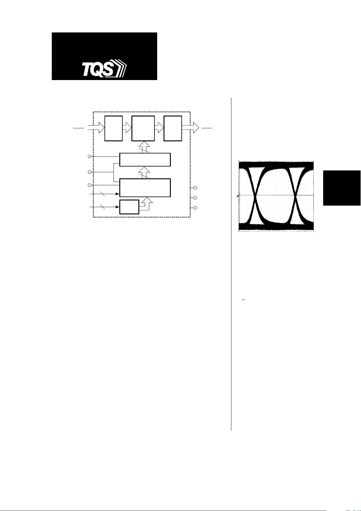
The TQ8016 is a 16 x 16 differential digital crosspoint switch capable of
handling 1.3 Gbit/s data rate. The high data rate and exceptional signal
fidelity is made possible with TriQuint's fully differential Source-Coupled
FET Logic (SCFL) standard cells. The symmetrical switching characteristic
inherent in differential logic results in low signal skew and crosstalk for
maximum signal fidelity.
The user can independently configure any switch output to any input,
including an input chosen by another output. To configure the switch, the
4-bit output address (OA0..3) is decoded to enable the loading of the 4-bit
input selection data (IA0..3) on the rising edge of the LOAD signal. The
process is repeated until all desired connections are programmed. By
bringing the CONFIGURE signal high, the contents of the Output Select
Latches are transferred in parallel to a second row of 4-bit latches (R2),
causing the switch reconfiguration.
This double row architecture minimizes the time to completely reconfigure
the switch since a new set of addresses can be loaded to the Output Select
Latches (R1) while the switch is active (transmitting). At the time of
reconfiguration, no data drop-out occurs for any output whose input
connection does not change.
For applications which do not require synchronous configuration of the
switch, the LOAD and CONFIGURE inputs may be tied together.
Typical output waveform with
all channels driven
Features
• >1.3 Gigabit/sec data rate
• Non-blocking architecture
•
+200 ps delay match (one
input to all outputs)
•
ECL-level data inputs/outputs;
CMOS-level control inputs
• Low crosstalk
• Fully differential data path
• Double row of output select
latches minimizes
reconfiguration time
• Available in 132-pin leaded
chip carrier
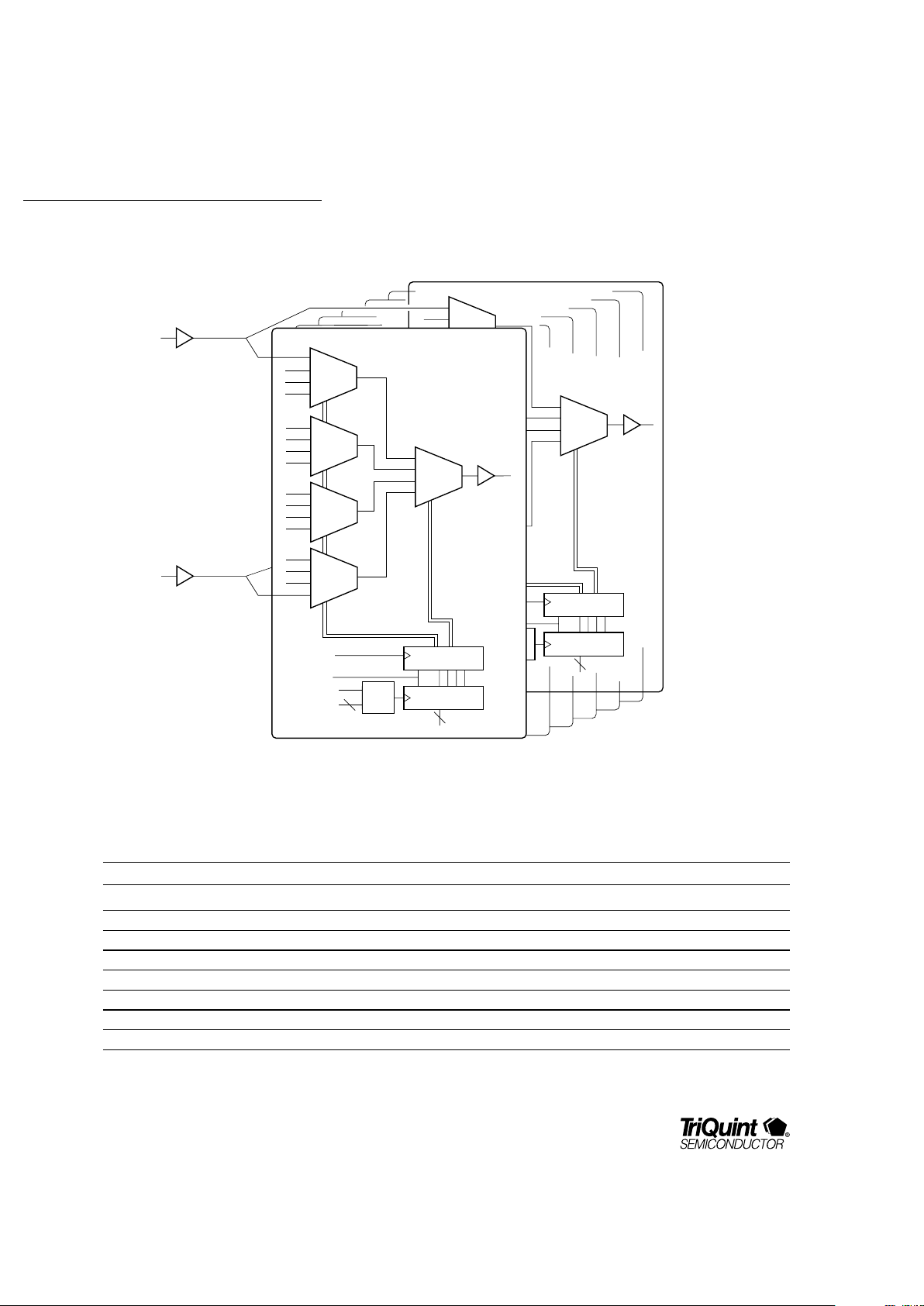
Input
Buffers
Output
Buffers
16 x 16
Crosspoint
Switch
Matrix
64
64
(R2)
Sixteen 4-Bit Latches
(R1)
Sixteen 4-Bit Addressable
Output Select Latches
4
4
4:16
Decoder
VCC
VEE
GND
O0..15
O0..15
D0..15
D0..15
CONFIGURE
RESET
LOAD
IA0..3
OA0..3
TQ8016
TQ8016
For additional information and latest specifications, see our website: www.triquint.com
3
Figure 1. TQ8016 Architecture
Table 1. Pin Descriptions
Pin Name Levels Description
D0–D15 ECL Differential Data Inputs
D0–D15 ECL Differential Data Inputs
D0–D15 ECL Differential Data Inputs
O0–O15 ECL Differential Data Outputs
O0–O15 ECL Differential Data Outputs
IA0–IA3 CMOS Input Address
OA0–OA3 CMOS Output Address
CONFIGURE CMOS Switch Reconfiguration
DATA
OUT 15
(O15)
5
RESET
OUTPUT
SELECT ADDRESS
(OA0:3)
Input
Buffers
DATA
OUT 0
(O0)
Configuration
Register
Program Register
CONFIGURE
LOAD
4
16 X 1-BIT
MULTIPLEXER
16 X 1-BIT
MULTIPLEXER
.
.
.
.
.
.
.
.
.
.
.
.
DATA IN 0
(I0)
DATA IN 15
(I15)
4
INPUT ADDRESS
(IA0:3)
4:16
DECODE
TQ8016
SWITCHING
PRODUCTS
3
For additional information and latest specifications, see our website: www.triquint.com
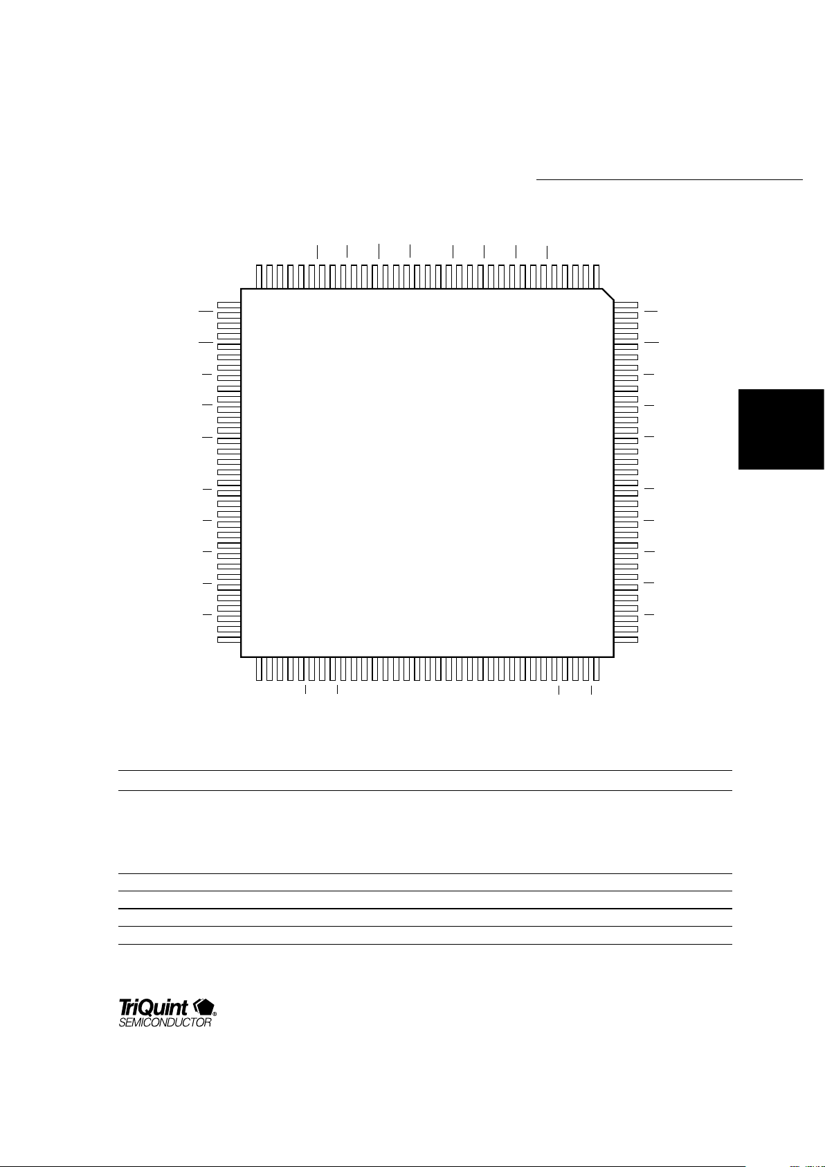
Figure 2. Pinout
VEE
D12
D12
D13
D13
D14
D14
D15
D15
O15
O15
O14
O14
O12
O12
O13
O13
GND
GND
GND
GND
GND
GND
GND
GND
GND
GND
VCC
VCC
O11
O11
O10
O10
O9
O9
O8
O8
O7
O7
GND
GND
GND
GND
O6
O6
O5
O5
O4
O4
O3
O3
O2
O2
GND
GND
VEE
GND
GND
NC
GND
GND
VEE
NCNCGNDO1O1
GNDO0O0
VCC
D1
D1
GND
D0
D0
GND
VCC
D2
D2
GND
D3
D3
GND
D4
D4
GND
D5
D5
GND
D6
D6
GND
NC
GND
D7
D7
GND
D8
D8
GND
D9
D9
GND
D10
D10
GND
D11
D11
VEE
GND
IA3
IA2
GND
IA1
IA0
GNDNCGND
CONFIGURE
LOAD
GND
OA3
OA2
GND
OA1
OA0
NC
NC
NC
NC
RESET
Cavity-Down View
132-Pin Ceramic Chip Carrier
101112131415161718192021222324252627282930313233 123456789
67 68 69 70 71 72 73 74 75 76 77 78 79 80 81 82 83 84 85 86 87 88 89 90 91 92 93 94 95 96 97 98 99
100
101
102
103
104
105
106
107
108
109
110
111
112
113
114
115
116
117
118
119
120
121
122
123
124
125
126
127
128
129
130
131
132
34
35
36
37
38
39
40
41
42
43
44
45
46
47
48
49
50
51
52
53
54
55
56
57
58
59
60
61
62
63
64
65
66
Table 1. Pin Descriptions (continued)
Pin Name Levels Description
RESET CMOS
Configures the switch to
Broadcast
or
Pass-Through
modes, overwriting existing configurations.
Broadcast mode: All output ports are connected to data input port 0.
This mode is selected by applying a RESET “high” pulse with CONFIGURE held “low."
Pass-through mode: I0 is connected to O0, I1 to O1, and so on.
This mode is selected by applying a RESET “high” pulse with CONFIGURE held “high."
LOAD CMOS Loads Input Address
GND 0 V. Ground Reference
VEE –5 V Power Supply
VCC +5 V Power Supply
TQ8016
 Loading...