

TriQuint Semiconductor Inc TQ8015-Q Datasheet
T R I Q U I N T S E M I C O N D U C T O R , I N C .
1
For additional information and latest specifications, see our website: www.triquint.com
SWITCHING
PRODUCTS
Min Max Units
Data Rate/Port 1.25 Gb/s
Jitter 150 ps peak-peak
Channel Propagation Delay 2000 ps
Ch-to-Ch Propagation Delay Skew 500 ps
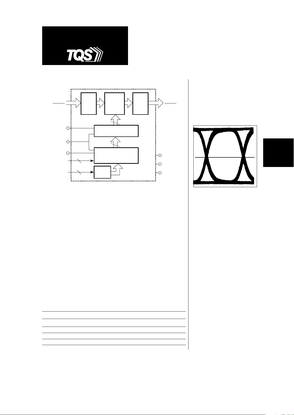
The TQ8015 is a non-blocking 16 x 16 digital crosspoint switch capable of
data rates greater than 1.25 Gigabits per second per port. Utilizing a fully
differential internal data path and ECL I/O, the TQ8015 offers a high data
rate with exceptional signal fidelity. The symmetrical switching and noise
rejection characteristics inherent in differential logic result in low jitter and
signal skew. The TQ8015 is ideally suited for digital video, data
communications and telecommunication switching applications.
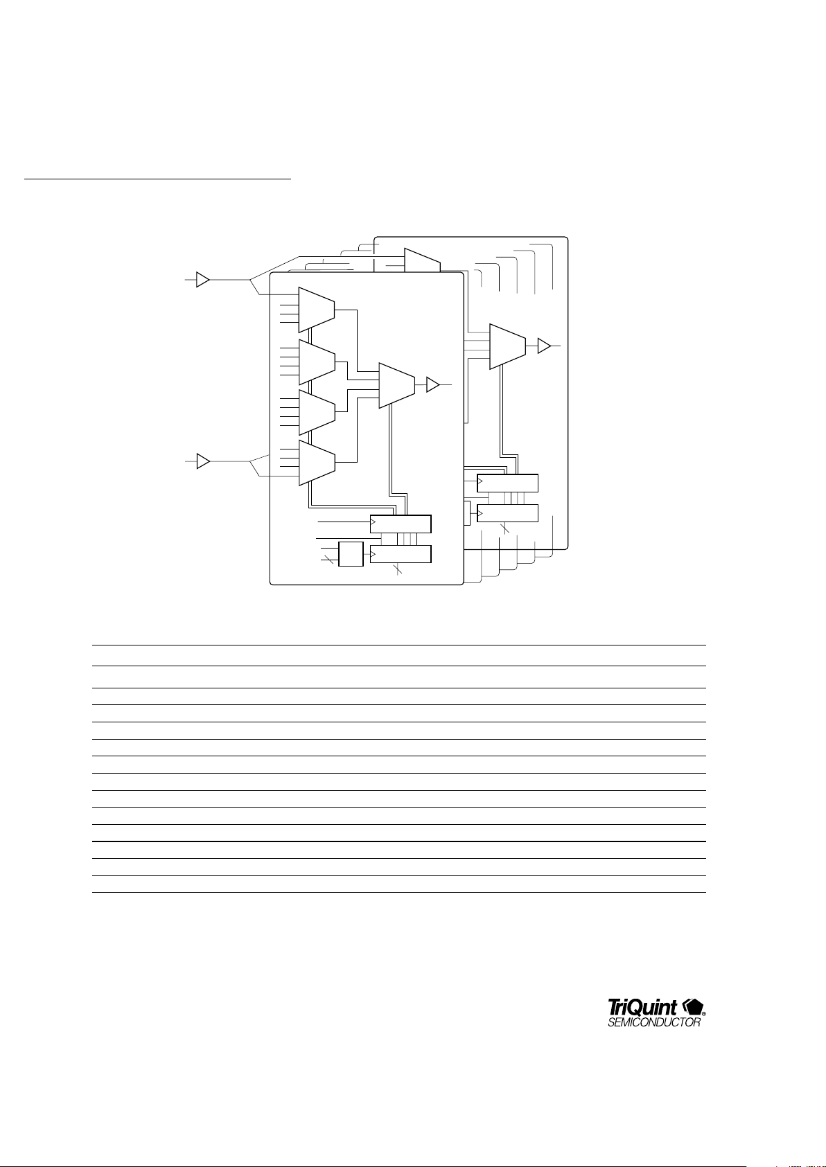
The non-blocking architecture uses 16 fully independent 16:1 multiplexers
(see diagram on page 2), allowing each output port to be independently
programmed to any input port. The switch is configured by sequentially
loading each multiplexer’s 4-bit program latch (OA0:3) with the desired
input port address (IA0:3) and enabling the LOAD pin. When complete, the
CONFIGURE pin is strobed and all new configurations are simultaneously
transferred into the switch multiplexers. Data integrity is maintained on all
unchanged data paths.
Typical output waveform with all
channels driven
Features
• >20 Gb/s aggregate BW
• 1.25 Gb/s/port NRZ data rate
• Non-blocking architecture
• 500 ps delay match
• Differential ECL-level data
I/O; CMOS-level control inputs
• Low jitter and signal skew
• Fully differential data path
• Double buffered configuration
latches
• 132-pin MQFP package
Applications
Telecom/Datacom Switching
Hubs and Routers
Video Switching
TQ8015
1.25 Gigabit/sec
16x16 Digital ECL
Crosspoint Switch
Electrical Characteristics
Input
Buffers
Output
Buffers
16 x 16
Crosspoint
Switch
Matrix
64
64
(R2)
Sixteen 4-Bit Latches
(R1)
Sixteen 4-Bit Addressable
Output Select Latches
4
4
4:16
Decoder
VCC
VEE
GND
O0..15
O0..15
D0..15
D0..15
CONFIGURE
RESET
LOAD
IA0..3
OA0..3
TQ8015
TQ8015
For additional information and latest specifications, see our website: www.triquint.com
2
Figure 1. TQ8015 architecture.
Notes: 1. For die applications.
2. T
C
is measured at case top.
3. All voltages specified with respect to GND, defined as 0V.
4. Subject to I
OUT
and power dissipation limitations.
5. Absolute maximum ratings, as detailed in this table, are the ratings beyond which the device's performance may be impaired
and/or permanent damage to the device may occur.
Symbol Parameter Absolute Max. Rating Notes
T
STOR
Storage Temperature –65° C to +150° C
T
CH
Junction (Channel) Temperature –65° C to +150° C1
T
C
Case Temperature Under Bias –65° C to +125° C2
VCCSupply Voltage 0 V to +7 V 3
V
EE
Supply Voltage –7 V to 0 V 3
V
TT
Load Termination Supply Voltage VEE to 0 V 4
V
IN
Voltage Applied to Any ECL Input; Continuous VEE –0.5 V to +0.5 V
I
IN
Current Into Any ECL Input; Continuous –1.0 mA to +1.0 mA
V
IN
Voltage Applied to Any CMOS Input; Continuous –0.5 V to VCC +0.5 V
I
IN
Current Into Any CMOS Input; Continuous –1.0 mA to +1.0 mA
V
OUT
Voltage Applied to Any ECL Output VEE –0.5 V to +0.5 V 4
I
OUT
Current From Any ECL Output; Continuous –40 mA
P
D
Power Dissipation per Output P
OUT
= (GND – V
OUT
) x I
OUT
50 mW
Table 1. Absolute Maximum Ratings
5
DATA
OUT 15
(O15)
5
RESET
OUTPUT
SELECT ADDRESS
(OA0:3)
Input
Buffers
DATA
OUT 0
(O0)
Configuration
Register
Program Register
CONFIGURE
LOAD
4
16 X 1-BIT
MULTIPLEXER
16 X 1-BIT
MULTIPLEXER
.
.
.
.
.
.
.
.
.
.
.
.
DATA IN 0
(I0)
DATA IN 15
(I15)
4
INPUT ADDRESS
(IA0:3)
4:16
DECODE
TQ8015
SWITCHING
PRODUCTS
3
For additional information and latest specifications, see our website: www.triquint.com
Signal Name/Level Description
I0 to I15, Data input true and complement. Differential data input ports.
NI0 to NI15 Differential ECL
O0 to O15, Data output true and complement. Differential data output ports.
NO0 to NO15 Differential ECL
IA0:3 Input address, CMOS Input port selection address that is written into the selected output port
program latches (OA0:3).
IA3 IA2 IA1 IA0 Input port
0000 0
0001 1
0010 2
:::: :
1111 15
OA0:3 Output select address, CMOS Output port selection address. Selects the output port program latches to
which the input port selection address (IA0:3) is written.
OA3 OA2 OA1 OA0 Output port
0000 0
0001 1
0010 2
:::: :
1111 15
LOAD CMOS Enables the selected output port program latches while set ‘high’.
Latches the data when set to a 'low' level.
CONFIGURE CMOS Transfers the program latches data to the configuration latches and
implements the switch changes while set ‘high’. Latches the data when
set to a ‘low’ level.
RESET CMOS Sets the switch into broadcast or pass-through configuration, overwriting
existing configurations.
Broadcast mode:
All output ports are connected to data input port 0. This
mode is selected by applying a RESET “high” pulse with CONFIGURE held “low”.
Symbol Parameter Min Typ Max Units Notes
T
C
Case Operating Temperature 0 85 °C1
VCCSupply Voltage 4.5 5.5 V
V
EE
Supply Voltage –5.5 –4.5 V
V
TT
Load Termination Supply Voltage –2.0 V 2
R
LOAD
Output Termination Load Resistance 50 Ω 2
Θ
JC
Thermal Resistance Junction to Case 7 °C/W
Table 2. Recommended Operating Conditions
3
Notes: 1. TC measured at case top. Use of adequate heatsink is required.
2. The V
TT
and R
LOAD
combination is subject to maximum output current and power restrictions.
3. Functionality and/or adherence to electrical specifications is not implied when the device is subjected to conditions that exceed,
singularly or in combination, the operating range specified.
Table 3. Pin Descriptions
 Loading...