

TriQuint Semiconductor Inc TQ6124-CM, TQ6124-CD, TQ6124 Datasheet
T R I Q U I N T S E M I C O N D U C T O R , I N C .
1
For additional information and latest specifications, see our website: www.triquint.com
MIXED SIGNAL
PRODUCTS
TQ6124
1 Gigasample/sec,
14-bit
Digital-to-Analog
Convertor
The TQ6124 is a 14-bit monolithic digital-to-analog converter. The TQ6124
achieves conversion accuracy by using a segmented architecture, precision
current sources, and on-chip nichrome resistors. The only external
components required are an external reference and loop control amplifier.
The TQ6124 is ideally suited for applications in direct digital synthesis,
pixel generation for high-resolution monitors, broadband video generation,
and high-speed arbitrary waveform generators.
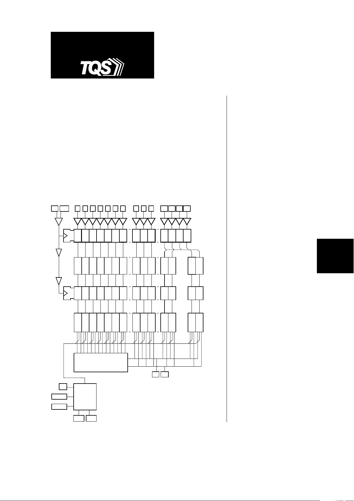
Figure 1. TQ6124 Block Diagram
Features
• 1Gs/s aggregate bandwidth
• 14-bit resolution
• RF front end
• ECL-compatible inputs
• 0.026% DC differential
non-linearity
• 0.035% DC integral non-linearity
• SFDR: 52 dBc @ F
OUT
= 75 MHz
48 dBc @ F
OUT
= 148 MHz
45 dBc @ F
OUT
= 199 MHz
• 1.4 W power dissipation
• 44-pin ceramic QFP package
or die only
Applications
• Direct Digital Synthesis
• Pixel generation for workstations
and high-end monitors
• Direct-generation of broadband
video for cable TV
• High-speed arbitrary waveform
generators
Master
Latch
Segment
Encoders
Delay
Stages
D4 D5 D6 D7 D8 D9 D10 D11 D12 D13
CLK
NCLK
LSBs Intermediate Bits
MSBs
D0 D1 D2 D3
S1 S2
S14 S15
Slave
Latch
...
Current
Switches
Current
Source
Array
V
O
NV
O
V
REF
V
SENSE
50 ohm R-2R Ladder Network
V
AA
MID_trim
LSB_trim
...
...
TQ6124
2
For additional information and latest specifications, see our website: www.triquint.com
Functional Description
The TQ6124 registers incoming bits in a master latch
array. The value of the four most-significant bits is
encoded into an n-of-15 thermometer code while the ten
low-order bits pass though an equalizing delay stage. All
25 bits are re-registered in a 25-wide slave latch array
which drives a set of 25 differential pair switches. These
switches steer the corresponding segment and bit
currents into the true (V
O
) and complementary (NVO)
outputs. This architecture minimizes glitch impulses by
eliminating large mid-scale current transitions.
The most-significant bits generate the segment
currents, which are of equal weight at
1
/16 of the full-
scale output (I
FS
). The ten lower-order bits are divided
into two subgroups. The three intermediate bits steer
binary-weighted currents of magnitude I
FS
/32, IFS/64
and I
FS
/128 to the outputs. The seven least-significant
bits steer identical I
FS
/128 currents into a differential
R-2R ladder to generate effective bit currents of I
FS
/256
to I
FS
/16384. The DAC output is the sum of the
outputs of the segments and the low-order bits.
Clock and data inputs are ECL-compatible. The outputs
are designed to operate into a 50Ω load, with internal
reverse termination to ground being provided by the
R-2R network.
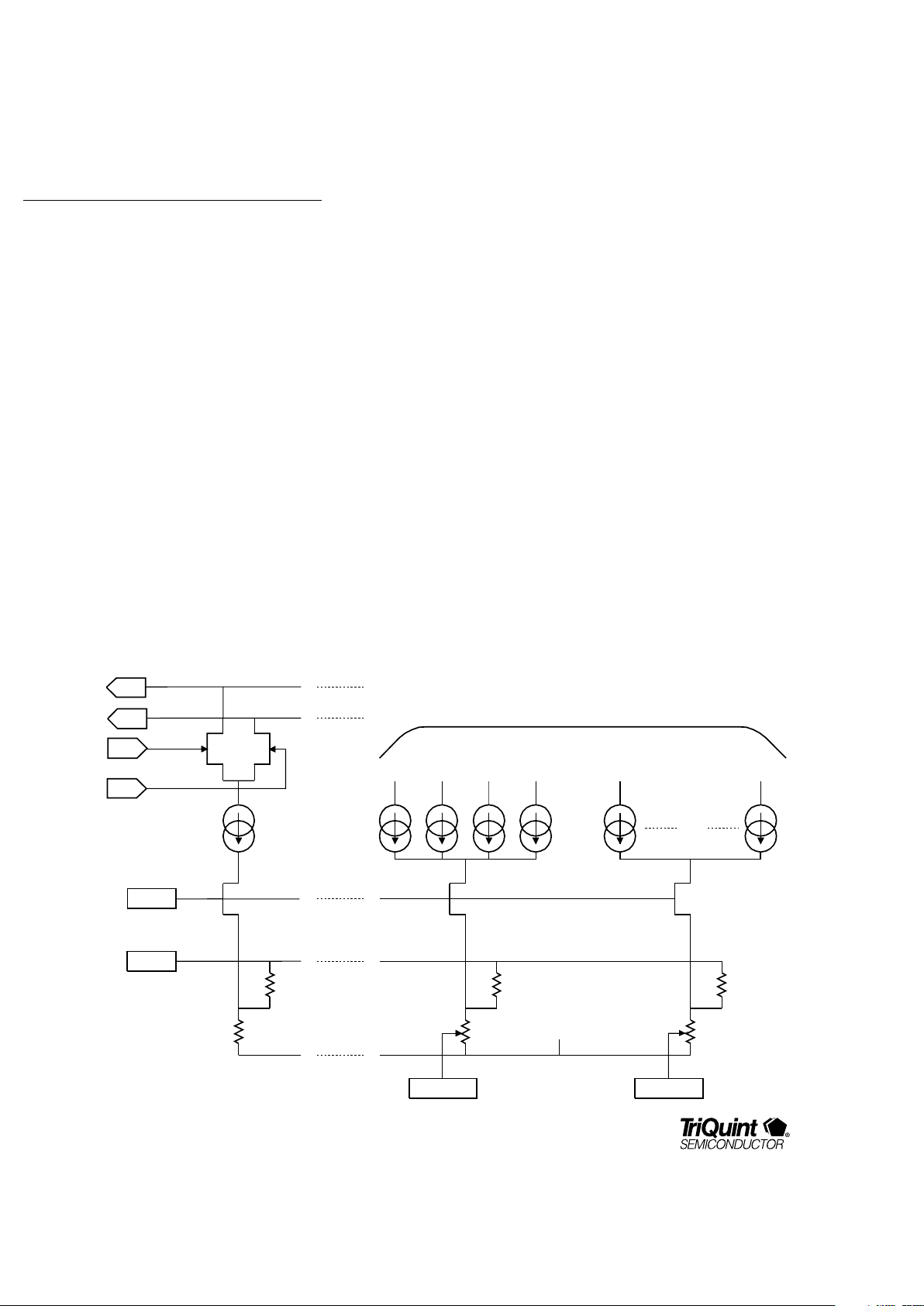
External compensation is utilized to minimize the effects
of device mismatch. An external op amp senses the sum
of the segment, the intermediate bit, and the LSB currents.
Figure 2. TQ6124 Currents
Q
V
O
NQ
NV
O
Segments 1 thru 15
2.5mA
R
SENSE
5.8KΩ
R
SOURCE
1.2KΩ
R
SENSE
5.8KΩ
R
SOURCE
1.2KΩ
1.25mA
.625mA
.3125mA
.3125mA
I
D9
dummy
I
D7
I
D8
R
SENSE
5.8KΩ
R
SOURCE
1.2KΩ
.3125mA
.3125mA
I
D6
dummy
(x8)
To switches for D0 thru D9
MID_trim
LSB_trim
V
AA
V
SENSE
V
REF
TQ6124
3
For additional information and latest specifications, see our website: www.triquint.com
MIXED SIGNAL
PRODUCTS
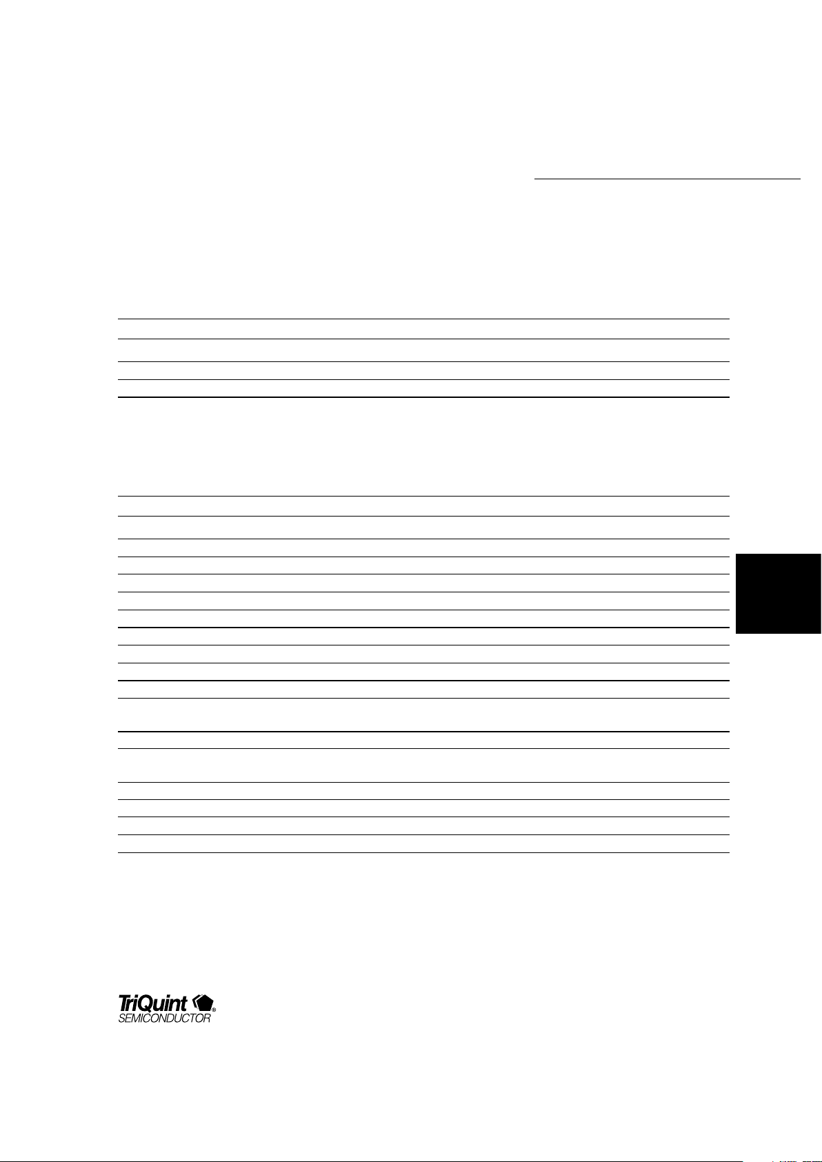
Electrical Specifications
Table 1. Recommended Operating Conditions
Symbol Parameter Min. Nom. Max. Unit
V
SS
Negative Power Supply –5.25 –5.0 –4.75 V
V
AA
Analog Power Supply –15.5 –12 –11.5 V
T
C
Case Temperature –20 85 °C
Table 2. DC Operating Characteristics
Unless otherwise specified, measured over Recommended Operating Conditions with balanced 50Ω loads, V
FS
= 1.0 V.
Symbol Parameter Condition Min. Nom. Max. Unit
I
AA
VAA Supply Current –75 –90 mA
I
SS
VSS Supply Current –285 –450 mA
V
REF
Reference Voltage V
AA
+ 2.5 VAA + 3.0 V
AA
+ 3.75 V
I
REF
Reference input current –25 25 mA
V
IH
ECL Input High Voltage V
EREF
= –1.3 V –1.1 –0.6 V
V
IL
ECL Input Low Voltage V
EREF
= –1.3 V –2.5 –1.5 V
I
I
ECL Input Current –25 25 mA
V
EREF
ECL Reference Voltage V
SS
= –5.0 V –1.34 V
R
EREF
ECL Reference Resistance 400 ohms
DNL Differential non-linearity (Note 2) –0.05 0.026 0.05 %F.S.
INL Integral non-linearity (Note 2) –0.05 0.035 0.05 %F.S.
Full-scale symmetry (Note 1) –8 2 8 mV
V
FS
Full-scale output voltage RL = 50 ohms –1.0 –1.125 V
R
OUT
VO, NVO, output resistance 44 50.9 57 ohms
R
OUT
Matching –2.5 0.15 2.5 %
VO, NV
O
Output Voltage –1.125 0 V
V
ZS
Zero Scale Voltage –50 –40 0 mV
V
SENSE
Sense output voltage V
AA
+ 2.5 V
AA
+ 3.75 V
θ
JC
Thermal Impedance 15 °C/W
Notes: 1. Full-scale symmetry is a measure of the balance between VO and NVO. For a full-scale output transition,
the change in V
O
will match the change in NVO to within the specified amount. Any imbalance in the
output loads will affect symmetry.
2. Linearity can interpreted as 10 bits at
1
/2 LSB or as 11 bits at 1 LSB. The device is monotonic to 10 bits.
Linearity is tested with the Mid_trim set for optimal DNL, with the LSB_trim pin open.
 Loading...