

TriQuint Semiconductor Inc TQ6122-D, TQ6122-M, TQ6122 Datasheet
T R I Q U I N T S E M I C O N D U C T O R , I N C .
1
For additional information and latest specifications, see our website: www.triquint.com
MIXED SIGNAL
PRODUCTS
Features
• 1 Gs/s conversion rate
• 8-bit resolution
• DC differential non-linearity
1
/2 LSB (0.2%)
• DC integral non-linearity
1 LSB (0.4%)
• Settling time 2 ns to 0.4% (est.)
• Spurious-free dynamic range
(SFDR) 45 dBc typical
• ECL-compatible inputs
• Synchronous blanking input
• 1.3 W power dissipation
• 44-pin multilayer ceramic
package or unpackaged die
Applications
• Display generation
• Waveform and signal synthesis
• Video signal reconstruction
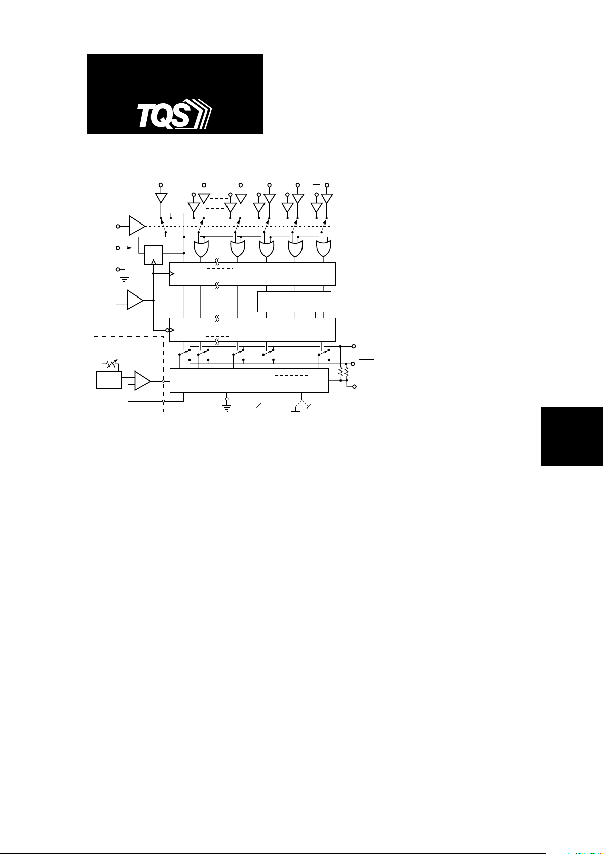
BLANK
A5 A6
B6
A7 (MSB)
B7
MULTIPLEXER
ECL INPUT
BUFFERS
BLANKING
LOGIC
MASTER
LATCH
SLAVE
LATCH
V
(-5 V)
A
BLANK DISABLE
V
V
I
V
BANDGAP
REFERENCE
FULL-SCALE ADJUST
V
CLK
CLK
SELA
BLANK D0 D4
QBLANK Q0 Q4
D5 D6 D7
Q5 Q6 Q7
BINARY-TO-N-OF-7
SEGMENT ENCODER
S1 S2 S3 S4 S5 S6 S7
QS1
QS7
+
–
I
I4
IS1
IS7
+
–
CURRENT-SOURCE ARRAY
50
50
OUT
V
OUT
V
B5B4
BLANK
I0
SENSE
REF
B0
A0
A4
GND
GND
SS
AA
AA
REF
D Q
(-5V)
(EXT. CONTROL LOOP)
D
BLANK D0 D4
QBLANK Q0 Q4
TriQuint's TQ6122 GIGADAC™ is a monolithic, 8-bit digital-to-analog
converter capable of conversion rates to at least 1000 Megasamples/
second. The TQ6122 DAC may be used for display generation, waveform
and signal synthesis, and video signal reconstruction. The TQ6122 features
a 2:1 data MUX at the input for ease of interface and offers synchronous
blanking capability for maximum ease of use in video applications. It drives
complementary 1 V peak-to-peak swings into 50-ohm loads; on-chip 50ohm reverse terminations provide extremely fast settling time.
Due to the inherently high speed of TriQuint's one-micron gate
Enhancement / Depletion-mode gallium arsenide process, the TQ6122
offers guaranteed operation at clock rates of 1000 MHz, with typical room
temperature conversion rates of 1.5 Gs/s without multiplexing and 1.3 Gs/s
when using multiplexed inputs. The TQ6122 features output rise and fall
times of 500 ps (10% – 90%), symmetric complementary output transitions,
and glitch impulse values less than 10 pV/sec. When used for sine wave
synthesis, typical spurious and harmonic free dynamic range is ≥45 dBc.
The TQ6122 may be retrofitted into designs which currently use TriQuint's
TQ6111, 2, 3, 4M DACs with minimal changes to power supply levels and
input and output connections. The part is available in a 44-pin ceramic
package or as unpackaged die.
TQ6122
1 Gigasample/sec,
8-bit Digital-to-Analog
Converter
TQ6122
2
For additional information and latest specifications, see our website: www.triquint.com
Specifications
Table 1. Absolute Maximum Ratings
(1,2)
Symbol Description Min Typ Max Units
A
GND
, D
GND
Analog and digital ground –2 +2 V
V
SS
Digital power –7 V
V
AA
Analog power –10 V
VO, VO (MAX) Analog output (1 V F.S.) –2.5 +2.5 V
VI (MAX) Digital input levels VSS –0.5 +0.5 V
II (MAX) Digital input currents –1 +1 mA
P
D
Power dissipation 3.0 W
T
C
Case backside temperature –65 +135 °C
T
S
Storage temperature –65 +150 °C
Notes: 1. Unless otherwise specified: A
GND
= D
GND
= 0 V, VSS = VAA = –5 V, VFS = 1 V pk–pk, case temperature = 27 °C.
2. Exceeding the absolute maximum ratings may damage the device. The value shown for a particular
parameter is determined with all other parameters at their nominal values.
Table 2. DC Characteristics
(1)
Symbol Description Test Conditions Min. Typ. Max. Unit
V
AA
Analog supply Note 2 –5.25 –4.75 V
I
AA
VAA current VFS = 1 V pk–pk 50 62 80 mA
V
SS
Digital supply Note 2 –5.5 –4.5 V
I
SS
VSS current 145 200 265 mA
P
D
Power dissipation 0.9 1.3 1.85 W
V
ECLREF
ECL reference level Note 3, Figure 1 –1.5 –1.3 –1.1 V
I
ECLREF
ECL ref. input bias current Note 3, Figure 1 ∆V
ECLREF
= ±0.2 V –5 0 +5 mA
R
ECLREF
ECL ref. input resistance Figure 1 50 Ω
C
ECLREF
ECL ref. input capacitance 2 pF
VIH(DC) Data input HIGH (ECL) DC value (V
ECLREF
= –1.3 V) –1100 –500 mV
VIL(DC) Data input LOW (ECL) DC value (V
ECLREF
= –1.3 V) V
TT
–1500 mV
V
CLKH
(DC), Clock HIGH input Differential clock, Note 4 V
ECLREF
+0.3 –0.7 V
V
CLKH
(DC)
V
CLKL
(DC), Clock LOW input Differential clock, Note 4 V
TT
V
ECLREF
–0.3 V
V
CLKL
(DC)
I
IN
Data, clock input bias current VIH = –800 mV, VIL = –1800 mV –25 +25 uA
C
IN
Data, clock input capacitance In multilayer ceramic package 0.5 pF
V
OUT
(MAX), Maximum absolute output level Note 5 +1 V
V
OUT
(MAX)
V
OUT
(MIN), Minimum absolute output level Note 5 –1.5 V
V
OUT
(MIN)
(Continued on next page)
TQ6122
3
For additional information and latest specifications, see our website: www.triquint.com
MIXED SIGNAL
PRODUCTS
V
FS
Full-scale output swing Data bits only, 0–0/1–1 input step 0 1 1.125 V pk–pk
RL = 50 Ω load
V
ZS
Zero-scale offset VFS = 1 V, no external offset, –35 mV
V
BLANK_DISABLE
= 0 V
∆DV
BLANK
Blanking interval Blank input = 1, Notes 6, 7 9 10.4 12 %V
FS
V
BLANK_DISABLE
Blank current disable control Blank current ON –5 (VAA)V
Blank current OFF 0 (A
GND
)V
V
REF
V
REF
input voltage VFS = 1 V peak-to-peak V
AA
+0.7 V
AA
+1.0 V
AA
+1.4 V
VFS = 0 V peak-to-peak V
AA
–1 V
V
SENSE
V
SENSE
output VFS = 1 V peak-to-peak V
AA
+0.8 V
AA
+1.1 V
I
VREF
V
REF
input current V
REF
= V
AA
+0.65 10 uA
V
REF
= V
AA
+1.1 1 mA
I
REF
Ext. reference current output VFS = 1 V peak-to-peak 2 2.5 5 mA
V
IREF
I
REF
terminal voltage –1.5 +1 V
R
OUT, ROUT
V
OUT, VOUT
output resistance 44 50 57 Ω
Matching of R
OUT, ROUT
0.2 2.5 %
C
OUT
V
OUT, VOUT
output capacitance 0.3 pF
Resolution 8 Bits
Monotonicity 8 Bits
DNL Differential non-linearity (± 1/2 LSB) 0.2 % F.S.
INL Integral non-linearity (± 1 LSB) 0.4 % F.S.
Full-scale symmetry VFS = 1 V peak-to-peak, Note 8 –4 +4 mV
VFS temperature coefficient Note 9
Notes: 1. Unless otherwise specified: VAA = –5V ± 5%, VSS = –5 V ±10%, VTT = –2V ± 5%, VFS = 1 V pk–pk, T
CASE
= 0 to +85 °C
2. See the "Power Supplies, Ground and Bypassing" section later in this datasheet for discussion of power supplies.
3. The ECL reference input establishes the switching point for the ECL line receivers used at the DATA, BLANK, and
SELECT inputs. (See Figure 1.) I
ECLREF
is the current required to change the internal ECLREF value by about ±200 mV.
4. Values shown are for differential clock drive, and apply to both CLOCK and CLOCK inputs. For single-ended drive,
the HIGH level should be at least (V
ECLREF
+0.5) volts, but must not exceed –700 mV. The LOW level should be
(V
ECLREF
–0.5) volts, but must not go below VTT, where VTT is the ECL termination voltage (nominal VTT = –2 V).
5. V
OUT
(
MAX
), V
OUT
(
MAX
), V
OUT
(
MIN
), V
OUT
(
MIN
) represent the limits on the absolute output levels, including offset.
6. Blanking interval is the voltage change (as a percentage of the full-scale output swing) added to V
FS
when BLANK is asserted.
7. The BLANK DISABLE input turns OFF the blank current (DV
BLANK
= 0) when held at A
GND
, and turns it ON when pulled to VAA.
8. Full-scale symmetry is a measure of the balance between V
OUT
and V
OUT
. For a full-scale input change (00000000 –> 1111111),
␣␣␣␣the change in V
OUT
will match the change in V
OUT
to within ± 4 mV (1 LSB @ 1 V peak-to-peak).
9. The VFS temperature coefficient is determined primarily by the external reference and loop control op amp.
Table 2. DC Characteristics
(1)
(continued)
Symbol Description Test Conditions Min Typ Max Unit

TQ6122
4
For additional information and latest specifications, see our website: www.triquint.com
Symbol Description Test Conditions Min Typ Max Unit
F
CLK
(MAX) Maximum clock frequency Unmuxed operation 1000 1500 MHz
Muxed operation 1000 1300 MHz
T
RCLK,DATA
Clock, data input rise time 20% to 80% 300 ps
T
FCLK,DATA
Clock, data input fall time 20% to 80% 300 ps
T
WH
Duration of clock HIGH Percentage of clock period 40 50 60 %
T
WL
Duration of clock LOW Percentage of clock period 40 50 60 %
T
SETUP
Data, control setup time See Figure 7 ps
T
HOLD
Data, control hold time See Figure 7 ps
T
ROUT
Output rise time 10% to 90% 300 ps
T
FOUT
Output fall time 10% to 90% 300 ps
T
SETTLE
Output settling time Within ±0.4% of final value 2 ns
Glitch impulse 10 pV/sec
Notes: 1. Unless otherwise specified: VAA = –5V ± 5%, VSS = –5 V + 10% , VFS = 1 V p–p, T
CASE
= 0 to +85 °C,
V
ECL
= –1.3 V, VIH = –0.8 V, VIL = –1.8 V
2. Applies to packaged parts only.
V
IH
V
IL
V
ECL
(-1.3 V NOMINAL)
V
IH
V
IL
(MIN)
(MAX)
V
IH
(MAX)
V
IH
(MIN)
EXTERNAL ECL
REFERENCE
INPUT
I
2 pF
ECL INPUT BUFFERS
R
C
50 Ω
-1.3V
(Nominal,
internal)
ECLREF,
ECLREF
50 Ω
A7, B7
A0, B0
V
SS
ECLREF
–
+
+
–
50 Ω
SELA
BLANK
-5 V
Figure 2. Definition of VIH, VIL for Data and BLANK Inputs
Figure 1. ECL Reference Input Equivalent Circuit
Table 3. AC Characteristics
(1,2)

TQ6122
5
For additional information and latest specifications, see our website: www.triquint.com
MIXED SIGNAL
PRODUCTS
(B) TQ6122 Video DAC Operation (0.679 V Full-Scale)
Blanking current is enabled by connecting BLANK DISABLE to V
AA
.
Input Code V
OUT
(1)
V
OUT
(1)
Full Scale 11111111 –0.679 V –0.071 V
Full Scale – 1 LSB 11111110 –0.676 V –0.074 V
Half Scale + 1 LSB 10000001 –0.343 V –0.407 V
Half Scale 10000000 –0.341 V –0.409 V
Half Scale – 1 LSB 01111111 –0.338 V –0.412 V
Zero Scale + 1 LSB 00000001 –0.003 V –0.747 V
Zero Scale 00000000 ␣ 0.000 V –0.750 V
BLANK = HIGH X . . . . . X –0.750 V ␣ 0.000 V
Input Code V
OUT
(1)
V
OUT
(1)
Full Scale 11111111 –0.996 V ␣ 0.000 V
Full Scale – 1 LSB 11111110 –0.992 V –0.004 V
Half Scale + 1 LSB 10000001 –0.504 V –0.492 V
Half Scale 10000000 –0.500 V –0.496 V
Half Scale –1 LSB 01111111 –0.496 V –0.500 V
Zero Scale + 1 LSB 00000001 –0.004 V –0.992 V
Zero Scale 00000000 ␣ 0.000 V –0.996 V
Figure 3. Typical Digital Input Circuit (Including CLOCK Inputs)
50
50
50
500
500
MICROSTRIP
INPUT
DAC
INPUT PROTECTION
NETWORK
V
TT
–5 V
V
SS
R
IN,
C
IN
TO INPUT
BUFFER
–2 V
(A) TQ6122 Instrumentation DAC operation (1 V Full-Scale)
Blanking current is shunted to ground by tying BLANK DISABLE to A
GND
and forcing BLANK = 0.
Notes: 1. All values shown for V
OUT
and V
OUT
assume identical load resistors (RL1 and RL2 in Figure 5),
and no externally imposed output offset voltage (V
OS
in Figure 5). Zero-scale offset is ignored.
Figure 4. V
OUT
, V
OUT
, and Input Code Relationships for (A) Typical Instrumentation and (B) Video Configurations
TQ6122
6
For additional information and latest specifications, see our website: www.triquint.com
Figure 5. Output Equivalent Circuit, Showing Terminated 50-ohm Transmission Line Loads
Figure 6. Definition of T
WH
and T
WL
T
WL(CLK)
T
WH(CLK)
50%
DIGITAL
INPUT
NON-INVERTING OUTPUT (V )
INVERTING OUTPUT (V )
BOUNDARY
OF DAC
OUT
I
OUT,ROUT
C
50
R
T1
50
R
T2
Z = 50
0
1000 pF
OS (SEE FIG. 18)
(–3V TO +4V)
V
(FOR NO OUTPUT OFFSET)
50
R
L1
50
R
L2
0.1uF
"FAR-END" TERMINATIONS
100 pF
OUT
I
Z = 50
0
OUT
OUT
AGND
TQ6122
7
For additional information and latest specifications, see our website: www.triquint.com
MIXED SIGNAL
PRODUCTS
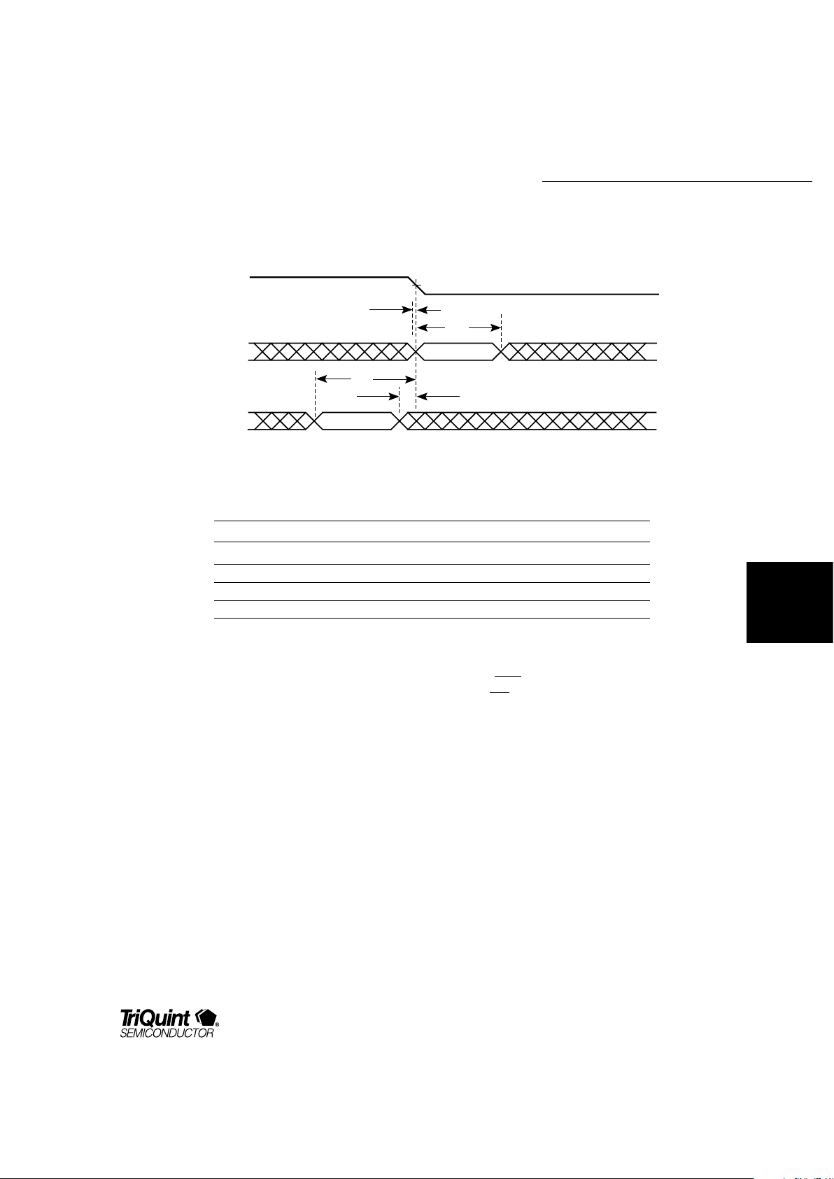
Figure 7. TQ6122 Data and Control Timing
Symbol Description Typical @ 25 °C Unit
T
DS
Data setup time
(1)
0␣ps
TDHData hold time
(2)
+325 ␣ ps
T
SS
SELA setup time
(1,3)
+350 ␣ ps
T
SH
SELA hold time
(2,3)
–100 ␣ ps
Notes: 1. Setup time is defined to be positive for data or control transitions occurring before the negative-going edge of the clock.
2. Hold time is defined to be positive for data or control transitions occurring
after the negative-going edge of the clock.
3. While SELA does not strictly have a setup and hold time, it is convenient to express its allowed transition
region limits in these terms.
SS
T
SELA
DATA
CLOCK
SH
T
DH
T
DS
T
 Loading...