

TriQuint Semiconductor Inc TQ5633 Datasheet
WIRELESS COMMUNICATIONS DIVISION
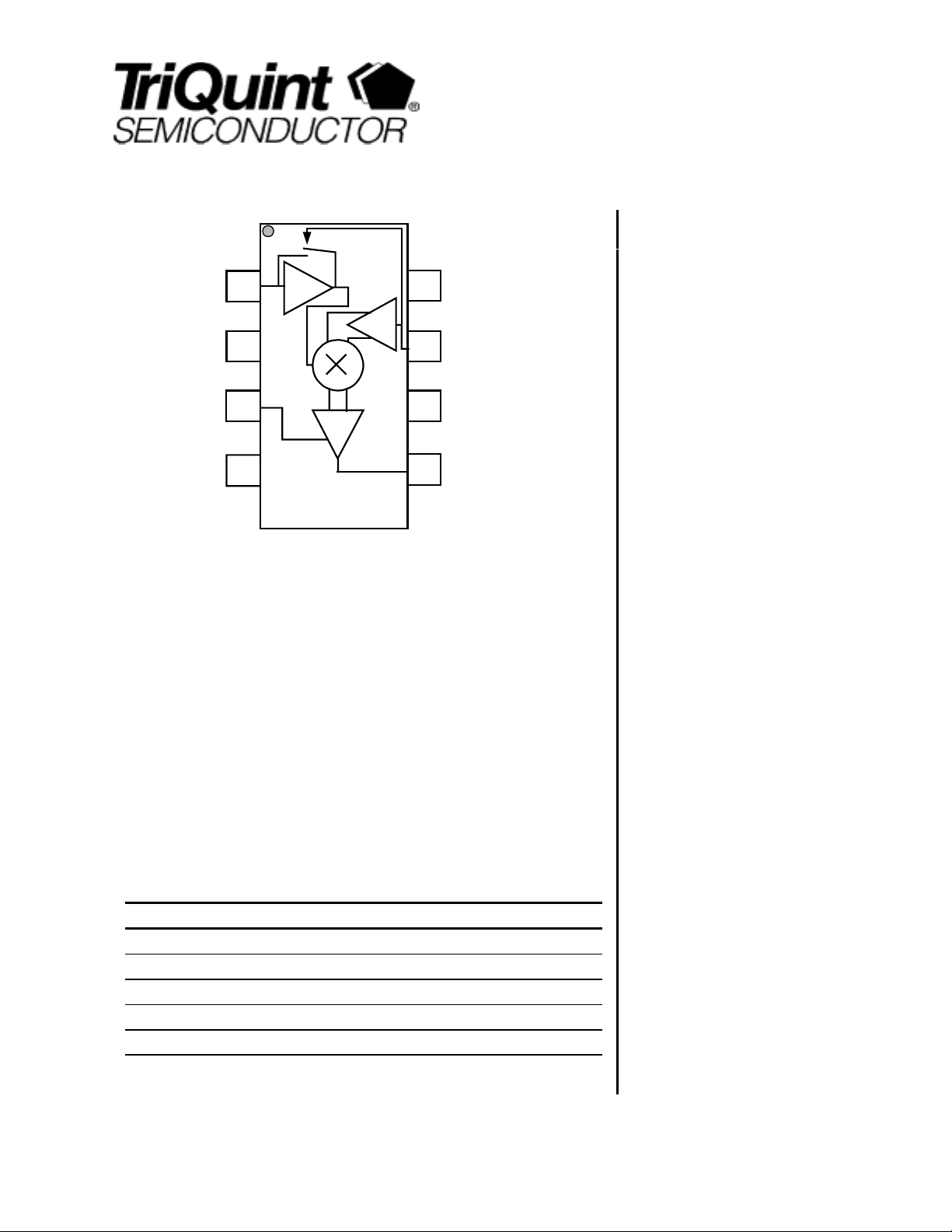
TQ5633
RF
INPUT
IF Common
Mode Tune
Mixer
Vdd
RF
IN
GND
Tune
VDD
VDD
LO
IN
GND
IF
out
RF Amplifier
Vdd
LO Input
RF amplifier
Control
IF
OUTPUT
Product Description
The TQ5633 is a 3V, RF Amplifier/Mixer IC designed specifically for PCS band
CDMA applications. It’s RF performance meets the requirements of products
designed to the IS-95 standard. The TQ5633 is designed to be used with an IF
frequency of 110MHz, and uses a balanced mixer to achieve ½ IF rejection. When
used with the TQ3631 or TQ3632 (CDMA LNAs) it provides a complete CDMA
receiver for 1900MHz phones.
The RF Amplifier/Mixer incorporates on-chip switches which determine two gain
select states. The RF and LO input ports are internally matched to 50
simplifying the design and keeping the number of external components to a
minimum. The TQ5633 achieves good RF performance with low current
consumption, supporting long standby times in portable applications. Coupled with
the very small SOT23-8 package, the part is ideally suited for PCS band mobile
phones.
Electrical Specifications
Parameter Min Typ Max Units
Frequency 1960 MHz
Gain 16.0 dB
Noise Figure 5.8 dB
Input 3rd Order Intercept -0.5 dBm
DC supply Current 23.0 mA
Note 1: Test Conditions: Vdd=2.8V , RF=1960MHz , LO=2070MHz, IF=110MHz, Ta=25C,
1
LO input –4dBm, CDMA High Gain state.
Ω
, greatly
DATA SHEET
3V PCS Band CDMA
RFA/Mixer IC
Features
Small size: SOT23-8
Single 3V operation
Low-current operation
Gain Select
High IP3 performance
Few external components
Excellent ½ IF rejection
110MHz IF Frequency
50 Ω RF and LO inputs
Applications
IS-95 CDMA Mobile Phones
Wireless Local Loop
PCS Micro-cell
For additional information and latest specifications, see our website: www.triquint.com 1
TQ5633
Data Sheet
Electrical Characteristics
Parameter Conditions Min. Typ/Nom Max. Units
RF Frequency PCS band 1930 1960 1990 MHz
IF Frequency 100 110 130 MHz
LO Frequency 2030 2070 2120 MHz
CDMA Mode-High Gain
Gain 14.8 16.0 dB
Noise Figure 5.8 6.7 dB
Input IP3 -1.5 -0.5 dBm
½ IF IIP2 27 dBm
Supply Current 23.0 26.5 mA
CDMA Mode-Low Gain
Gain 5.8 7.0 dB
Noise Figure 10.0 dB
Input IP3 9.5 dBm
½ IF IIP2 32 dBm
Supply Current 18.5 mA
Supply Voltage 2.7 2.8 2.9 V
Note 1: Test Conditions: Vdd=2.8V , RF=1960MHz , LO=2070MHz, IF=110MHz, TC = 25° C, LO input –4dBm, unless otherwise specified.
°
Note 2: Min/Max limits are at +25
C case temperature, unless otherwise specified.
Absolute Maximum Ratings
Parameter Value Units
DC Power Supply 3.6 V
Power Dissipation 500 mW
Operating Temperature -30 to 85 C
Storage Temperature -60 to 150 C
Signal level on inputs/outputs +20 dBm
Voltage to any non supply pin -0.5 to +0.5 V
2 For additional information and latest specifications, see our website: www.triquint.com
TQ5633
Data Sheet
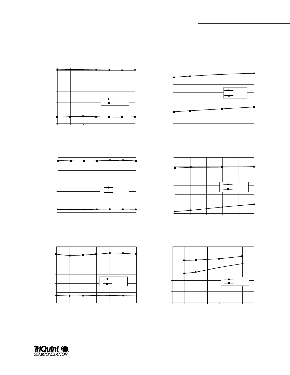
Typical Performance, Note:HG Mode=High Gain Mode, LG Mode=Low Gain Mode
Test Conditions, unless otherwise spec ified: Vdd=2.8V, Ta=25C, RF=1960MHz, LO=2070MHz , IF=110MHz, LO input=-4dBm
Conversion Gain vs Frequency
16
14
12
Gain (dB)
10
8
6
1930 1940 1950 1960 1970 1980 1990
Frequency (MHz)
Input IP3 vs. Frequency
9.5
7.5
5.5
IIP3 (dBm)
3.5
1.5
HG Mode
LG Mode
HG Mode
LG Mode
Conversion Gain vs. Vdd
18
16
14
12
10
Gain (dB)
8
6
4
2.7 2.8 2.9 3 3.1 3.2
Vdd (V)
Input IP3 vs. Vdd
11.5
9.5
7.5
5.5
IIP3 (dBm)
3.5
1.5
HG Mode
LG Mode
HG Mode
LG Mode
-0.5
1930 1940 1950 1960 1970 1980 1990
Frequency (MHz)
Noise Figure vs Frequency
11
10
9
8
7
Noise Figure (dB)
6
5
1930 1940 1950 1960 1970 1980 1990
Frequency (MHz)
HG Mode
LG Mode
-0.5
2.7 2.8 2.9 3 3.1 3.2
Vdd (V)
Half-IF Input IP2 vs. Vdd
40
35
30
25
IIP2 (dBm)
20
15
2.6 2.7 2.8 2.9 3 3.1 3.2 3.3
Vdd (V)
HG Mode
LG Mode
For additional information and latest specifications, see our website: www.triquint.com 3
 Loading...