

TriQuint Semiconductor Inc TQ5132 Datasheet
WIRELESS COMMUNICATIONS DIVISION
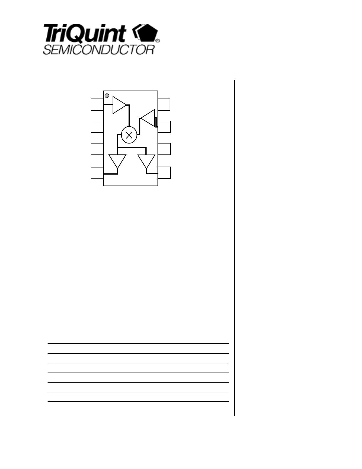
Control 2
RFA Gain
Select
RF
IN
GND
GIC
VDD
LO
IN
Mode Select/
Control 3
IFA Gain
TQ5132
DATA SHEET
Control 1
3V Cellular Band
LO Input
CDMA/AMPS RFA/Mixer
IC
Select
CDMA
IF Out
IF
Out
IF
Out
AMPS
IF Out
Product Description
The TQ5132 is a 3V, RFA/Mixer IC designed specifically for Cellular band
CDMA/AMPS applications. It’s RF performance meets the requirements of products
designed to the IS-95 and AMPS standards. The TQ5132 is designed to be used
with the TQ3131 or TQ3132 (CDMA/AMPS LNA) which provides a complete CDMA
receiver for 800MHz dual-mode phones.
The RFA/Mixer incorporates on-chip switches which determine CDMA, AMPS and
bypass mode select. When used with the TQ3131 or TQ3132 (CDMA/AMPS LNA),
four gain steps are available. The RF input port is internally matched to 50 Ω,
greatly simplifying the design and keeping the number of external components to a
minimum. The TQ5132 achieves good RF performance with low current
consumption, supporting long standby times in portable applications. Coupled with
the very small SOT23-8 package, the part is ideally suited for Cellular band mobile
phones.
Electrical Specifications
Parameter Min Typ Max Units
Frequency 881 MHz
Gain 15.0 dB
Noise Figure 4.5 dB
Input 3rd Order Intercept 2.5 dBm
DC supply Current 15.0 mA
Note 1: Test Conditions: Vdd=2.8V, RF=881MHz, LO=966MHz, IF=85MHz, Ta=25C, CDMA High Gain
state.
1
Features
Small size: SOT23-8
Single 3V operation
Low-current operation
Gain Select
Mode Select
High IP3 performance
Few external components
Applications
IS-95 CDMA Mobile Phones
AMPS Mobile Phones
Dual Mode CDMA Cellular application
For additional information and latest specifications, see our website: www.triquint.com 1
TQ5132
Data Sheet
Electrical Characteristics
Parameter Conditions Min. Typ/Nom Max. Units
RF Frequency Cellular band 869 881 894 MHz
IF Frequency Range High side LO 85 130 MHz
CDMA Mode-Hi gh Gain
Gain 12.6 16.0 18.2 dB
Noise Figure 4.5 7.2 dB
Input IP3 -2.2 2.5 dBm
Supply Current (TA = 25°C)
CDMA Mode-Hi gh Gain Low Linearity
Gain 18.5 dB
Noise Figure 4.0 dB
Input IP3 -0.3 dBm
Supply Current (TA = 25°C)
CDMA Mode-Mid Gain
Gain 5.0 dB
Noise Figure 11.0 dB
Input IP3 14.0 dBm
Supply Current (TA = 25°C)
CDMA Mode-Low Gain
Gain 5.2 8.0 10.2 dB
Noise Figure 10.0 12.8 dB
Input IP3 7.4 11.0 dBm
Supply Current (TA = 25°C)
AMPS Mode
Gain 7.7 12.0 12.6 dB
Noise Figure 5.0 7.7 dB
Input IP3 -4.9 -1.0 dBm
Supply Current (TA = 25°C)
Supply Voltage 2.8 3.15 V
Note 1: Test Conditions: Vdd=2.8 to 3.15V, RF=869-894MHz, LO= High side –6 to –2dBm, IF=8 5MHz, TA= -30 to 85° C, unless otherwise sp ecified.
Absolute Maximum Ratings
Parameter Value Units
DC Power Supply 5.0 V
Power Dissipation 500 mW
Operating Temperature -30 to 85 C
Storage Temperature -60 to 150 C
Signal level on inputs/outputs +20 dBm
Voltage to any non supply pin +0.3 V
18.0 21.0 mA
18.0 mA
13.5 mA
14.0 17.5 mA
9.0 10.3 mA
2 For additional information and latest specifications, see our website: www.triquint.com
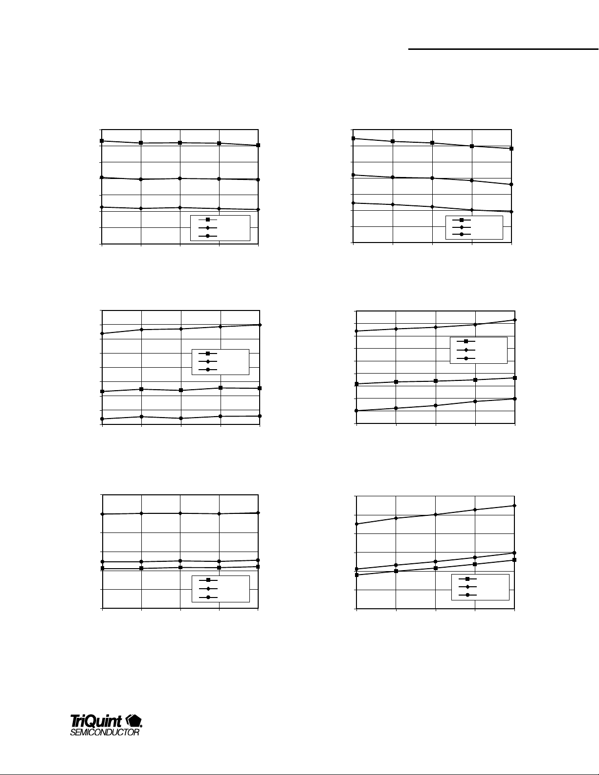
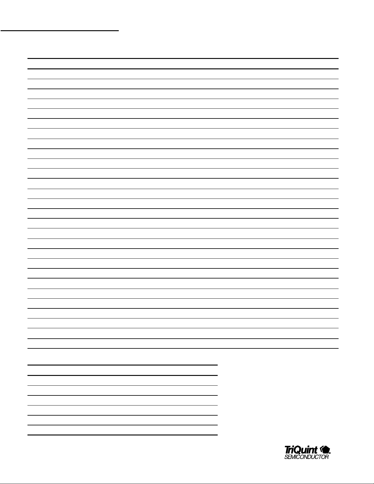
Typical Performance, Note: HG Mode=CDMA High Gain, LG Mode=CDMA Low Gain
Test Conditions, unless otherwise specified: Vdd=2.8V, Ta=25C , RF=881MHz, LO=966MHz , LO input=-4dBm, IF=85MHz
Gain vs. Frequency
18
16
14
12
10
Gain (dB)
8
6
4
869 875 882 888 894
Frequency (MHz)
HG Mode
LG Mode
AMPS
18
16
14
12
10
Gain (dB)
8
6
4
-30 0 25 55 85
Gain vs. Temperature
Temperature (Celsius)
TQ5132
Data Sheet
HG Mode
LG Mode
AMPS
Input IP3 vs. Frequency
14
12
10
8
6
4
Input IP3 (dBm)
2
0
-2
869 875 882 888 894
Frequency (MHz)
Noise Figure vs. Frequency
12
10
8
6
4
Noise Figure (dB)
2
0
869 875 882 888 894
Frequency (MHz)
HG Mode
LG Mode
AMPS
HG Mode
LG Mode
AMPS
Input IP3 vs. Temperature
14
12
10
8
6
4
2
Input IP3 (dBm)
0
-2
-4
-30 0 25 55 85
Temperature (Celsius)
Noise Figure vs. Temperature
HG Mode
LG Mode
AMPS
12
10
8
6
4
Noise Figure (dB)
2
HG Mode
LG Mode
AMPS
0
-30 0 25 55 85
Temperature (Celsius)
For additional information and latest specifications, see our website: www.triquint.com 3
TQ5132
Data Sheet
Idd vs. Temperature
20
18
16
14
12
10
Idd (mA)
8
6
4
2
HG Mode
LG Mode
AMPS
0
-30 0 25 55 85
Temperature (Celsius)
Gain vs. LO Power
18
16
14
12
10
8
Gain (dB)
6
4
2
HG Mode
LG Mode
AMPS
0
-6 -4 -2
LO Power (dBm)
Noise Figure vs. LO Power
12
10
8
6
4
Noise Figure (dB)
2
HG Mode
LG Mode
AMPS
0
-6 -4 -2
LO Power (dBm)
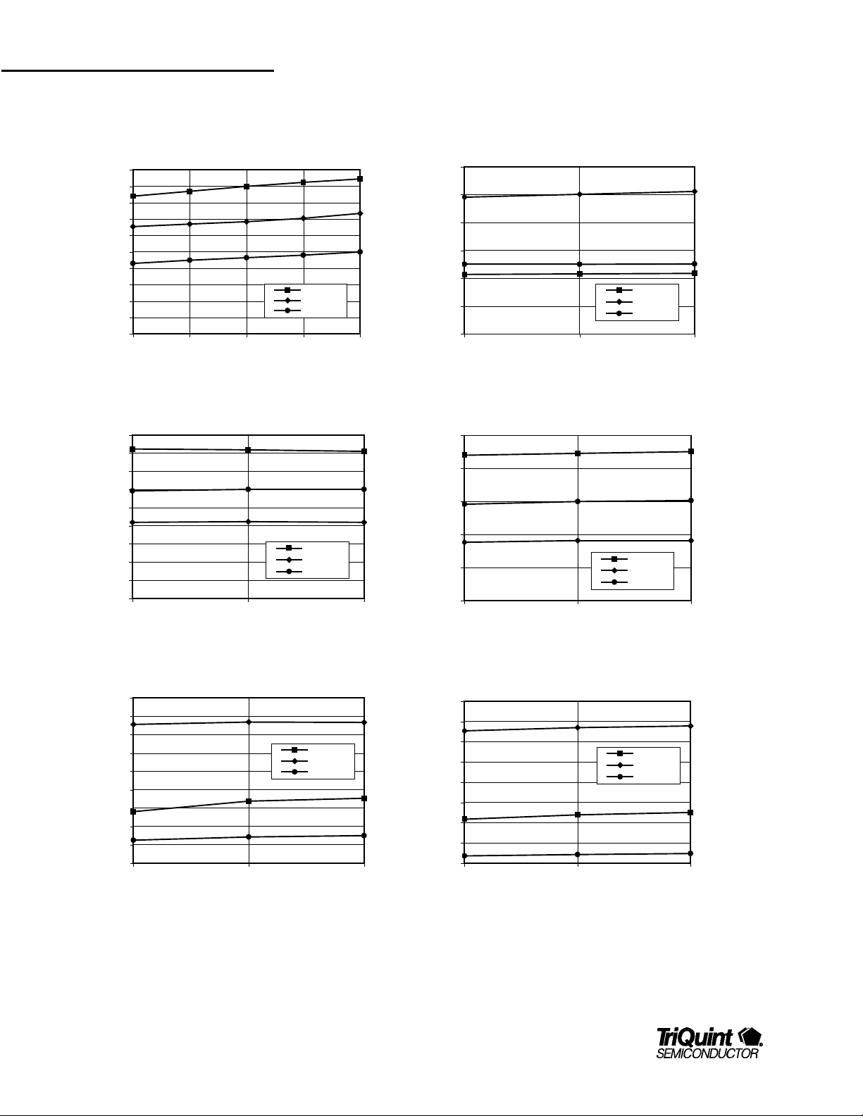
Gain vs. Vdd
18
15
12
Gain (dB)
9
6
HG Mode
LG Mode
AMPS
3
2.8 3 3.15
Vdd (volts)
Input IP3 vs. LO Power
14
12
10
8
6
HG Mode
LG Mode
AMPS
4
2
Input IP3 (dBm)
0
-2
-4
-6 -4 -2
14
12
10
8
6
4
Input IP3 (dBm)
2
0
-2
2.8 3 3.15
LO Power (dBm)
4 For additional information and latest specifications, see our website: www.triquint.com
Input IP3 vs. Vdd
HG Mode
LG Mode
AMPS
Vdd (volts)
 Loading...