

TriQuint Semiconductor Inc TQ5122 Datasheet
WIRELESS COMMUNICATIONS DIVISION
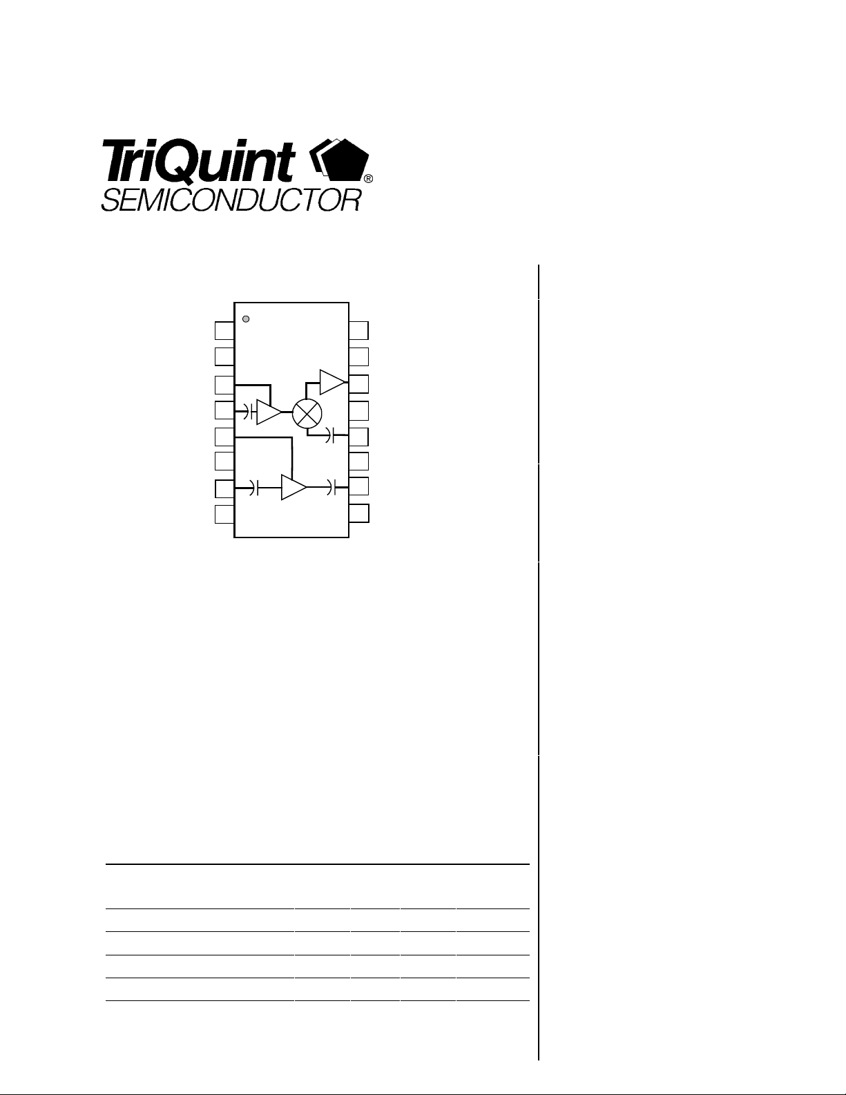
GND
1
GND
16
TQ5122
DATA SHEET
GND
Vdd MXR
MXR LO
VDD LNA
GND
RF IN
GND
2
3
4
5
6
7
8
15
GND
14
IF Output/Vdd
13
GND
MXR RF
12
GND
11
LNA
10
Out
9
Control
Input
Sleep
Product Description
The TQ5122 is a 3V, RF receiver IC designed specifically for Cellular band TDMA
applications. It’s RF performance meets the requirements for products designed to the
IS-136 TDMA and the AMPS standards. The TQ5122 includes a power–down mode
which allows current saving during standby and the non-operating portion of the TDMA
pulse. The TQ5122 contains LNA and Mixer circuits matched to the 800MHz cellular
band.
The mixer uses a high-side LO frequency. The IF has a usable frequency range of 85
to 150MHz. The LNA Output and Mixer Input ports are internally matched to simplify
the design and keep the number of external components to a minimum. The TQ5122
achieves excellent RF performance with low current consumption which yields long
standby times in portable applications. The small QSOP-16 package is ideally suited
for Cellular band mobile phones.
Electrical Specifications
1
3V Cellular TDMA/AMPS
Receiver IC With PowerDown
Features
Power-Down, “Sleep” Mode
Single 2.8V operation
Low-current operation
Small QSOP-16 plastic package
Few external components
Applications
IS-136 TDMA Mobile Phones
Dual Mode TDMA/AMPS Mobile Phones
AMPS Mobile Phones
Parameter Min Typ Max Units
Frequency 869 894 MHz
Gain 18.5 dB
Noise Figure 2.7 dB
Input 3rd Order Intercept -8.5 dBm
DC supply Current 12.0 mA
Note 1: Test Conditions: Vdd= 2.8VDC, Tc=25°C, Filter IL=2.5dB, RF=881MHz, LO=1016MHz,
IF=135MHz, LO input=-7dBm
For additional information and latest specifications, see our website: www.triquint.com 1
TQ5122
Data Sheet
Electrical Characteristics
Parameter Conditions Min. Typ/Nom Max. Units
RF Frequency 869 894 MHz
LO Frequency 954 1044 MHz
IF Frequency 85 150 MHz
LO input level -7 -4 0 dBm
Supply voltage 2.7 2.8 4.0 V
Gain 16.0 18.5 dB
Gain Variation vs. Temp. -40 to 85 °C +/-2.0 dB
Noise Figure 2.7 3.5 dB
Input 3rd Order Intercept -11.0 -8.5 dBm
Return Loss LNA input – with external match
Isolation LO to LNA RF in
IF Output Impedance Vdd = 2.8V; Sleep mode, Device On
Power Down, “sleep” Device On Voltage
Supply Current, Sleep mode, Device On Tc = + 25 °C 12 15 mA
Supply Current, Sleep mode, Device Off Enable voltage = 0, LO Drive off 100 1000
1,2
dB
dB
dB
dB
dB
dB
dB
Ohm
Ohm
Ohm
VDC
µA
LNA output
Mixer RF input
Mixer LO input
LO to IF; after IF match
RF to IF; after IF match
Vdd = 2.8V; Sleep mode, Device Off
Vdd = 0V
Device Off Voltage 0
10
10
10
10
35
40
20
500
Approx. Open
<50
Vdd
0
Vdd VDC
Operating Temperature, case -40 25 +85 °C
Note 1: Test Conditions: Vdd=2.8VDC, Fil ter IL=2.5dB, RF=881MHz, LO=1016MHz, IF=135MHz, LO input=-7dBm, TC = 25°C, unless otherwise specified.
Note 2: Min./Max. limi ts are at +25
°
C case temperature unless otherwise spec ified.
Absolute Maximum Ratings
Parameter Value Units
DC Power Supply 5.0 V
Power Dissipation 500 mW
Operating Temperature -55 to 100 °C
Storage Temperature -60 to 150 °C
Signal level on inputs/outputs +20 dBm
Voltage to any non supply pin -0.3 to Vdd + 0.3 V
2 For additional information and latest specifications, see our website: www.triquint.com
TQ5122
Data Sheet
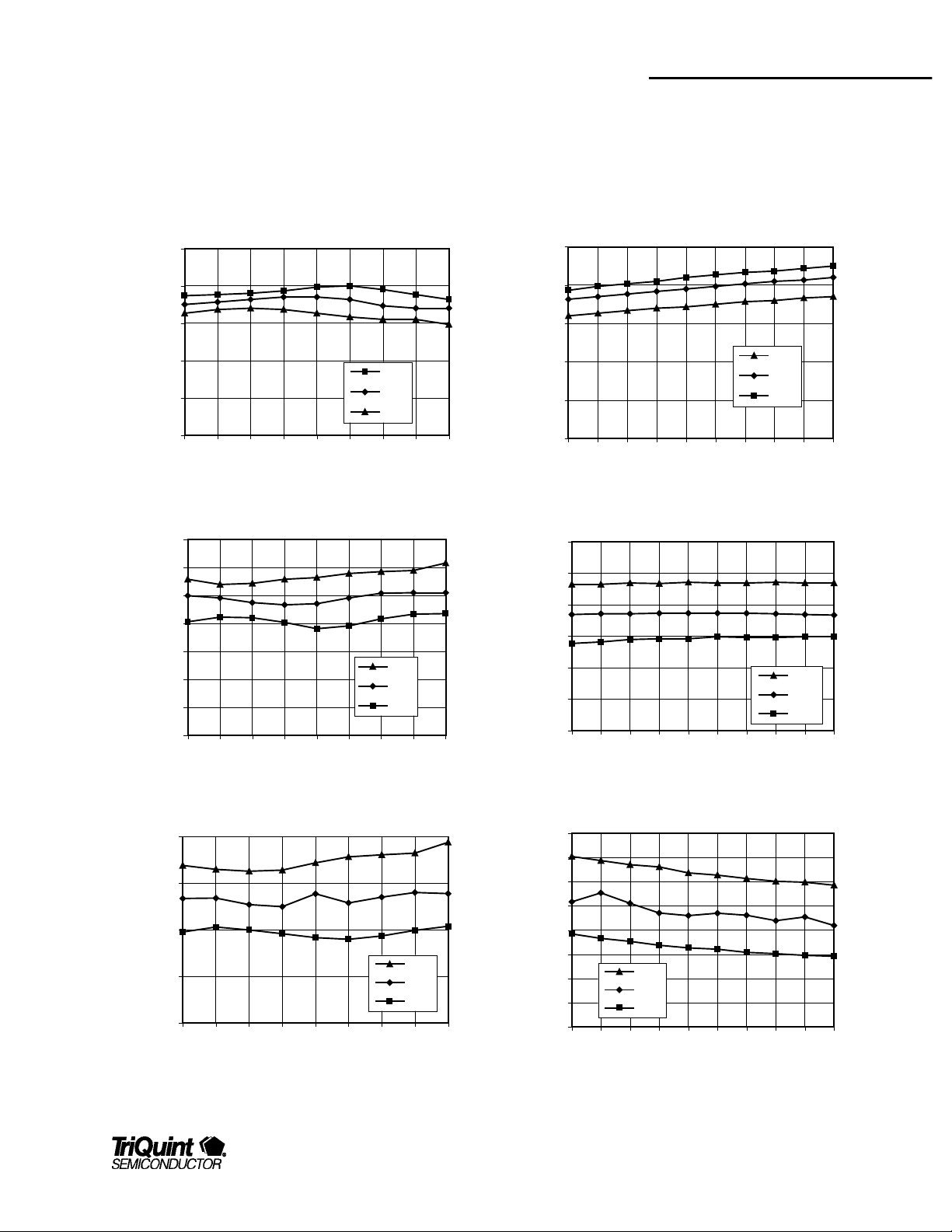
Typical Performance
Test Conditions (Unl ess Otherwise Speci fied): Vdd=2.8VDC, Tc=25°C, filter IL=2.5dB, RF=881MHz, LO=1016MHz, IF= 135MHz, LO input=-7dBm
Gain vs. Frequency vs. Temperature
25
20
15
Gain (dB)
10
5
0
869 872 875 878 881 884 887 890 893
Frequency (MHz)
Input IP3 vs. Frequency vs. Temperature
-40C
+25C
+85C
-4
-6
-8
-10
-12
Input IP3 (dBm)
-14
-16
85C
25C
-40C
-18
869 872 875 878 881 884 887 890 893
Frequency (MHz)
25
20
15
Gain (dB)
10
5
0
2.7 2.8 2.9 3 3.1 3.2 3.3 3.4 3.5 3.6
-4
-6
-8
-10
-12
Input IP3 (dBm)
-14
-16
2.7 2.8 2.9 3 3.1 3.2 3.3 3.4 3.5 3.6
Gain vs. Vdd vs. Temperature
+85C
+25C
-40C
Vdd (volts)
Input IP3 vs. Vdd vs. Temperature
Vdd (volts)
+85C
+25C
-40C
NF vs. Frequency vs. Temperature
4
3
2
NF (dB)
1
0
869 872 875 878 881 884 887 890 893
Frequency (MHz)
+85C
+25C
-40C
For additional information and latest specifications, see our website: www.triquint.com 3
4
3.5
3
2.5
2
NF (dB)
1.5
1
0.5
0
2.7 2.8 2.9 3 3.1 3.2 3.3 3.4 3.5 3.6
NF vs. Vdd vs. Temperature
+85C
+25C
-40C
Vdd (volts)
 Loading...