

TriQuint Semiconductor Inc TQ5121 Datasheet
WIRELESS COMMUNICATIONS DIVISION
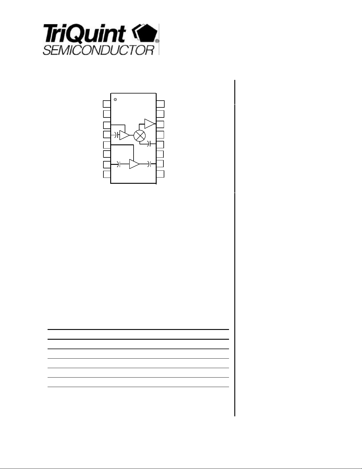
TQ5121
Optional
N/C
N/C
Vdd MXR
MXR LO
VDD LNA
GND
RF IN
GND
1
2
3
4
5
6
7
8
16
15
14
13
12
11
10
9
GND
N/C
Mixer IF/
Vdd
GND
MXR RF
GND
LNA
Out
N/C
Product Description
The TQ5121 is a 3V, RF receiver IC designed specifically for Cellular band TDMA
applications. It’s RF performance meets the requirements of products designed to
the IS-136 and AMPS standards. The TQ5121 is pin compatible with TQ9222, which
enables handset designers to use strategic board platform strategy. The TQ5121
contains LNA+Mixer circuits to handle the 800MHz cellular band.
DATA SHEET
3V Cellular TDMA/AMPS
LNA/mixer Receiver IC
Features
§ Pin compatible with TQ9222
(dual-band TDMA receiver)
§ Single 3V operation
§ Low-current operation
§ 50 Ω matched inputs
§ QSOP-16 plastic package
The mixer uses a high-side LO frequency, with the IF covering a range of 70 to
140MHz. Most RF ports are internally matched to 50 Ω, greatly simplifying the
design and keeping the number of external components to a minimum. The TQ5121
achieves good RF performance with low current consumption, supporting long
standby times in portable applications. Coupled with the very small QSOP-16
package, the part is ideally suited for Cellular band mobile phones.
Applications
§ IS-136 Mobile Phones
§ AMPS Mobile Phones
Electrical Specifications
Parameter Min Typ Max Units
Frequency 869 894 MHz
Gain 17.5 dB
Noise Figure 2.7 dB
Input 3rd Order Intercept -8.5 dBm
DC supply Current 10.0 mA
Note 1: Test Conditions: Vdd=2.8V, Ta=25C, filter IL=2.5dB, RF=881MHz, LO=991MHz, IF=110MHz,
LO input=-7dBm
For additional information and latest specifications, see our website: www.triquint.com 1
1
§ ISM 900MHz
TQ5121
Data Sheet
Electrical Characteristics
Parameter Conditions Min. Typ/Nom Max. Units
RF Frequency Cellular band 869 894 MHz
LO Frequency Cellular band 950 1040 MHz
IF Frequency Cellular band 70 140 MHz
LO input level -7 -4 0 dBm
Supply voltage 2.7 2.8 4.0 V
Gain 16.0 17.5 dB
Gain Variation vs. Temp. -40 to 85C -2.0 +2.0 dB
Noise Figure 2.7 3.5 dB
Input 3rd Order Intercept -11.0 -8.5 dBm
Return Loss LNA input – external match
LNA output
Mixer RF input
Mixer LO input
Isolation LO to LNA in
LO to IF; after IF match
RF to IF; after IF match
IF Output Impedance Vdd = 2.8V; “ON”
Vdd = 0V; “OFF”
Supply Current 10 13 mA
Temperature -40 25 85 C
Note 1: Test Conditions: Vdd=2.8V, filter IL=2.5dB, RF=881MHz, LO=991MHz, IF=110MHz, LO input=-7dBm, TC = 25° C, unless otherwise specified.
10
10
10
10
40
40
40
500
<50
dB
dB
dB
dB
dB
dB
dB
Ohm
Ohm
Absolute Maximum Ratings
Parameter Value Units
DC Power Supply 5.0 V
Power Dissipation 500 mW
Operating Temperature -55 to 100 C
Storage Temperature -60 to 150 C
Signal level on inputs/outputs +20 dBm
Voltage to any non supply pin +.3 V
2 For additional information and latest specifications, see our website: www.triquint.com
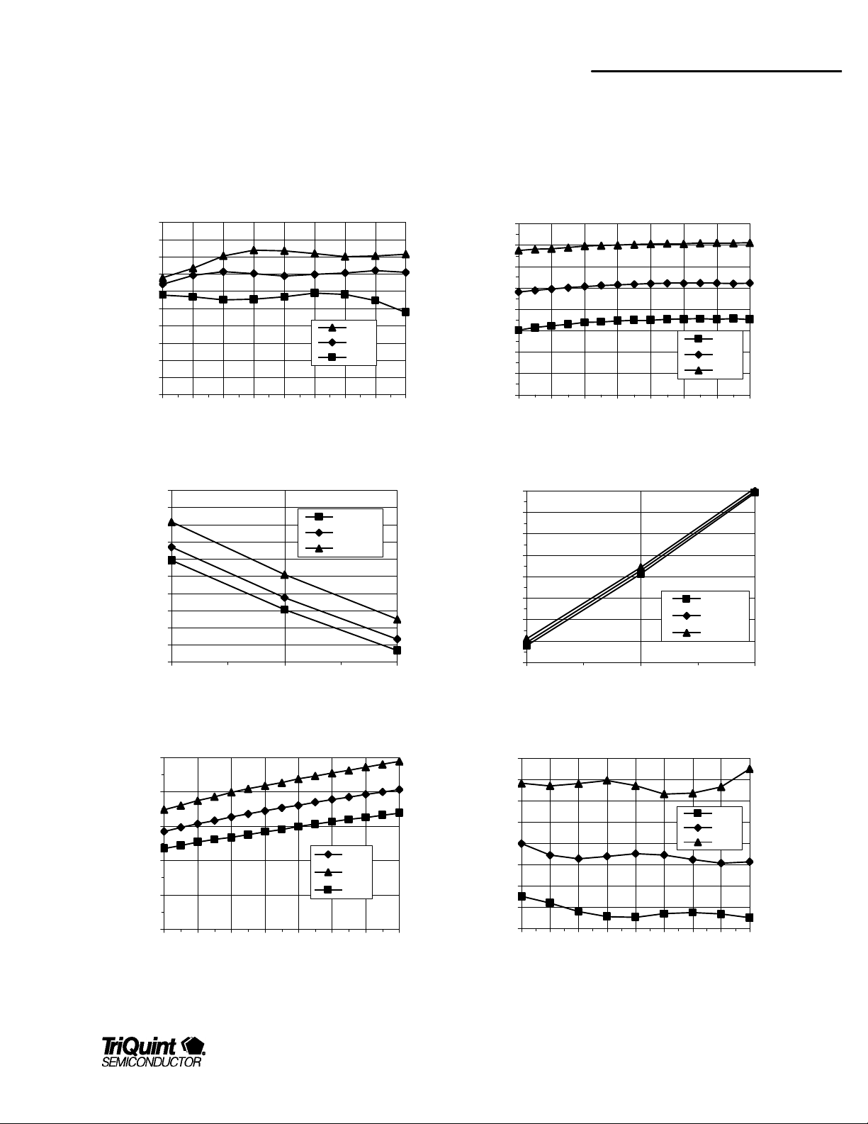
TQ5121
CG vs. Freq vs. Temp
CG vs. Temp vs. Vdd
CG vs. Vdd vs. Temp
Data Sheet
Typical Performance
Test Conditions (Unless Otherwise Specified): Vdd=2.8V, Ta=25C, filter IL=2.5dB, RF=881MHz, LO=991MHz, IF=110MHz, LO input=-7dBm
IIP3 vs. Vdd vs. Temp
20
19
18
17
16
15
Gain (dB)
14
13
12
11
10
869 872 875 878 881 884 887 890 893
20
19.5
19
18.5
18
17.5
Gain (dB)
17
16.5
16
15.5
15
-40 25 85
Freq (MHz)
Temp C
-40C
+25C
+85C
Vdd=2.7v
Vdd=2.8v
Vdd=3.0v
-6
-7
-8
-9
-10
IIP3 (dBm)
-11
-12
-13
-14
2.5 2.6 2.7 2.8 2.9 3 3.1 3.2
Vdd (volts)
IIP3 vs. Temp vs. Vdd
-7
-7.5
-8
-8.5
-9
IIP3 (dBm)
-9.5
-10
-10.5
-11
-40 25 85
Temp C
-40C
+25C
+85C
Vdd=2.7
Vdd=2.8
Vdd=3.0
20
18
16
Gain (dB)
14
12
10
2.5 2.6 2.7 2.8 2.9 3 3.1 3.2
Vdd (volts)
+25C
-40C
+85C
For additional information and latest specifications, see our website: www.triquint.com 3
Noise Figure vs. Freq vs. Temp
4
3.75
3.5
3.25
3
NF
2.75
2.5
2.25
2
869 872 875 878 881 884 887 890 893
Freq (MHz)
-40C
+25C
+85C
 Loading...